

Page 1
19-0144; Rev. 0; 9/93
Complete 230kbps, 2.7V to 5.25V
Serial Interface for Notebook Computers
_______________General Description
The MAX562 is designed specifically for notebook and
palmtop computers that need to transfer data quickly.
It runs at data rates up to 230kbps, and has a guaranteed 4V/µs slew rate. This device meets the new
EIA/TIA-562 standard that guarantees compatibility with
RS-232 interfaces.
The MAX562 has low-power shutdown and keep-awake
modes. In keep-awake mode, the transmitters are disabled but all receivers are active, allowing unidirectional communication. In shutdown mode, the entire chip is
disabled and all outputs are in a high-impedance state.
The MAX562 is available in a standard 28-pin SO package, and in a smaller footprint shrink small-outline
package (SSOP).
________________________Applications
Palmtop, Notebook, and Subnotebook
Computers
Peripherals
Battery-Powered Equipment
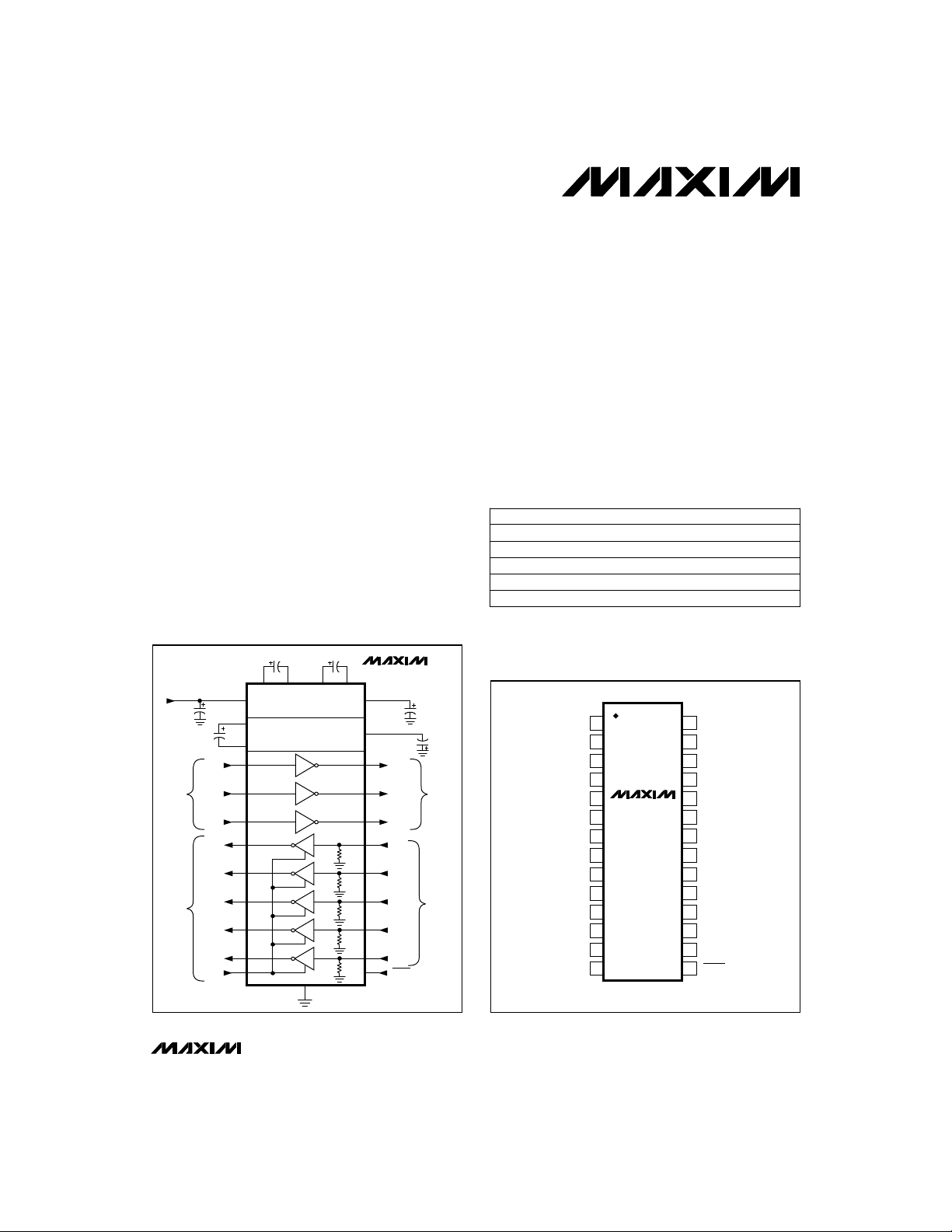
__________Typical Operating Circuit
0.33µF 0.33µF
+2.7V TO
+5.25V
INPUT
CMOS
INPUTS
CMOS
OUTPUTS
0.33µF
R1
R2
R3
R4
R5
0.33µF
T1
IN
T2
IN
T3
IN
OUT
OUT
OUT
OUT
OUT
EN
2
C1A C1B
C1A+ C1A- C1B+ C1B-
1
V
CC
DOUBLER/TRIPLER
25
C2+
C2
24
C2-
11
12
13
6
7
8
9
10
14
VOLTAGE
VOLTAGE
INVERTER
T1
T2
T3
R1
R2
R3
R4
R5
GND
27
MAX562
453
28
V+
C3 0.68µF
26
V-
5k
5k
5k
5k
5k
18
17
16
23
22
21
20
19
15
C4 0.33µF
T1
OUT
T2
OUT
T3
OUT
R1
IN
R2
IN
R3
IN
R4
IN
R5
IN
SHDN
EIA/TIA
-562
OUTPUTS
EIA/TIA
-562
INPUTS
____________________________Features
♦ 230kbps Data Rate, LapLink™ Compatible
♦ Operates from a 2.7V to 5.25V Supply
♦ Designed for EIA/TIA-562 and EIA/TIA-232 Applications
♦ Guaranteed 4.0V/µs Slew Rate
♦ 3 Drivers, 5 Receivers
♦ Flow Through Pinout
♦ Low-Power Shutdown and Keep-Awake Modes
♦ Low-Cost, Surface-Mount External Capacitors
______________Ordering Information
PART TEMP. RANGE PIN-PACKAGE
MAX562CWI 0°C to +70°C 28 SO
MAX562CAI 0°C to +70°C 28 SSOP
MAX562C/D 0°C to +70°C Dice*
MAX562EWI -40°C to +85°C 28 SO
MAX562EAI -40°C to +85°C 28 SSOP
* Contact factory for dice specifications.
__________________Pin Configuration
TOP VIEW
V+
28
GND
27
V-
26
C2+
25
C2-
24
R1
23
IN
22
R2
IN
21
R3
IN
20
R4
IN
19
R5
IN
18
T1
OUT
T2
17
OUT
T3
16
OUT
15
SHDN
C1A+
C1B+
C1BC1A-
R1
R2
R3
R4
R5
1
V
CC
2
3
4
5
OUT
OUT
OUT
OUT
OUT
T1
T2
T3
EN
MAX562
6
7
8
9
10
IN
11
12
IN
13
IN
14
SO/SSOP
MAX562
™ LapLink is a registered trademark of Traveling Software, Inc.
________________________________________________________________
Maxim Integrated Products
Call toll free 1-800-998-8800 for free samples or literature.
1
Page 2
Complete 230kbps, 2.7V to 5.25V
Serial Interface for Notebook Computers
ABSOLUTE MAXIMUM RATINGS
VCC......................................................................... -0.3V to +6V
V+ ................................................................ (V
V-............................................................................ +0.3V to -6V
C1A+, C1B+.................................................. -6V to (V+ + 0.3V)
C1A-, C1B-, C2+........................................ -0.3V to (V+ + 0.3V)
C2-.................................................................. (V- - 0.3V) to +6V
Input Voltages
MAX562
T
, EN,
SHDN
IN
R
....................................................................................±25V
IN
Output Voltages
T
OUT
R
OUT
Stresses beyond those listed under “Absolute Maximum Ratings” may cause permanent damage to the device. These are stress ratings only, and functional
operation of the device at these or any other conditions beyond those indicated in the operational sections of the specifications is not implied. Exposure to
absolute maximum rating conditions for extended periods may affect device reliability.
........................................ -0.3V to (VCC+ 0.3V)
............................................................................... ±15V
...................................................... -0.3V to (VCC+ 0.3V)
- 0.3V) to +6V
CC
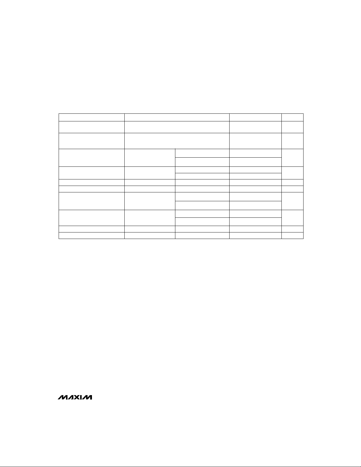
ELECTRICAL CHARACTERISTICS
(VCC= 2.7V to 5.25V, C1A = C1B = C2 = C4 = 0.33µF, C3 = 0.68µF, TA= T
PARAMETER MIN TYP MAX UNITS
EIA/TIA-562 TRANSMITTERS
Output Voltage Swing All transmitter outputs loaded with 3kΩ to GND ±3.7 ±4.5 ±6.0 V
Input Logic Threshold Low
Input Logic Threshold High
Output Leakage Current ±10 µA
Output Resistance VCC= V+ = V- = 0V, V
Output Short-Circuit Current V
EIA/TIA-562 RECEIVERS
Input Voltage Operating Range ±25 V
Input Threshold Low 0.8 V
Input Threshold High 2.4 V
Input Hysteresis
Input Resistance -15V < VIN< 15V 3 5 7 kΩ
Output Voltage Low I
Output Voltage High I
Output Leakage Current
POWER SUPPLY
Operating Supply Voltage 2.7 5.25 V
VCCPower-Supply Current VCC= 3.3V
Shutdown Supply Current with
Receivers Active
Shutdown Supply Current
TIN, EN,
SHDN
TIN, EN,
SHDN
= 0V ±60 mA
OUT
No hysteresis when
= 1.6mA 0.4 V
OUT
= -1.0mA V
OUT
EN = GND, 0V ≤ R
EN = VCC,
SHDN
= EN = GND, TA= +25°C
CONDITIONS
OUT
SHDN
≤ V
OUT
SHDN
= GND, TA= +25°C
Short-Circuit Duration
to GND........................................................ Continuous
T
OUT
R
to GND, VCC................................................ Continuous
OUT
Continuous Power Dissipation (T
SO (derate 12.50mW/°C above +70°C).................. 1000mW
SSOP (derate 9.52mW/°C above +70°C) ................. 762mW
Operating Temperature Ranges:
MAX562C_ _ ..................................................... 0°C to +70°C
MAX562E_ _ .................................................. -40°C to +85°C
Storage Temperature Range........................... -65°C to +160°C
Lead Temperature (soldering, 10sec)........................... +300°C
to T
MIN
VCC= 2.7V to 3.6V 0.6
VCC= 5.0V +5%, -10% 0.8
VCC= 2.7V to 3.6V 1.8
VCC= 5.0V +5%, -10% 3.0
= ±2V 300 Ω
= 0V
CC
No load 20 33
All outputs loaded 3kΩ 24
, unless otherwise noted.)
MAX
VCC-0.5
= +70°C)
A
0.3 V
0.05 ±10 µA
45 130 µA
1 50 µA
mA
V
V
2 _______________________________________________________________________________________
Page 3
Complete 230kbps, 2.7V to 5.25V
Serial Interface for Notebook Computers
AC CHARACTERISTICS
PARAMETER CONDITIONS MIN TYP MAX UNITS
Data Rate
Transmitter Slew Rate
Transmitter Rise/Fall Time
Transmitter Propagation Delay
Transmitter-Output Enable Time 100 µs
Transmitter-Output Disable Time Figure 3 600 ns
Receiver Propagation Delay,
Normal Operation
Receiver Propagation Delay,
Keep-Awake Mode
Receiver-Output Enable Time Figure 4 100 250 ns
Receiver-Output Disable Time Figure 4 250 500 ns
1000pF || 3kΩ load each transmitter output,
150pF load each receiver output
CL= 50pF to 2500pF,
RL= 3kΩ to 7kΩ. Measured from +3V to -3V, or
-3V to +3V
RL= 3kΩ measured
from +3.3V to -3.3V
or -3.3V to +3.3V
2500pF || 3kΩ load,
Figure 1
CL= 150pF,
SHDN
= VCCFigure 2
CL= 150pF,
SHDN
= GND
Figure 2
CL= 2500pF 0.22 3.1
CL= 1000pF 0.22 2.1
t
PHLT
t
PLHT
t
ET
t
DT
t
PHLR
t
PLHR
t
PHLS
t
PLHS
t
ER
t
DR
230.4 280.0 kbits/sec
4 6 30 V/µs
900 1700
1000 1700
100 250
250 500
3000 4000
2000 3000
MAX562
µs
ns
ns
ns
_______________________________________________________________________________________ 3
Page 4

Complete 230kbps, 2.7V to 5.25V
Serial Interface for Notebook Computers
__________________________________________Typical Operating Characteristics
__________________________________________Typical Operating Characteristics
(VCC= 3.3V, C1A = C1B = C2 = C4 = 0.33µF, C3 = 0.68µF, TA=+25°C, unless otherwise noted.)
TRANSMITTER SLEW RATE
vs. LOAD CAPACITANCE
8.0
7.5
MAX562
7.0
6.5
6.0
5.5
SLEW RATE (V/µs)
5.0
4.5
4.0
0 2000 3000 4000 5000
1000
SUPPLY CURRENT
vs. SUPPLY VOLTAGE
38
36
34
32
30
28
26
SUPPLY CURRENT (mA)
24
22
20
2.5 3.5 4.0
3.0
ALL OUTPUTS LOADED
C
ALL TRANSMITTERS LOADED 3kΩ
V
L
CC
3kΩ II C
SLEW+
SLEW-
(pF)
(V)
L
4.5 5.0 5.5
TRANSMITTER OUTPUT VOLTAGE
vs. TEMPERATURE
6
5
4
3
2
1
0
-1
-2
-3
-4
TRANSMITTER OUTPUT VOLTAGE (V-, V+)
-5
-6
-40
38
36
34
32
30
28
SUPPLY CURRENT (mA)
26
24
22
-40
60
SHDN = 0, EN = 1
ALL TRANSMITTERS LOADED 3kΩ
55
T_
+
OUT
+3.7V EIA/TIA-562
ALL TRANSMITTERS LOADED 3kΩ
-3.7V EIA/TIA-562
T_
-
OUT
0
40
TEMPERATURE (°C)
SUPPLY CURRENT
vs. TEMPERATURE
VCC = +2.7V
ALL TRANSMITTERS LOADED 3kΩ
VCC = +3.3V
0
40
TEMPERATURE (°C)
SUPPLY CURRENT
vs. TEMPERATURE
TRANSMITTER OUTPUT VOLTAGE
vs. LOAD CAPACITANCE, TO 231kbps
6
5
.....
.....
80
4
3
2
1
0
-1
-2
-3
-4
TRANSMITTER OUTPUT VOLTAGE (V-, V+)
-5
-6
0 2000 3000 4000 5000
vs. TRANSMITTER DATA RATE
55
50
45
3 OUTPUTS LOADED
40
35
30
SUPPLY CURRENT (mA)
25
20
80
0
T_
ALL TRANSMITTERS
LOADED 3kΩ II C
T_
1000
C
SUPPLY CURRENT
3kΩ II 2500pF
1 OUTPUT LOADED
3kΩ II 2500pF
100
50
DATA RATE (kbps)
+
OUT
-
OUT
(pF)
L
2 OUTPUTS LOADED
3kΩ II 2500pF
150
L
200 250
50
45
SUPPLY CURRENT (µA)
40
35
-40
4
_______________________________________________________________________________________
VCC = +3.3V
VCC = +2.7V
0
40
TEMPERATURE (°C)
80
Page 5

Complete 230kbps, 2.7V to 5.25V
Serial Interface for Notebook Computers
______________________________________________________________Pin Description
PIN NAME FUNCTION
28
2, 5 C1A+, C1A- Terminals for positive charge-pump capacitor
3, 4 C1B+, C1B- Terminals for positive charge-pump capacitor
6, 7, 8, 9, 10 R_
11, 12, 13 T_
14 EN Receiver Enable, see
15
16, 17, 18 T_
19, 20, 21, 22, 23 R_
24, 25 C2+, C2- Terminals for negative charge-pump capacitor
26 V- Negative charge-pump output, typically -5.2V
27 GND Ground
1V
V+ Positive charge-pump output, typically 5.8V
OUT
IN
TTL/CMOS Receiver Outputs.
TTL/CMOS Driver Inputs
Shutdown and Enable Control
SHDN
OUT
IN
CC
Shutdown Control, see
EIA/TIA-562 Driver Outputs
EIA/TIA-562 Receiver Inputs
+2.7V to +5.25V Supply Voltage
Shutdown and Enable Control
section.
section.
MAX562
+3V
INPUT
OUTPUT
t
PLHT
0V
Figure 1. Transmitter Propagation Delay Timing
_______________________________________________________________________________________ 5
t
PHLT
+3V
INPUT
V
OH
0V
V
OL
OUTPUT
t
PHLR
t
PHLS
50%
50%
50%
50%
GND
t
PLHR
t
PLHS
0V
V
CC
Figure 2. Receiver Propagation Delay Timing
Page 6

Complete 230kbps, 2.7V to 5.25V
Serial Interface for Notebook Computers
+3V
SHDN
0V
V
MAX562
A. TIMING DIAGRAM
B. TEST CIRCUIT
OH
TRANSMITTER
OUTPUTS
V
OL
1 OR 0 T
X
OUTPUT DISABLE TIME (tDT)
+3V
0V
-3V
3k
50pF
Figure 3. Transmitter-Output Disable Timing
_______________Detailed Description
The MAX562 has three sections: the charge-pump voltage
converter, the drivers (transmitters), and the receivers.
Charge-Pump Voltage Converter
The charge-pump voltage converter is used to produce a
positive and a negative supply to drive the transmitters. The
positive voltage (V+) is generated by a regulated charge
pump working as either a doubler or a tripler (depending on
the VCClevel) and using capacitors C1A, C1B and C3 (see
Typical Operating Circuit
from V+ using a simple charge-pump inverter that employs
capacitors C2 and C4.
These charge-pump converters are regulated to give output
voltages of +5.8V and -5.2V. Having regulated supplies
generated on-chip makes the MAX562's performance insensitive to variations in V
ing changes, and operating temperature changes.
SHDN
When
is low, the charge pumps are disabled, V+ is
internally connected to VCC, and V- is internally connected to
GND.
). The negative voltage (V-) derives
from 2.7V to 5.25V, transmitter load-
CC
EN
R_
IN
A. TEST CIRCUIT
EN INPUT
RECEIVER
OUTPUTS
B. ENABLE TIMING
EN INPUT
RECEIVER
OUTPUTS
C. DISABLE TIMING
V
V
R_
1k
OUT
R_
+3V
0V
OH
OL
150pF
0V
OUTPUT ENABLE TIME (t
V
OH
V
OL
+3V
OUTPUT DISABLE TIME (tDR)
V
VOL +0.5V
OH
-0.5V
-1V,
V
OH
+1.6V
V
OL
EN
EN
)
ER
Figure 4. Receiver-Output Enable and Disable Timing
EIA/TIA-562 Drivers
The driver output voltage is guaranteed to meet the ±3.7V
EIA/TIA-562 specification over the full range of operating
temperatures and voltages, when each transmitter is
loaded with up to 3kΩ and operated up to 230kbps (see
Typical Operating Characteristics
). The typical driver output voltage swing exceeds ±4V with a 3kΩ load on all
transmitter outputs. The open-circuit output voltage swing
is typically from (V+ - 0.7V) to (V- + 0.7V). Output swing is
not significantly dependent on VCCsince the charge
pumps are regulated.
Input thresholds are CMOS and TTL compatible. Connect
unused inputs to V
SHDN
When
is low, the driver outputs are off and their leak-
or to GND.
CC
age currents are less than 10µA, even if the transmitter
outputs are back-driven between -7V and +15V. Taking
SHDN
low does not disable the receivers.
SHDN
When
and EN are both low, the entire chip is
disabled and all outputs are high impedance. Power
consumption is lowest in this condition. Exiting shutdown
takes about 100µs, but depends on VCC. Figure 5 shows
6 _______________________________________________________________________________________
Page 7

Complete 230kbps, 2.7V to 5.25V
SHDN
Serial Interface for Notebook Computers
5
0
6
4
2
VOLTS (V)
0
-2
-4
Figure 5. Time for Transmitters to Exit Shutdown
the MAX562 transmitter outputs when
transmitter outputs are shown going to opposite EIA/TIA562 levels (one transmitter input is high, the other is low).
Each transmitter is loaded with 3kΩ in parallel with
2500pF. The transmitter outputs are well behaved, with
no ringing or undesirable transients as they come out of
shutdown.
Each transmitter is designed to drive a single receiver.
Transmitters can be paralleled to drive multiple
receivers.
All 5 receivers are identical and accept EIA/TIA-562 or
EIA/TIA-232 signals. The CMOS receiver outputs swing
between VCCand GND. They are inverting, maintaining
compatibility with the driver outputs.
SHDN
VCC = +2.2V VCC = +2.7V VCC = +5.0VVCC = +3.3V
0
TIME (µs)
Driving Multiple Receivers
EIA/TIA-562 Receivers
200 300100
SHDN
rises. Two
The guaranteed 0.8V and 2.4V receiver input thresholds are significantly tighter than the ±3.0V thresholds
required by the EIA/TIA-562 specification. This allows
the receiver inputs to respond to TTL/CMOS logic levels as well as EIA/TIA-562/232 levels. Also, the
MAX562's guaranteed 0.8V lower threshold ensures
that receivers shorted to ground will have a logic 1 output. The 5kΩ input resistance to ground ensures that a
receiver with its input left open will also have a logic 1
output.
The receiver inputs have approximately 0.3V hysteresis
SHDN
when
is high. This provides clean output transitions, even with slowly moving input signals with moderate noise and ringing.
The receivers are active when EN is high. When EN is
low, the receiver outputs are high impedance. This
allows wire-OR connection of two EIA/TIA-562 ports (or
ports of different types) at the UART.
The receivers are always active,when EN is high, irrespective of
SHDN
's state. When
SHDN
is high, the
receivers have hysteresis and experience the shortest
propagation delays (typically 100ns falling, 250ns rising). When
SHDN
is low, the receivers have longer
propagation delays (typically 3µs falling, 2µs rising)
and have no hysteresis. The receiver outputs are not
valid for 50µs after
SHDN
goes low.
Shutdown and Enable Control
SHDN
and EN determine the operation of the MAX562
as shown in Table 1.
__________Applications Information
Capacitor Selection
The capacitor type is not critical for proper MAX562
operation. Any low cost ceramic capacitor (e.g., Z5U,
Y5V) is acceptable for operating at room temperature,
MAX562
Table 1. MAX562 Control Pin Configurations
EN
CHARGE-PUMP
OPERATION
STATUS
0 0 Shutdown High-Z High-Z 1µ
0 1 Shutdown High-Z Active* 45µ
1 0 Normal Operation Active High-Z 24m
1 1 Normal Operation Active Active 24m
* Active, but with reduced performance (see
_______________________________________________________________________________________ 7
EIA/TIA-562 Receivers
TRANSMITTERS
T1-T3
section). This is “keep-awake” mode.
RECEIVERS
R1-R5
SUPPLY
CURRENT
TYP (A)
Page 8

Complete 230kbps, 2.7V to 5.25V
Serial Interface for Notebook Computers
Table 2. Summary of EIA/TIA-232E/V.28 and EIA/TIA-562 Specifications
PARAMETER CONDITION
Driver Output Voltage
0 Level
1 Level -5.0V to -15.0V -3.7V to -13.2V
MAX562
3kΩ to 7kΩ load
EIA/TIA-232E/V.28
SPECIFICATION
5.0V to 15.0V 3.7V to 13.2V
Maximum Output Level No load ±25V ±13.2V
= 2500pF Up to 20kbps Up to 20kbps
C
Signal Rate (3kΩ ≤ R
≤ 7kΩ)
L
and X7R ceramic capacitors are recommended for
L
= 1000pF Not defined Up to 64kbps
C
L
___________________Chip Topography
operation over the full temperature range.
Larger capacitors may be used for C2 and C4 (see
Typical Operating Circuit
) to reduce ripple on the trans-
mitter output voltages.
C1B+
C1A+
32128 27 26 25
V
CC
GNDV-C2+
V+
Power-Supply Decoupling
In applications that are sensitive to power-supply noise,
decouple VCCto ground with a capacitor similar in
value to that of the C1A and C1B charge-pump capacitors. Connect the bypass capacitor as close as possible to the VCCand GND pins.
C1B-
C1A-
4
5
V+ and V- as Power Supplies
A small amount of power can be drawn from V+ and V-.
Excessive loads will cause V+ and V- to fall out of
regulation. When V+ or V- are loaded, check for good
regulation over the intended operating temperature
range.
R1
R2
R3
R4
R5
OUT
OUT
OUT
OUT
OUT
6
7
8
9
10
EIA/TIA-562
SPECIFICATION
24
23
22
21
20
19
C2-
0.164"
(4.166mm)
R1
IN
R2
IN
R3
IN
R4
IN
R5
IN
11 12 13 14 15 16 17 18
T2
EN
IN
T1
T3
IN
IN
T3
SHDN
0.135"
(3.429mm)
OUT
T1
OUT
T2
OUT
Substrate connected to V+
Transistor count: 1892
Maxim cannot assume responsibility for use of any circuitry other than circuitry entirely embodied in a Maxim product. No circuit patent licenses are
implied. Maxim reserves the right to change the circuitry and specifications without notice at any time.
8
___________________Maxim Integrated Products, 120 San Gabriel Drive, Sunnyvale, CA 94086 (408) 737-7600
© 1993 Maxim Integrated Products Printed USA is a registered trademark of Maxim Integrated Products.
 Loading...