

Page 1
General Description
The MAX5486 dual 40kΩ logarithmic taper volume control features a debounced pushbutton up/down interface
that controls volume and balance in audio applications.
Each potentiometer has 32 log-spaced tap points with a
buffered wiper output to replace mechanical potentiometers. An integrated bias generator provides the required
((V
DD
+ VSS) / 2) bias voltage, eliminating the need for
costly external op-amp circuits in unipolar audio applications. A mode-indicator LED output indicates volume or
balance control. Five integrated LED drivers indicate volume level or balance settings, depending on the status of
the mode indicator.
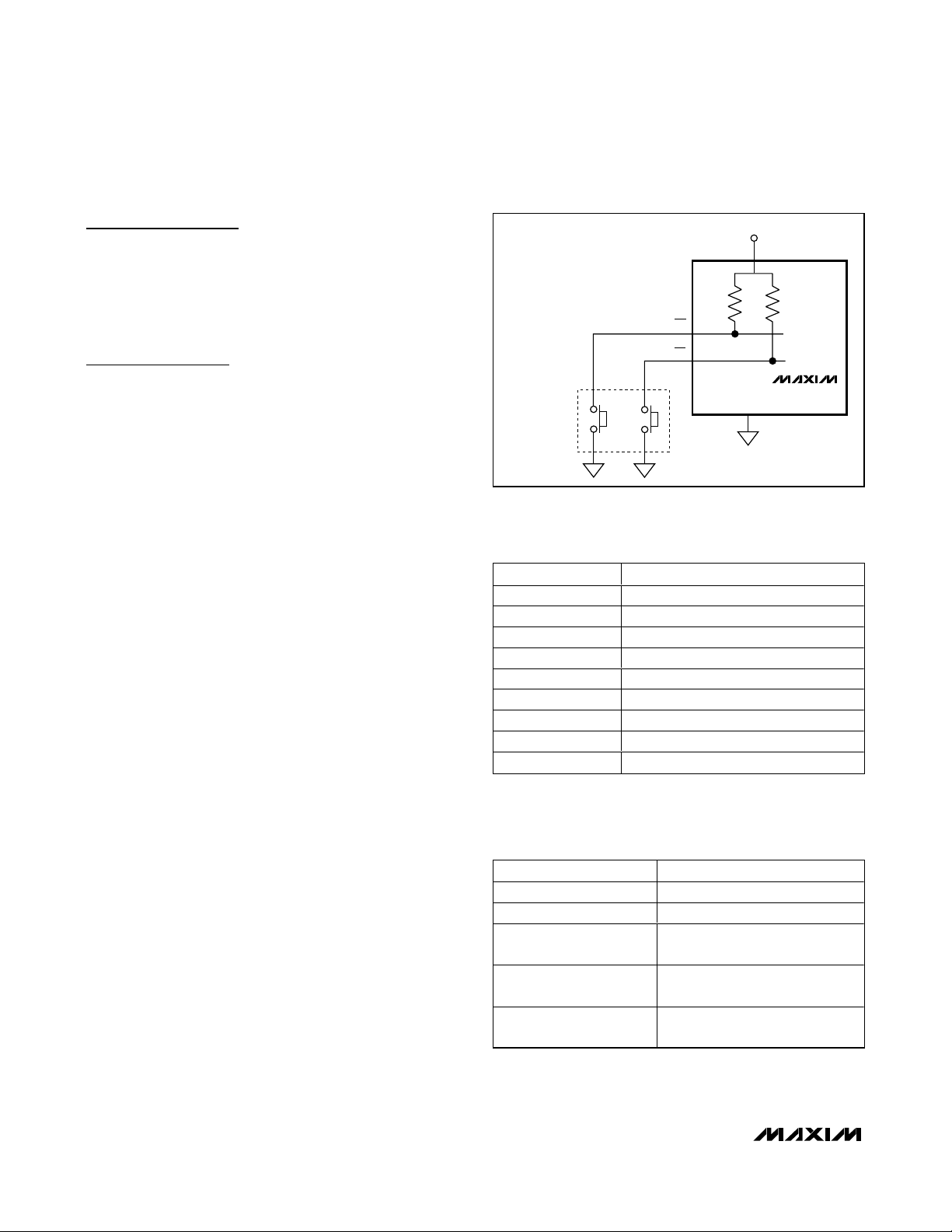
Use the MAX5486 digital inputs with momentary contact single-pole/single-throw (SPST) pushbutton switches. Each input includes internal debounced circuitry
and a pullup resistor to V
LOGIC
.
The MAX5486 advances the wiper setting once per button push. Maxim’s proprietary SmartWiper™ control
eliminates the need for a microcomputer to increase the
wiper transition rate. The accelerated auto-advance
feature provides a wiper-changing rate at 4Hz for holding the control input low for more than 250ms and at
8Hz after 500ms and then at 11Hz after 1000ms (see
Table 2).
All of the MAX5486’s pushbutton inputs are debounced.
The mute input allows a single pushbutton to change
between volume control and the -90dB (typ) mute setting. The mode input toggles between volume and balance control. The click-and-pop suppression feature
minimizes the audible noise generated by wiper transitions. The typical total harmonic distortion plus noise
(THD+N) for the device is 0.003%. The MAX5486 provides a nominal temperature coefficient of 35ppm/°C
end-to-end and 5ppm/°C ratiometrically and a nominal
resistance of 40kΩ per potentiometer. The MAX5486 is
available in a 24-pin TSSOP package and is specified
for operation over the -40°C to +85°C extended temperature range.
Applications
Home-Theater Speakers
Desktop Speakers
Portable Media Players
Docking Stations
Automotive Rear-Seat Multimedia
Features
♦ Debounced Pushbutton Interface
♦ SmartWiper Control Advances Wiper Rate
♦ Low-Power Wiper Buffers Provide 0.003% THD+N
♦ Bias Generator Eliminates External Op Amps
♦ Five-Segment LED Volume/Balance Indicator
♦ Clickless Switching
♦ Logarithmic Taper Volume Control with (31)
2dB Steps
♦ Single +2.7V to +5.5V or Dual ±2.7V Supply
Voltage Operation
♦ Power-On Reset to -12dBFS Wiper Position
♦ MUTE Function Toggles to 90dB (typ)
♦ Low 1µA Shutdown Supply Current
♦ 40kΩ End-to-End Fixed Resistance Value
♦ Small, 24-Pin TSSOP Package
MAX5486
Stereo Volume Control with Pushbutton
Interface
________________________________________________________________
Maxim Integrated Products
1
19-0672; Rev 0; 11/06
For pricing, delivery, and ordering information, please contact Maxim/Dallas Direct! at
1-888-629-4642, or visit Maxim’s website at www.maxim-ic.com.
Ordering Information
V
DD
V
SS
(V
DD + VSS
) / 2
(V
DD + VSS
) / 2
V
LOGIC
V
PEAK
HR
L
R
WR
SHDN
LEFT INPUT
RIGHT INPUT
MODEIND
MAX9761
LL
HL
WL
V
LOGIC
LEDIND4
LEDIND3
LEDIND0
GND
MUTE
LEDIND1
LEDIND2
BIAS
BIASCAP
MAX5486
UP/BALL
DN/BALR
MODE
1MΩ
(V
DD + VSS
) / 2
V
PEAK
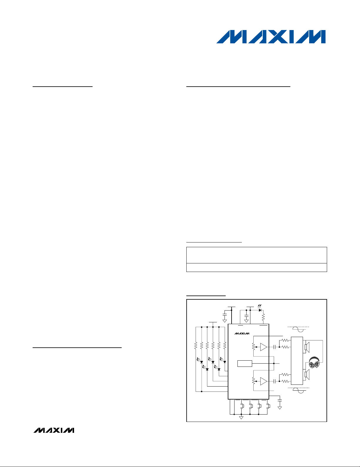
Typical Operating Circuit
SmartWiper is a trademark of Maxim Integrated Products, Inc.
+
Denotes lead-free package.
PART TEMP RANGE
MAX5486EUG+ -40°C to +85°C 24 TSSOP U24-1
PINPACKAGE
PKG
CODE
Page 2
MAX5486
Stereo Volume Control with Pushbutton
Interface
2 _______________________________________________________________________________________
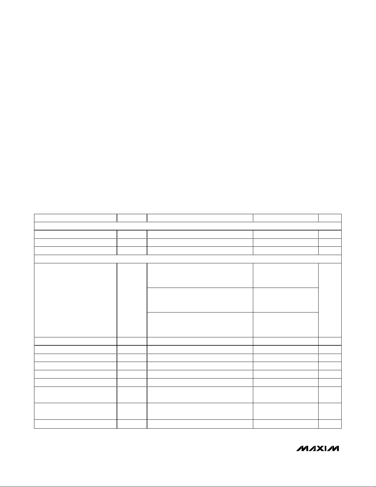
ABSOLUTE MAXIMUM RATINGS
ELECTRICAL CHARACTERISTICS
(VDD= +2.7V to +5.5V, VSS= GND = 0, 2.7V ≤ (VDD- VSS) ≤ 5.5V, C
BIASCAP
= 1µF, BIAS = 3kΩ to GND, V
LOGIC
= +2.7V to VDD,
VH_ = V
DD
- 0.15V, VL_= (VDD- VSS) / 2, SHDN = MUTE = V
LOGIC
, all LED outputs open, pushbutton interface inactive, VH= V
BIAS
+ 1V
RMS
, V
BIAS
= (VDD- VSS) / 2, TA= T
MIN
to T
MAX
, unless otherwise specified. Typical values are at TA= +25°C.) (Note 1)
Stresses beyond those listed under “Absolute Maximum Ratings” may cause permanent damage to the device. These are stress ratings only, and functional
operation of the device at these or any other conditions beyond those indicated in the operational sections of the specifications is not implied. Exposure to
absolute maximum rating conditions for extended periods may affect device reliability.
SHDN, MODE, MUTE, UP/BALL, and DN/BALR to
GND .................-0.3V to the lower of (V
LOGIC
+ 0.3V and +6V)
H_, L_, W_, BIASCAP,
BIAS to GND .........-0.3V to the lower of (V
DD
+ 0.3V and +6V)
LEDIND_, MODEIND to GND...................................-0.3V to +6V
V
LOGIC
to GND.........................................................-0.3V to +6V
V
DD
to GND..............................................................-0.3V to +6V
V
DD
to V
LOGIC
.............................................................-6V to +6V
GND to V
SS
...............................................................-0.3V to +6V
V
DD
to VSS................................................................-0.3V to +6V
Average Current into H_, L_, and W_ .................................±1mA
Maximum Continuous Current into H_, L_ ..........................±4mA
Input and Output Latchup Immunity...............................±200mA
Continuous Power Dissipation (T
A
= +70°C)
24-Pin TSSOP (derate 8.3mW/°C above +70°C) ..........657mW
Operating Temperature Range ...........................-40°C to +85°C
Storage Temperature Range .............................-60°C to +150°C
Maximum Junction Temperature .....................................+150°C
Lead Temperature (soldering, 10s) .................................+300°C
RESISTOR LADDER
End-to-End Resistance R 40 kΩ
Absolute Tolerance ±0.25 dB
Tap-to-Tap Tolerance (Note 2) ±0.1 dB
VOLUME CONTROL
PARAMETER SYMBOL CONDITIONS MIN TYP MAX UNITS
VDD = 5V, VSS = 0, VH = (V
= V
V
L
V
L
/ 2, 1kHz, tap at top, RL = 10kΩ to
DD
= V
/ 2, 20Hz to 20kHz
DD
DD
/ 2) + 1V
RMS
,
0.003
Total Harmonic Distortion Plus
Noise
THD+N
VDD = 5V, VSS = 0, VH = (V
V
= V
L
V
L
V
DD
1.5V
R
L
/ 2, 1kHz, tap at top, RL = ∞Ω to
DD
= V
/ 2, 20Hz to 20kHz
DD
= 5V, VSS = 0, VH = (V
, VL = V
RMS
= 10kΩ to VL = V
/ 2, 1kHz, tap at top,
DD
DD
Channel Isolation VDD = +2.7V, VSS = -2.7V, V
/ 2) + 1V
DD
DD
/ 2) +
RMS
/ 2, 20Hz to 20kHz
= GND 100 dB
BIAS
,
0.001
0.012
Interchannel Matching ±0.5 dB
Mute Attenuation SHDN = V
DD
Power-Supply Rejection Ratio PSRR Input referred, 217Hz, 100mV
H Terminal Capacitance C
L Terminal Capacitance C
H
L
End-to-End Resistance
Temperature Coefficient
Ratiometric Resistance
Temperature Coefficient
Bandwidth, -3dB f
CUTOFFCW
= 50pF 100 kHz
P-P
on V
DD
90 dB
72 dB
5pF
7pF
35 ppm/°C
5 ppm/°C
%
Page 3
MAX5486
Stereo Volume Control with Pushbutton
Interface
_______________________________________________________________________________________ 3
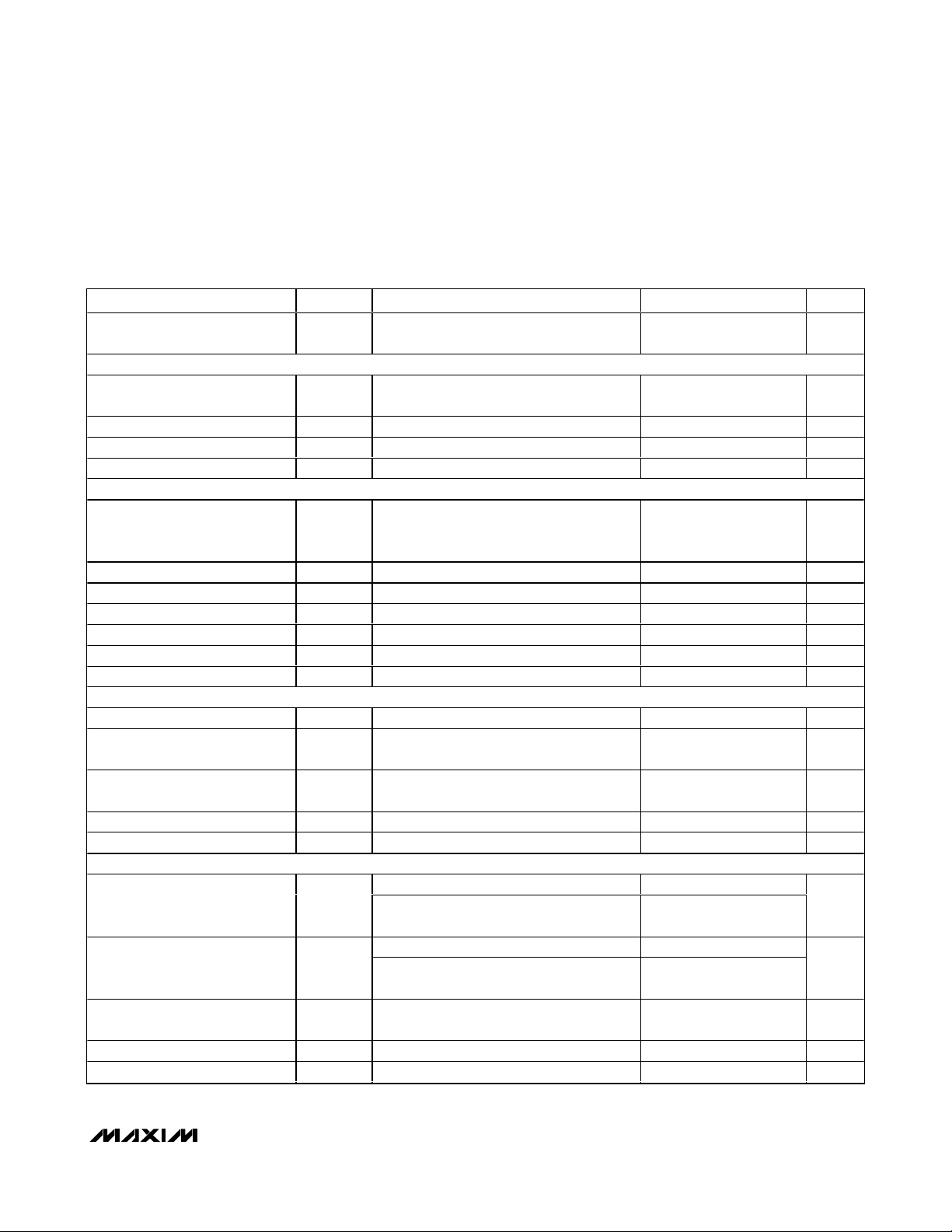
ELECTRICAL CHARACTERISTICS (continued)
(VDD= +2.7V to +5.5V, VSS= GND = 0, 2.7V ≤ (VDD- VSS) ≤ 5.5V, C
BIASCAP
= 1µF, BIAS = 3kΩ to GND, V
LOGIC
= +2.7V to VDD,
VH_ = V
DD
- 0.15V, VL_= (VDD- VSS) / 2, SHDN = MUTE = V
LOGIC
, all LED outputs open, pushbutton interface inactive, VH= V
BIAS
+ 1V
RMS
, V
BIAS
= (VDD- VSS) / 2, TA= T
MIN
to T
MAX
, unless otherwise specified. Typical values are at TA= +25°C.) (Note 1)
PARAMETER SYMBOL CONDITIONS MIN TYP MAX UNITS
Output Noise e
20Hz to 20kHz, VH = VL = V
N
ground, tap = -6dB
DD
/ 2 = AC
2.2 µV
RMS
WIPER BUFFER
Output Voltage Swing V
O
RL = 3kΩ to V
BIAS
VDD -
0.3V
V
Output Current 3mA
Output Resistance R
DC Offset V
OWB
OS
110Ω
±2 ±14 mV
INTEGRATED BIAS GENERATOR
Output Voltage RL > 100kΩ
Power-Supply Rejection Ratio At 1kHz, 100mV
P-P
on V
DD
(V
DD
V
) / 2
SS
- 20mV
+
+
(V
DD
V
) / 2
SS
60 dB
+
(V
DD
V
) / 2
SS
+ 20mV
V
Minimum Load Resistance 3kΩ
Maximum Load Capacitance 100 pF
Output Resistance R
OBR
Noise Voltage 20Hz to 20kHz 2.2 µV
6 Ω
RMS
Minimum Output Current 2mA
CONTACT INPUTS (MUTE, MODE, UP/BALL, DN/BALR)
Internal Pullup Resistor R
Single-Pulse Input Low Time t
Repetitive Input Pulse Separation
Time
Timeout Period t
CPW
t
IPWS
WS
PU
Time required for a single pulse to cause an
increment/decrement
16 ms
1ms
Click-and-pop suppression inactive 126 ms
42 kΩ
Debounce Corner Frequency Internal analog filter 10 kHz
DIGITAL INPUTS (V
Input High Voltage V
Input Low Voltage V
Input Leakage Current
LOGIC
> 4.5V)
V
> 4.5V 2.4
LOGIC
IH
V
< 4.5V
LOGIC
V
> 4.5V 0.8
LOGIC
IL
V
< 4.5V
LOGIC
To GND for inputs with internal pullup
resistors
0.7 x
V
LOGIC
0.3 x
V
LOGIC
±1 µA
V
V
Input Capacitance 5pF
Digital Clock Feedthrough f
= 1Hz to 40Hz, tap = -6dB -90 dB
CLK
Page 4
MAX5486
Stereo Volume Control with Pushbutton
Interface
4 _______________________________________________________________________________________
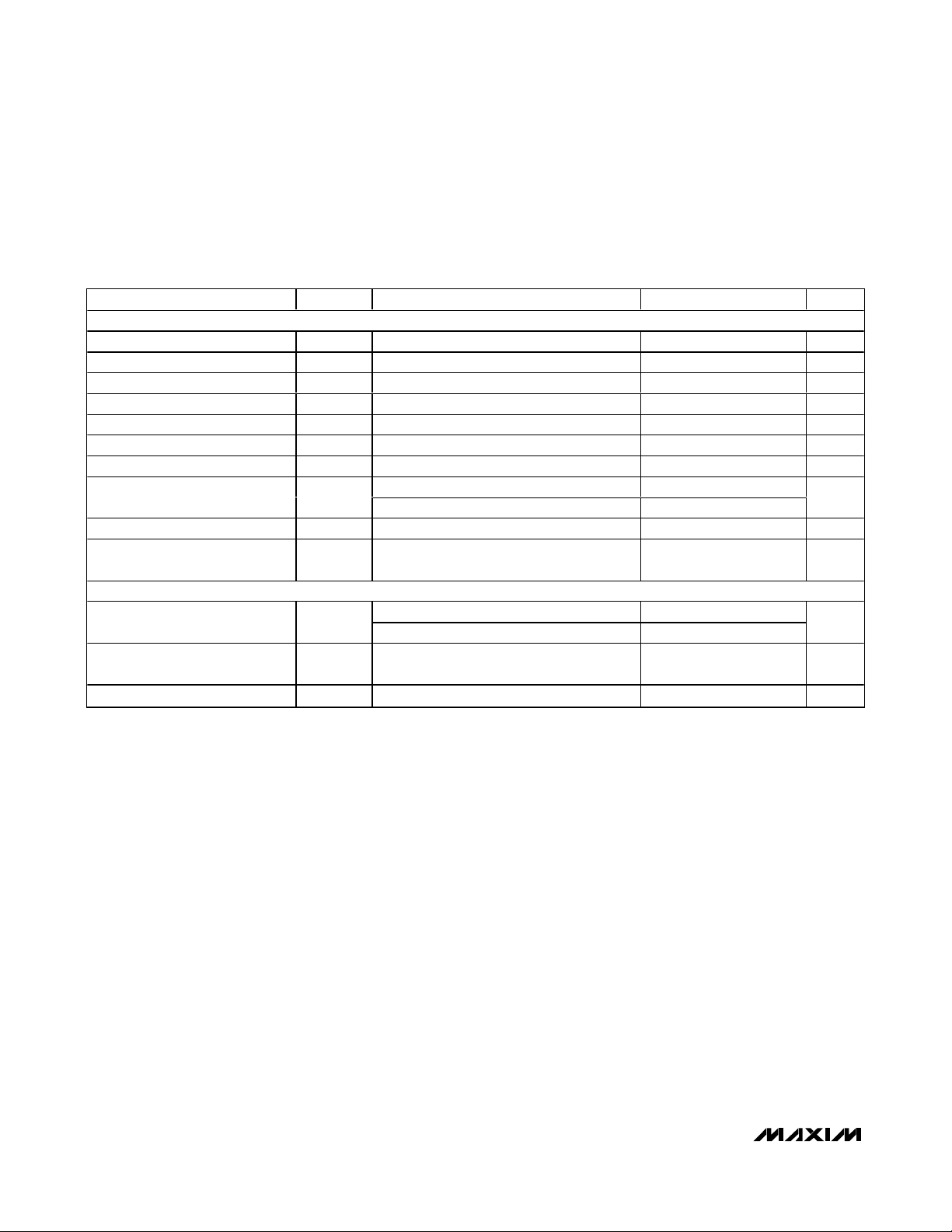
ELECTRICAL CHARACTERISTICS (continued)
(VDD= +2.7V to +5.5V, VSS= GND = 0, 2.7V ≤ (VDD- VSS) ≤ 5.5V, C
BIASCAP
= 1µF, BIAS = 3kΩ to GND, V
LOGIC
= +2.7V to VDD,
VH_ = V
DD
- 0.15V, VL_= (VDD- VSS) / 2, SHDN = MUTE = V
LOGIC
, all LED outputs open, pushbutton interface inactive, VH= V
BIAS
+ 1V
RMS
, V
BIAS
= (VDD- VSS) / 2, TA= T
MIN
to T
MAX
, unless otherwise specified. Typical values are at TA= +25°C.) (Note 1)
Note 1: Parameters are 100% production tested at +85°C and limits through the temperature range are guaranteed by design.
Note 2: Tap-to-tap tolerance is the error in voltage change between successive tap positions.
Note 3: Supply current measured while wiper position is fixed.
Note 4: One button pressed.
POWER SUPPLIES
Positive Power Supply V
Negative Power Supply V
Supply-Voltage Difference VDD - V
Analog Supply Current I
Power-Up Time t
Logic Supply Voltage V
Logic Active Supply Current I
Logic Standby Supply Current
(Note 3)
Shutdown Current I
Shutdown Time/Return from
Shutdown
LED INDICATORS (LEDIND0–LEDIND4, MODEIND)
Output Low Voltage V
Maximum Output Leakage
Current
Output Capacitance 3pF
PARAMETER SYMBOL CONDITIONS MIN TYP MAX UNITS
DD
SS
DD
PU
LOGICVSS
LOGIC
I
LOGICSTBY
SHDN
t
SHDN
OL
VSS = 0 2.7 5.5 V
VDD = +2.7V -2.7 0 V
(Note 3) 1.4 mA
V
LOGIC
VDD = +5V, VSS = 0 1
VDD = +2.7V, VSS = -2.7V 1
SHDN = 0, total of all supplies 1 µA
After 1st zero crossing 1 ms
V
LOGIC
V
LOGIC
SS
= 0 2.7 V
= VDD (Note 4) 200 µA
= 2.7V, I
= 5V, I
= 10mA 0.4
SINK
= 10mA 0.2
SINK
5.5 V
126 ms
DD
10 µA
V
µA
V
Page 5
MAX5486
Stereo Volume Control with Pushbutton
Interface
_______________________________________________________________________________________
5
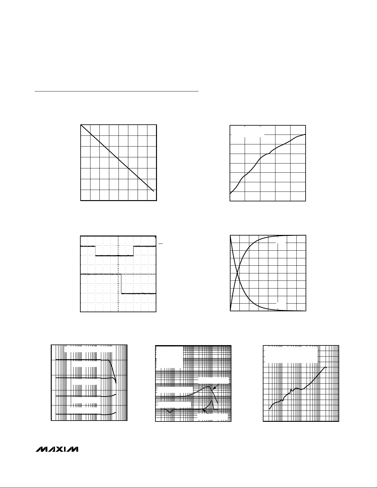
Typical Operating Characteristics
(VDD= +5.0V, VSS= GND = 0, V
LOGIC
= +5.0, VH_= VDD- 0.15V, VL_= VDD/ 2, C
BIASCAP
= 1µF)
ATTENUATION vs. TAP POSITION
0
-10
-20
-30
-40
ATTENUATION (dB)
-50
-60
-70
08124 1620242832
WIPER SWITCHING TRANSIENT
5V/div
200mV/div
MAX5486 toc01
TAP POSITION
MAX5486 toc03
DN
WIPER TRANSITION
FROM -2dB TO -4dB
40ms/div
0.15
0.10
0.05
-0.05
-0.10
-0.15
END-TO-END RESISTANCE CHANGE (%)
-0.20
-0.25
)
HL
NOMINAL END-TO-END VOLTAGE (%V
END-TO-END RESISTANCE % CHANGE
vs. TEMPERATURE
VDD = V
V
0
-40 -15 10 35 60 85
= GND = 0
SS
= 5V
LOGIC
TEMPERATURE (°C)
WIPER-TO-END TERMINAL VOLTAGE
vs. TAP POSITION
100
90
80
70
60
50
40
30
20
10
0
08124 1620242832
TAP POSITION
V
HW
V
WL
MAX5486 toc02
MAX5486 toc04
FREQUENCY RESPONSE
5
0
-5
-10
RESPONSE (dB)
-15
-20
0.01 10.1 10 100 1000
VH1 = 2.5V ±1V
W_ SET TO 0dB
W_ SET TO -6dB
W_ SET TO -12dB
W_ SET TO -18dB
FREQUENCY (kHz)
, VL1 = 2.5V
RMS
MAX5486 toc05
TOTAL HARMONIC DISTORTION
PLUS NOISE vs. FREQUENCY
100
VDD = 5V
= GND
V
SS
10
= 2.5V
V
L_
W_ SET TO 0dB
1
0.1
THD+N (%)
VH_ = 2.5V ±1.5V
0.01
VH_ = 2.5V ±1V
0.001
0.0001
0.01 100
FREQUENCY (kHz)
10kΩ OR NO LOAD
RMS
RMS
10kΩ OR NO LOAD
POWER-SUPPLY REJECTION RATIO
-30
VDD = 5V ±100mV
-35
= 5V, VL_ = 2.5V
V
H_
MAX5486 toc06
1010.1
-40
W_ SET TO -6dB
-45
-50
-55
-60
-65
-70
RESPONSE (dB)
-75
-80
-85
-90
-95
-100
0.01 100
, V
= GND
P-P
SS
FREQUENCY (kHz)
MAX5486 toc07
1010.1
Page 6

MAX5486
Stereo Volume Control with Pushbutton
Interface
6 _______________________________________________________________________________________
Typical Operating Characteristics (continued)
(VDD= +5.0V, VSS= GND = 0, V
LOGIC
= +5.0, VH_= VDD- 0.15V, VL_= VDD/ 2, C
BIASCAP
= 1µF)
140
142
146
144
148
150
-40 10-15 35 60 85
ACTIVE LOGIC SUPPLY CURRENT
vs. TEMPERATURE
MAX5486 toc10
TEMPERATURE (°C)
ACTIVE I
LOGIC
(μA)
VDD = V
LOGIC
= 5.5V
2.0
1.5
1.0
0.5
0
0312 456
ACTIVE SUPPLY CURRENT
vs. SUPPLY VOLTAGE
MAX5486 toc11
SUPPLY VOLTAGE (V)
ACTIVE SUPPLY CURRENT (mA)
UP = 0
V
LOGIC
= 5.5V
ACTIVE SUPPLY CURRENT
vs. TEMPERATURE
MAX5486 toc12
TEMPERATURE (°C)
ACTIVE SUPPLY CURRENT (mA)
603510-15
0.5
1.0
1.5
2.0
0
-40 85
VDD = V
LOGIC
= 5.5V
UP = 0
SPECTRAL NOISE DENSITY
MAX5486 toc13
FREQUENCY (kHz)
1010.1
50
100
150
200
250
300
0
0.01 100
NOISE (nV/√Hz)
CROSSTALK vs. FREQUENCY
MAX5486 toc14
FREQUENCY (Hz)
CROSSTALK (dB)
1010.1
-140
-120
-100
-80
-60
-40
-20
0
-160
0.01 100
VDD = 2.7V, VSS = -2.7V, V
LOGIC
= 5V
W_SET TO 0dB, V
HR
= 1V
RMS
VLR = VLL = VHL = 0V
500ns/div
DIGITAL FEEDTHROUGH
50μV/div
WIPER
OUTPUT
MAX5486 toc15
2V/div
PUSHBUTTON
INPUT
0
20
40
60
80
100
120
140
160
2.5 3.53.0 4.0 4.5 5.0 5.5
LOGIC SUPPLY CURRENT
vs. LOGIC SUPPLY VOLTAGE
MAX5486 toc08
LOGIC SUPPLY VOLTAGE (V)
LOGIC SUPPLY CURRENT (μA)
ACTIVE CURRENT
STANDBY CURRENT
LOGIC SUPPLY CURRENT
vs. LOGIC INPUT VOLTAGE
MAX5486 toc09
LOGIC INPUT VOLTAGE (V)
LOGIC SUPPLY CUURENT (μA)
4.54.03.53.02.52.01.51.00.5
100
1000
10
05.0
Page 7

MAX5486
Stereo Volume Control with Pushbutton
Interface
_______________________________________________________________________________________ 7
_______________________________________________________________________________________
7
Pin Description
PIN NAME FUNCTION
1V
2 DN/BALR
3 UP/BALL
4 MUTE
5 MODE
6 SHDN
7 N.C. Internally connected. Leave unconnected.
8 HR Potentiometer R High Terminal
9 LR Potentiometer R Low Terminal
10 WR Potentiometer R Wiper Buffered Output
11 BIAS Midbias Voltage Output. V
12 BIASCAP Bias Generator Bypass. Connect a 1µF filter capacitor from BIASCAP to VSS.
13 V
14 V
15 WL Potentiometer L Wiper Buffered Output
16 LL Potentiometer L Low Terminal
17 HL Potentiometer L High Terminal
18–22
23 MODEIND
24 GND Ground
LOGIC
DD
SS
LEDIND0–
LEDIND4
Digital Logic Power Supply. Bypass V
the device.
Active-Low Downward Volume/Balance Control. Press DN/BALR to decrease the volume in volume
mode and move balance to the right in balance mode. DN/BALR is internally pulled high with a
resistor to V
Active-Low Upward Volume/Balance Control. Press UP/BALL to increase the volume in volume mode
and move balance to the left in balance mode. UP/BALL is internally pulled high with a resistor to
.
V
LOGIC
Active-Low Mute Input. Pull MUTE low to toggle the wiper between the mute setting (see Table 1) and
the current setting. MUTE is internally pulled up to V
Active-Low Volume/Balance Control Input. Each high-to-low transition on MODE toggles between the
volume and balance modes. MODE is pulled high internally with a resistor to V
the MAX5486 is in volume control mode.
Active-Low Shutdown Input. Drive SHDN low to place the device in shutdown mode. In shutdown
mode, the MAX5486 stores the last wiper settings. The wipers move to the L_ end of the resistor
string. Terminating the shutdown mode restores the wipers to the previous settings.
Analog Power Supply. Bypass VDD to ground with a 0.1µF capacitor as close as possible to the
device.
Negative Power Supply. Bypass VSS to ground with a 0.1µF capacitor as close as possible to the
device. Connect to GND for single supply operation.
LED Indicator Open-Drain Output 0–LED Indicator Open-Drain Output 4. Connect a 1MΩ resistor
from LEDIND4 to V
indication of the current volume or balance. In volume mode, all LEDs off indicate mute and all LEDs
on indicate maximum volume. In balanced mode, LED2 on indicates centered or balanced. Connect
LEDIND0–LEDIND4 to GND when LED indicator drivers are not used.
Active-Low Volume-Control/Balance-Control Mode-Indicator Open-Drain Output. Connect to an LED
through a resistor to V
LED is off, the MAX5486 is in volume-control mode.
LOGIC
.
= (VDD + VSS) / 2; connect a 100pF capacitor from BIAS to VSS.
BIAS
to enable these LED inductor drivers. LEDIND0–LEDIND4 form a bar graph
LOGIC
. When the LED is on, the MAX5486 is in balance-control mode. When the
LOGIC
to ground with a 0.1µF capacitor as close as possible to
LOGIC
with a resistor.
LOGIC
. On power-up,
LOGIC
Page 8
MAX5486
Stereo Volume Control with Pushbutton
Interface
8 _______________________________________________________________________________________8 _______________________________________________________________________________________
Detailed Description
The MAX5486 dual 40kΩ logarithmic taper digital volume control features a debounced pushbutton interface
that controls volume and balance in audio applications.
Each potentiometer has 32 log-spaced tap points with
a buffered wiper output and replaces mechanical
potentiometers.
Mode Control (
MODE
)
The MAX5486 MODE input toggles between volume
and balance modes. Each time MODE is forced low,
the device switches between volume and balance
modes. For example, driving MODE low once while in
volume-control mode switches the MAX5486 to balance
mode. Driving MODE low again switches the MAX5486
back to volume mode. MODE is internally pulled high
with a resistor to V
LOGIC
. The MAX5486 powers up in
volume-control mode. Leave unconnected or connect
to V
LOGIC
if balance mode is not required.
Up-and-Down Interface
The MAX5486 interfaces with momentary contact SPST
switches. All switch inputs are internally debounced and
pulled up to V
LOGIC
through resistors. The wiper setting
advances once per button press up to 250ms. Maxim’s
SmartWiper control circuitry allows the wiper to advance
at a 4Hz rate after holding the button for approximately
250ms. After 500ms, the wiper moves at an 8Hz rate.
After 1s, the rate increases to 11Hz (see Table 2). The
SmartWiper control eliminates the need for a microcomputer to increase the wiper transition rate.
The MAX5486 MODE input toggles the part between volume and balance-control modes. The UP/BALL and
DN/BALR inputs control the wiper according to the
selected mode. MODE is internally pulled high with a
resistor to V
LOGIC
.
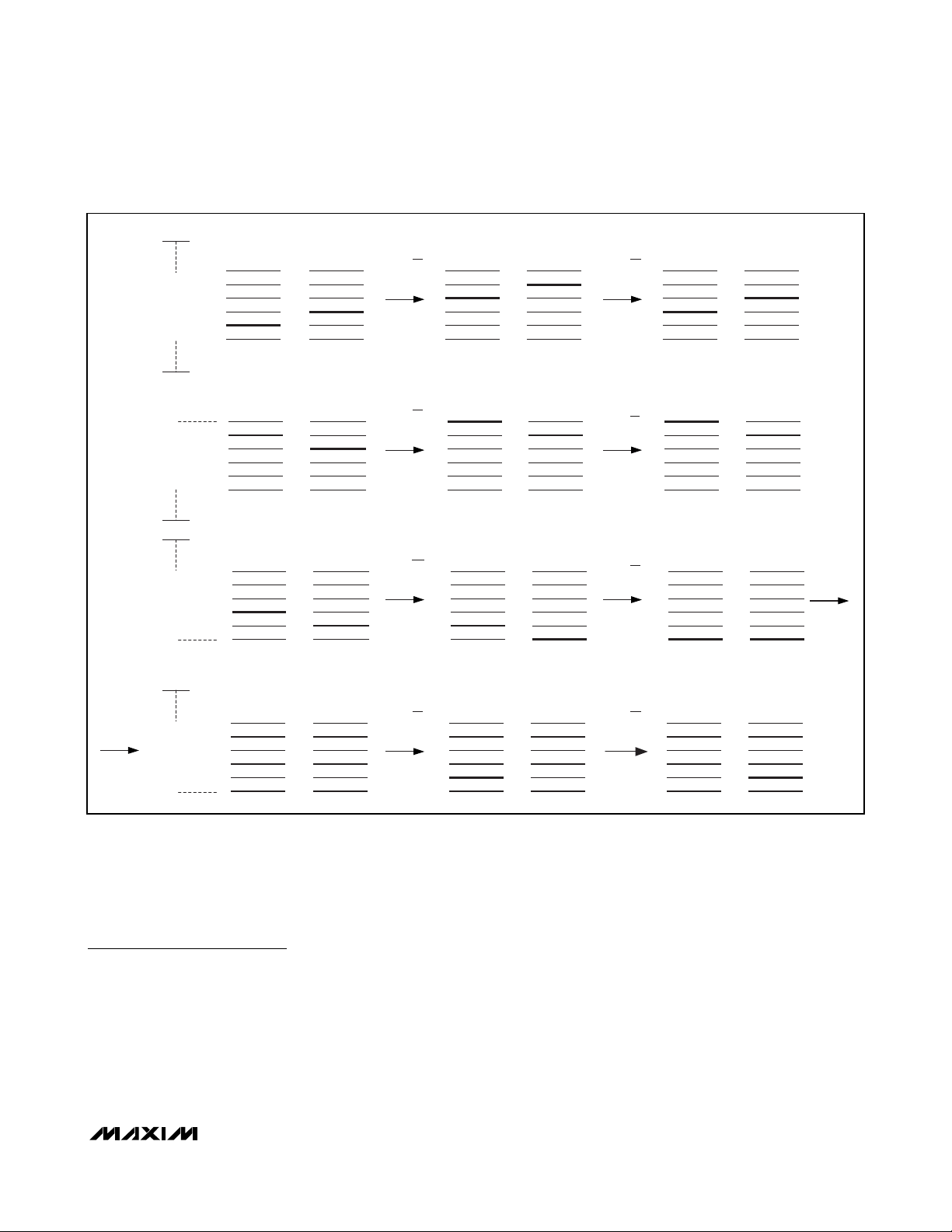
Volume Control
In volume-control mode, the MAX5486’s wipers move
simultaneously, maintaining the balance separation
between each wiper (Figure 2a).
When either wiper reaches the maximum tap position
(position closest to H_), further commands to increase
the volume are ignored. Balance separation is maintained in the maximum volume configuration (Figure 2b).
When either wiper reaches the minimum tap position
(position closest to L_), further commands to decrease
the volume adjust the other wiper until it also reaches
the minimum tap position (Figure 2c). Increasing the
volume from this minimum position restores the original
balance separation of the wipers (Figure 2d).
Figure 1. Pushbutton Interface
Table 1. Wiper Position and Attenuation
Table 2. Wiper Action vs. Pushbutton
Contact Duration
MOMENTARY
CONTACT
SPST
PUSHBUTTONS
POSITION ATTENUATION (dB)
00
12
24
36
48
MM
30 60
31 62
32 (mute) > 90
CONTACT DURATION WIPER ACTION
t ≤ 16ms No motion.
16ms < t ≤ 250ms Wiper changes position once.
250ms < t ≤ 500ms
500ms < t ≤ 1000ms
t > 1000 ms
SmartWiper begins. Wiper
changes position at a rate of 4Hz.
Wiper changes position at a rate
of 8Hz.
Wiper changes position at a rate
of 11Hz.
UP
DN
V
GND
LOGIC
MAX5486
Page 9
MAX5486
Stereo Volume Control with Pushbutton
Interface
_______________________________________________________________________________________ 9
When both wipers are in the tap 31 position (-62dB
attenuation), further commands to DN/BALR place the
wipers in the mute position (see Table 1). UP/BALL or
MUTE pulses return the wipers to tap 31.
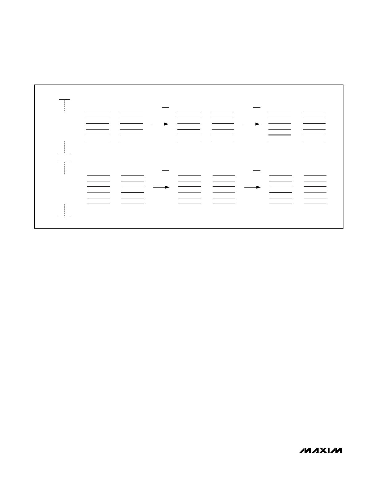
Balance Control
In balance-control mode, the MAX5486 adjusts the balance between the right and left channels while maintaining the set volume. For example, if the volume of the
right channel equals the volume of the left channel,
forcing the balance towards the left channel increases
the attenuation of the right channel (Figure 3a). If the
left channel is at a higher attenuation than the right
channel, adjusting the balance to the left channel
moves the left channel’s wiper up to the same wiper
position as the right channel before it was attenuated
(Figure 3b).
Click-and-Pop Suppression
The click-and-pop suppression feature reduces the
audible noise (clicks and pops) that results from wiper
transitions. The MAX5486 minimizes this noise by allowing the wiper to change position only when VH= V
L
(zero crossing) or after the zero crossing timeout
(126ms). Each wiper has its own suppression and timeout circuitry. The MAX5486 changes wiper position
when VH= VL, or after 32ms, whichever occurs first
(see Figures 4a and 4b).
The suppression circuitry monitors left and right channels separately. In volume-control mode, when the first
_______________________________________________________________________________________ 9
Figures 2a–2d. Volume-Control Operation
BALANCE SEPARATION
H_
WR
(2a)
L_
WR WL
H_
(2b)
L_
H_
WR WL
(2c)
L_
WL
PRESS UP
TWICE
PRESS UP
ONCE
PRESS DN
ONCE
WR
WR
WR
PRESS DN
ONCE
PRESS UP
ONCE
PRESS DN
ONCE
MAINTAINED
WRWL WL
NO CHANGE
WRWL WL
WRWL WL
TO 2d
H_
WR WL
FROM 2c
(2d)
L_
PRESS UP
ONCE
ORIGINAL BALANCE SEPARATION
MAINTAINED
WR
PRESS UP
ONCE
WRWL WL
Page 10
MAX5486
wiper changes position, the second wiper has 126ms
to change or it changes automatically.
Power-On Reset
The power-on comparators monitor (VDD- VSS) and
(V
LOGIC
- GND). A power-on reset is initiated when
either of the supplies is brought back to the normal
operating voltage. The power-on reset feature sets both
wipers to -12dB. The wipers initially wake up in mute
mode (-90dB) and move to the -12dB position when
VH= VLto eliminate clicks and pops during power-up.
With DC inputs at VHand VL, the wipers move after
exceeding the timeout period. A power-on reset places
the MAX5486 in volume-control mode.
Shutdown (
SHDN
)
Upon entering shutdown, the MAX5486 stores the last
wiper settings. The wipers move to the L_ end of the
resistor string when VH= VLto eliminate clicks and
pops during shutdown. With DC inputs at VHand VL,
the wipers move after exceeding the timeout period.
Exiting shutdown restores the wipers to their previous
settings. Shutdown also turns off all the LED indicators
to save power.
Mute Function (
MUTE
)
The MAX5486 features a mute function input, MUTE.
Successive low pulses on MUTE toggle its setting.
Activating the mute function forces both wipers to maximum attenuation (-90dB typ). Deactivating the mute
function returns the wipers to their previous settings.
MUTE is internally pulled high with a resistor to V
LOGIC
.
When both wipers are in the tap 31 position
(-62dB attenuation) further commands to lower the volume place the wipers in the mute position (see Table 1).
Mode Indicator (
MODEIND
)
The open-drain MODEIND indicates volume-control
mode or balance-control mode for the MAX5486.
Connect MODEIND to an LED with a series resistor to
V
LOGIC
. When the LED is on, the MAX5486 is in balance-control mode. When the LED is off, the MAX5486
is in volume-control mode. See the
Mode Control
(MODE)
section for more detail on switching between
modes.
Level Indicator LEDs
The MAX5486 includes five indicator LED drivers to display the current wiper settings in either volume or balance mode. The LED indicators are enabled by
connecting a 1MΩ resistor between LEDIND4 and
V
LOGIC
. Connect the LEDIND_ outputs to the LEDs and
to V
LOGIC
through a series resistor as shown in the
Typical Operating Circuit
. Connect LEDIND_ outputs to
GND when LED indicator drivers are not used.
In volume-control mode, all LEDs are off when the
wipers reach the highest attenuation levels (mute). All
LEDs are on at the lowest attenuation levels (0dB).
Stereo Volume Control with Pushbutton
Interface
10 ______________________________________________________________________________________
Figures 3a and 3b. Balance-Control Operation
H_
(3a)
L_
H_
(3b)
L_
VOLUME LEVEL IS SET
WR
WR WL
WL
PRESS BALL
ONCE
PRESS BALL
ONCE
VOLUME LEVEL MAINTAINED
BALANCE SHIFTS TO WL
WR
WR
PRESS BALL
ONCE
PRESS BALL
ONCE
WRWL WL
VOLUME LEVEL MAINTAINED
BALANCE SHIFTS TO WLVOLUME LEVEL IS SET BY WR
WRWL WL
Page 11
Table 3 shows the LED display as the wipers transition
through various attenuation levels.
A PWM circuit interpolates the high-resolution 32 steps
between the five LEDs over the volume range from 0dB
to -54dB. This feature provides visible indication for the
attenuation levels from 0dB to -54dB. For example,
LED4 brightness level decreases progressively with
each -2dB step from 0dB to -8dB. PWM is disabled in
the range -56dB to mute.
In balance-control mode, only one LED is on at a time
to indicate the current balance setting. Figure 5 shows
the LEDs display for the current balance setting. When
LED2 is on, the display indicates that the channels are
centered or balanced at a set volume level. When LED4
turns on, the balance shifts completely toward the right
channel and the left channel becomes fully attenuated.
Multiple Button Pushes
The MAX5486 does not respond to simultaneous button
pushes. Additionally, a 16ms blocking period affects all
other inputs when releasing any input that was forced low.
The MAX5486 does not respond to any logic input until
the blocking period ends. If multiple-control buttons are
pressed, all wiper-control connections must be released
before the device responds to further commands.
Applications Information
The
Typical Operating Circuit
shows a typical volume/
balance application circuit using the MAX5486 in a single-supply configuration. The internally generated BIAS
voltage eliminates the need for external op amps, and
the wipers have internal low-power buffers for low distortion. Connect the W_ outputs of the MAX5486 to the
left and right inputs of a stereo audio amplifier, such as
the MAX9761. The pushbutton potentiometers attenuate the input signals. Use the MODE input to switch
between volume-control and balance-control modes.
MAX5486
Stereo Volume Control with Pushbutton
Interface
______________________________________________________________________________________ 11
Table 3. LED Settings in Volume Mode
VOLUME POSITION
0dB to -8dB 11111
-10dB to -18dB 11110
-20dB to -28dB 11100
-30dB to -38dB 11000
-40dB to -52dB 10000
-54dB to mute (-90dB) 00000
LED0 LED1 LED2 LED3 LED4
VOLUME LED OUTPUTS ( 1 = LED IS ON)
Page 12

MAX5486
Stereo Volume Control with Pushbutton
Interface
12 ______________________________________________________________________________________
Figure 4a. Wiper Transition Timing Diagram—Suppression Circuitry Active
DN OR UP
USER PRESSES PUSHBUTTON
1
0
IS BOUNCING
V
H
V
L
SWITCH
CONTACT
SWITCH
CONTACT
IS STABLE
t
IPW
DEBOUNCE BY
WAITING FOR
STABLE LOW, t
CROSSING, t
IPW
WAIT FOR
FIRST ZERO
INPUT ACCEPTED
t
WS
WS
SWITCH
CONTACT
IS BOUNCING
DEBOUNCE BY
STABLE HIGH, t
t
HPW
WAITING FOR
HPW
READY TO ACCEPT
ANOTHER KEYPRESS
WIPER MOVES HERE
WIPER MOTION
2dB
STEPS
Page 13

MAX5486
Stereo Volume Control with Pushbutton
Interface
______________________________________________________________________________________ 13
Figure 4b. Wiper Transition Timing Diagram—Timeout
Figure 5. LED Settings in Balance Mode
SWITCH
CONTACT
IS BOUNCING
1
0
V
H
V
L
SWITCH
CONTACT
IS STABLE
t
IPW
DEBOUNCE BY
WAITING FOR
STABLE LOW,
t
IPW
INPUT ACCEPTED
t
WS
WAIT FOR
FIRST ZERO
CROSSING OR
TIMEOUT, t
WS
SWITCH
CONTACT
IS BOUNCING
STABLE HIGH, t
t
HPW
DEBOUNCE BY
WAITING FOR
HPW
READY TO ACCEPT
ANOTHER KEYPRESS
(t
IPW
FULL L
LED0 ON LED1 ON LED2 ON LED3 ON LED4 ON
L + 12 L + 6 R + 6 R + 12 FULL R
+ tWS)
CENTERED
WIPER MOVES HERE
2dB
STEPS
PB PRESS (CHANNEL R) PB PRESS (CHANNEL L)
Page 14

MAX5486
Stereo Volume Control with Pushbutton
Interface
14 ______________________________________________________________________________________
Functional Diagram
V
DD
V
HR
MAX5486
DD
BIAS GENERATOR
V
SS
BIAS
BIASCAP
WR
LR
MODE
LED DRIVERS
GND
V
SS
SHDNMUTE
HL
SWITCH CONTROL, CLICK-AND-POP SUPPRESSION
LL
DEBOUNCE, TIMEOUT, ACCELERATION
UP/BALL DN/BALR
WL
MODEIND
LEDIND4
LEDIND3
LEDIND2
LEDIND1
LEDIND0
V
LOGIC
Page 15

MAX5486
Stereo Volume Control with Pushbutton
Interface
______________________________________________________________________________________ 15
Pin Configuration
Chip Information
PROCESS: BiCMOS
TOP VIEW
V
LOGIC
DN/BALR
UP/BALL
MODE
SHDN
N.C.
WR
BIAS
BIASCAP
+
1
2
3
4
MAX5486
5
6
7
8
9
LR
10
11
12
TSSOP
24
23
22
21
20
19
18
17
16
15
14
13
GND
MODEIND
LEDIND4
LEDIND3MUTE
LEDIND2
LEDIND1
LEDIND0
HLHR
LL
WL
V
SS
V
DD
Page 16

MAX5486
Stereo Volume Control with Pushbutton
Interface
Maxim cannot assume responsibility for use of any circuitry other than circuitry entirely embodied in a Maxim product. No circuit patent licenses are
implied. Maxim reserves the right to change the circuitry and specifications without notice at any time.
16
____________________Maxim Integrated Products, 120 San Gabriel Drive, Sunnyvale, CA 94086 408-737-7600
© 2006 Maxim Integrated Products is a registered trademark of Maxim Integrated Products. Inc.
Package Information
(The package drawing(s) in this data sheet may not reflect the most current specifications. For the latest package outline information
go to www.maxim-ic.com/packages
.)
PACKAGE OUTLINE, TSSOP 4.40mm BODY
21-0066
G
TSSOP4.40mm.EPS
1
1
 Loading...