

Page 1
General Description
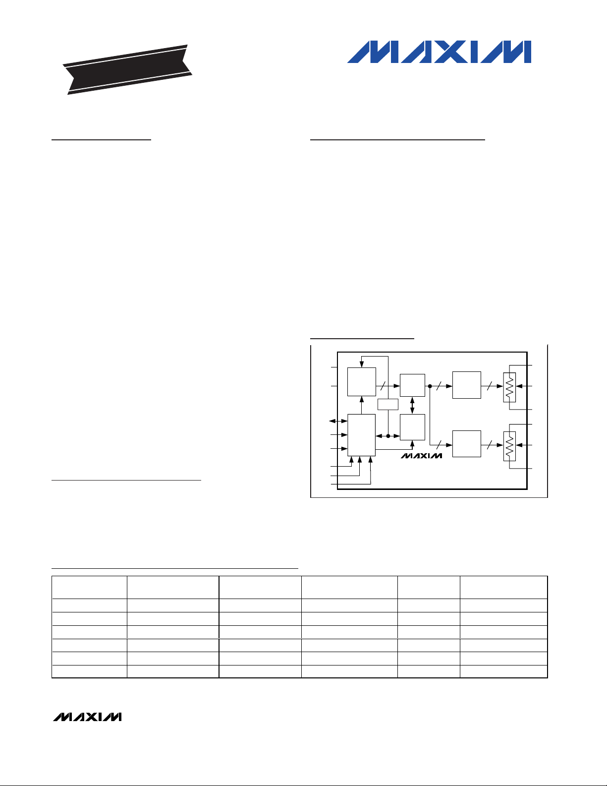
The MAX5477/MAX5478/MAX5479 nonvolatile, dual,
linear-taper, digital potentiometers perform the function
of a mechanical potentiometer, but replace the
mechanics with a simple 2-wire digital interface. Each
device performs the same function as a discrete potentiometer or variable resistor and has 256 tap points.
The devices feature an internal, nonvolatile EEPROM
used to store the wiper position for initialization during
power-up. A write-protect feature prevents accidental
overwrites of the EEPROM. The fast-mode I2C-compatible serial interface allows communication at data rates
up to 400kbps, minimizing board space and reducing
interconnection complexity in many applications. Three
address inputs allow a total of eight unique address
combinations.
The MAX5477/MAX5478/MAX5479 provide three nominal resistance values: 10kΩ (MAX5477), 50kΩ
(MAX5478), or 100kΩ (MAX5479). The nominal resistor
temperature coefficient is 70ppm/°C end-to-end and
10ppm/°C ratiometric. The low temperature coefficient
makes the devices ideal for applications requiring a lowtemperature-coefficient variable resistor, such as lowdrift, programmable gain-amplifier circuit configurations.
The MAX5477/MAX5478/MAX5479 are available in 16pin 3mm x 3mm x 0.8mm thin QFN and 14-pin 4.4mm x
5mm TSSOP packages. These devices operate over
the extended -40°C to +85°C temperature range.
Applications
Mechanical Potentiometer Replacement
Low-Drift Programmable-Gain Amplifiers
Volume Control
Liquid-Crystal Display (LCD) Contrast Control
Features
♦ Power-On Recall of Wiper Position from
Nonvolatile Memory
♦ EEPROM Write Protection
♦ Tiny 3mm x 3mm x 0.8mm Thin QFN Package
♦ 70ppm/°C End-to-End Resistance Temperature
Coefficient
♦ 10ppm/°C Ratiometric Temperature Coefficient
♦ Fast 400kbps I2C-Compatible Serial Interface
♦ 1µA (max) Static Supply Current
♦ Single-Supply Operation: +2.7V to +5.25V
♦ 256 Tap Positions per Potentiometer
♦ ±0.5 LSB DNL in Voltage-Divider Mode
♦ ±1 LSB INL in Voltage-Divider Mode
MAX5477/MAX5478/MAX5479
Dual, 256-Tap, Nonvolatile,
I2C-Interface, Digital Potentiometers
________________________________________________________________ Maxim Integrated Products 1
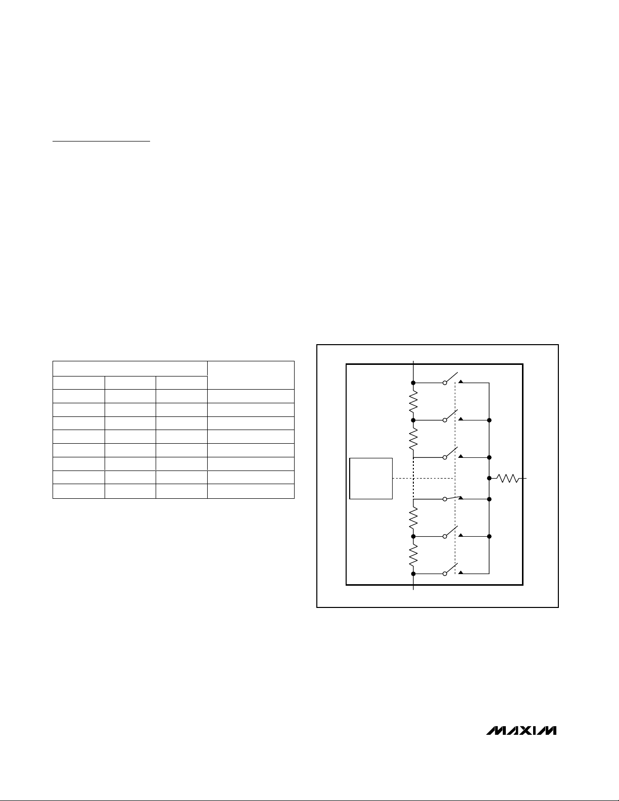
MAX5477
MAX5478
MAX5479
8-BIT
SHIFT
REGISTER
POR
16-BIT
LATCH
16-BIT
NV
MEMORY
SDA
SCL
WP
A0
A1
A2
8
256
POSITION
DECODER
8
8
256
256
POSITION
DECODER
256
HA
WA
LA
HB
WB
LB
V
DD
GND
I2C
INTERFACE
Functional Diagram
19-3379; Rev 4; 1/06
For pricing, delivery, and ordering information, please contact Maxim/Dallas Direct! at
1-888-629-4642, or visit Maxim’s website at www.maxim-ic.com.
Pin Configurations appear at end of data sheet.
Purchase of I2C components from Maxim Integrated Products,
Inc. or one of its sublicensed Associated Companies, conveys
a license under the Philips I
2
C Patent Rights to use these com-
ponents in an I
2
C system, provided that the system conforms
to the I
2
C Standard Specification as defined by Philips.
EVALUATION KIT
AVAILABLE
Ordering Information/Selector Guide
PART TEMP RANGE PIN-PACKAGE
END-TO-END
RESISTANCE (kΩ)
TOP
MARK
PACKAGE CODE
MAX5477ETE* -40°C to +85°C 16 Thin QFN 10 ABO T1633F-3
MAX5477EUD -40°C to +85°C 14 TSSOP 10 — U14-1
MAX5478ETE* -40°C to +85°C 16 Thin QFN 50 ABP T1633F-3
MAX5478EUD -40°C to +85°C 14 TSSOP 50 — U14-1
MAX5479ETE* -40°C to +85°C 16 Thin QFN 100 ABQ T1633F-3
MAX5479EUD -40°C to +85°C 14 TSSOP 100 — U14-1
*Future product—contact factory for availability.
Page 2
MAX5477/MAX5478/MAX5479
Dual, 256-Tap, Nonvolatile, I2C-Interface,
Digital Potentiometers
2 _______________________________________________________________________________________
ABSOLUTE MAXIMUM RATINGS
ELECTRICAL CHARACTERISTICS
(VDD= +2.7V to +5.25V, H_ = VDD, L_ = GND, TA= -40°C to +85°C, unless otherwise noted. Typical values are at VDD= +5V, TA=
+25°C.) (Note 1)
Stresses beyond those listed under “Absolute Maximum Ratings” may cause permanent damage to the device. These are stress ratings only, and functional
operation of the device at these or any other conditions beyond those indicated in the operational sections of the specifications is not implied. Exposure to
absolute maximum rating conditions for extended periods may affect device reliability.
SDA, SCL, VDDto GND.........................................-0.3V to +6.0V
All Other Pins to GND.................................-0.3V to (V
DD
+ 0.3V)
Maximum Continuous Current into H_, L_, and W_
MAX5477......................................................................
±5.0mA
MAX5478......................................................................±1.3mA
MAX5479......................................................................±0.6mA
Continuous Power Dissipation (T
A
= +70°C)
16-Pin Thin QFN (derate 17.5mW/°C above +70°C) 1398mW
14-Pin TSSOP (derate 9.1mW/°C above +70°C) .........727mW
Operating Temperature Range ...........................-40°C to +85°C
Maximum Junction Temperature .....................................+150°C
Storage Temperature Range .............................-65°C to +150°C
Lead Temperature (soldering, 10s) .................................+300°C
PARAMETER
SYMBOL
CONDITIONS MIN TYP MAX
UNITS
DC PERFORMANCE (VOLTAGE-DIVIDER MODE)
Resolution 256
Taps
Integral Nonlinearity INL (Note 2) ±1 LSB
Differential Nonlinearity DNL (Note 2) ±0.5 LSB
Dual Code Matching
±1 LSB
End-to-End Resistance
Temperature Coefficient
TC
R
70
ppm/°C
Ratiometric Resistance
Temperature Coefficient
10
ppm/°C
MAX5477 -4
MAX5478 -0.6
Full-Scale Error
MAX5479 -0.3
LSB
MAX5477 4
MAX5478 0.6Zero-Scale Error
MAX5479 0.3
LSB
DC PERFORMANCE (VARIABLE-RESISTOR MODE)
V
DD
= 3V ±3
Integral Nonlinearity (Note 3) INL
V
DD
= 5V ±1.5
LSB
MAX5477 ±1
MAX5478 ±1
Differential Nonlinearity (Note 3) DNL
MAX5479 ±1
LSB
Dual Code Matching
R0 and R1 set to same code
(all codes), V
DD
= 3V or 5V
±3 LSB
DC PERFORMANCE (RESISTOR CHARACTERISTICS)
Wiper Resistance R
W
(Note 4) 325 675 Ω
Wiper Capacitance C
W
10 pF
MAX5477 7.5 10 12.5
MAX5478 37.5 50 62.5
End-to-End Resistance R
HL
MAX5479 75 100 125
kΩ
R0 and R1 set to same code (all codes)
Page 3
MAX5477/MAX5478/MAX5479
Dual, 256-Tap, Nonvolatile, I2C-Interface,
Digital Potentiometers
_______________________________________________________________________________________ 3
ELECTRICAL CHARACTERISTICS (continued)
(VDD= +2.7V to +5.25V, H_ = VDD, L_ = GND, TA= -40°C to +85°C, unless otherwise noted. Typical values are at VDD= +5V, TA=
+25°C.) (Note 1)
PARAMETER
SYMBOL
CONDITIONS MIN TYP MAX
UNITS
DIGITAL INPUTS
VDD = 3.4V to 5.25V 2.4
Input High Voltage (Note 5) V
IH
VDD < 3.4V
V
Input Low Voltage V
IL
(Note 5) 0.8 V
Output Low Voltage V
OL
I
SINK
= 3mA 0.4 V
WP Pullup Resistance I
WP
255 kΩ
Input Leakage Current I
LEAK
±1 µA
Input Capacitance 5pF
DYNAMIC CHARACTERISTICS
Crosstalk
HA = 1kHz (0 to V
DD
), LA = GND,
LB = GND, measure WB
-75 dB
MAX5477 400
MAX5478 100
3dB Bandwidth (Note 6)
MAX5479 50
kHz
Total Harmonic Distortion Plus
Noise
H_ = 1V
RMS
, f = 1kHz, L_ = GND,
measure W_
%
NONVOLATILE MEMORY RELIABILITY
Data Retention TA = +85°C 50
Years
TA = +25°C
Endurance
T
A
= +85°C
Stores
POWER SUPPLY
Power-Supply Voltage V
DD
2.70 5.25 V
Writing to EEPROM, digital inputs at
GND or V
DD
, TA = +25°C (Note 7)
250 400
15 20.6
Supply Current I
DD
Normal operation, digital
inputs at GND or V
DD
,
T
A
= +25°C
WP = V
DD
0.5 1
µA
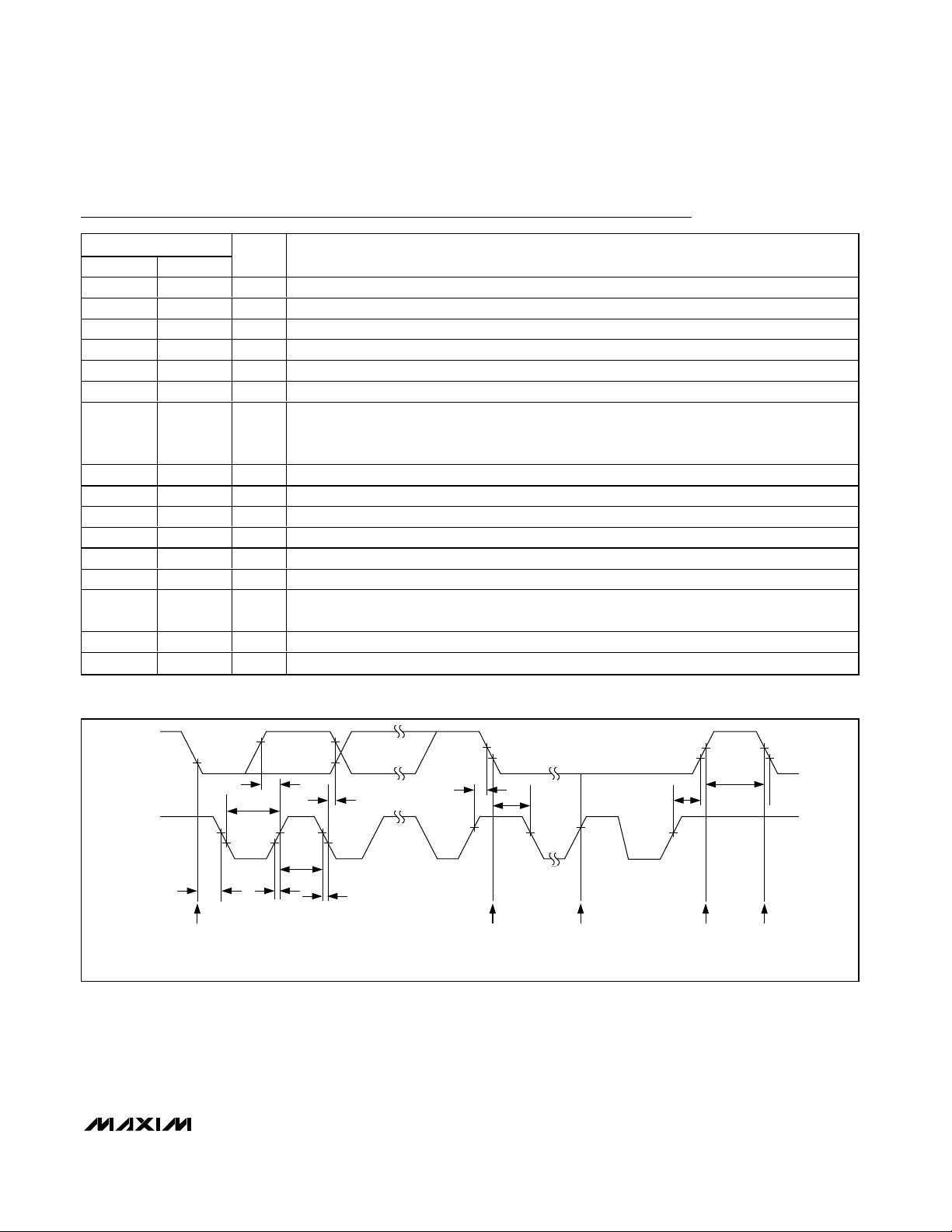
TIMING CHARACTERISTICS
(VDD= +2.7V to +5.25V, H_ = VDD, L_ = GND, TA= -40°C to +85°C, unless otherwise noted. Typical values are at VDD= +5V,
T
A
= +25°C. See Figure 1.) (Notes 8 and 9)
0.7 x V
DD
THD+N
ANALOG SECTION
DIGITAL SECTION
SCL Clock Frequency f
Setup Time for START Condition t
Hold Time for START Condition t
PARAMETER SYMBOL CONDITIONS MIN TYP MAX UNITS
SU:STA
HD:STA
WP = GND
MAX5477 325
WS
SCL
MAX5478 500Wiper Settling Time (Note 10) t
MAX5479 1000
0.003
200,000
50,000
400 kHz
0.6 µs
0.6 µs
ns
Page 4
MAX5477/MAX5478/MAX5479
Dual, 256-Tap, Nonvolatile, I2C-Interface,
Digital Potentiometers
4 _______________________________________________________________________________________
Note 1: All devices are production tested at TA= +25°C and are guaranteed by design and characterization for -40°C < TA< +85°C.
Note 2: The DNL and INL are measured with the potentiometer configured as a voltage-divider with H_ = V
DD
and L_ = GND. The
wiper terminal is unloaded and measured with a high-input-impedance voltmeter.
Note 3: The DNL and INL are measured with the potentiometer configured as a variable resistor. H_ is unconnected and L_ =
GND. For V
DD
= +5V, the wiper is driven with 400µA (MAX5477), 80µA (MAX5478), or 40µA (MAX5479). For VDD= +3V,
the wiper is driven with 200µA (MAX5477), 40µA (MAX5478), or 20µA (MAX5479).
Note 4: The wiper resistance is measured using the source currents given in Note 3.
Note 5: The devices draw current in excess of the specified supply current when the digital inputs are driven with voltages between
(V
DD
- 0.5V) and (GND + 0.5V). See Supply Current vs. Digital Input Voltage in the Typical Operating Characteristics.
Note 6: Wiper at midscale with a 10pF load (DC measurement). L_ = GND, an AC source is applied to H_, and the W_ output is
measured. A 3dB bandwidth occurs when the AC W_/H_ value is 3dB lower than the DC W_/H_ value.
Note 7: The programming current exists only during power-up and EEPROM writes.
Note 8: The SCL clock period includes rise and fall times (t
R
= tF). All digital input signals are specified with tR= tF= 2ns and
timed from a voltage level of (V
IL
+ VIH) / 2.
Note 9: Digital timing is guaranteed by design and characterization, and is not production tested.
Note 10: This is measured from the STOP pulse to the time it takes the output to reach 50% of the output step size (divider mode). It
is measured with a maximum external capacitive load of 10pF.
Note 11: An appropriate bus pullup resistance must be selected depending on board capacitance. Refer to the I
2
C-bus specifica-
tion document linked to this web address: www.semiconductors.philips.com/acrobat/literature/9398/39340011.pdf
Note 12: The idle time begins from the initiation of the STOP pulse.
PARAMETER
CONDITIONS
UNITS
SCL High Time t
HIGH
0.6 µs
SCL Low Time t
LOW
1.3 µs
Data Setup Time
100 ns
Data Hold Time
0 0.9 µs
SDA, SCL Rise Time t
R
300 ns
SDA, SCL Fall Time t
F
300 ns
Setup Time for STOP Condition
0.6 µs
Bus Free Time Between STOP
and START Condition
t
BUF
Minimum power-up rate = 0.2V/µs 1.3 µs
Pulse Width of Spike Suppressed
t
SP
50 ns
Capacitive Load for Each Bus
Line
C
B
(Note 11) 400 pF
Write NV Register Busy Time (Note 12) 12 ms
TIMING CHARACTERISTICS (continued)
(VDD= +2.7V to +5.25V, H_ = VDD, L_ = GND, TA= -40°C to +85°C, unless otherwise noted. Typical values are at VDD= +5V,
T
A
= +25°C. See Figure 1.) (Notes 8 and 9)
SYMBOL
t
SU:DAT
t
HD:DAT
t
SU:STO
MIN TYP MAX
Page 5
MAX5477/MAX5478/MAX5479
Dual, 256-Tap, Nonvolatile, I2C-Interface,
Digital Potentiometers
_______________________________________________________________________________________ 5
0
0.2
0.6
0.4
0.8
1.0
-40 10-15 35 60 85
SUPPLY CURRENT
vs. TEMPERATURE (MAX5477)
MAX5477/78/79 toc01
TEMPERATURE (°C)
SUPPLY CURRENT (µA)
VCC = 5V
WP = V
DD
VCC = 3V
5
7
11
9
13
15
-40 10-15 35 60 85
SUPPLY CURRENT
vs. TEMPERATURE
MAX5477/78/79 toc1a
TEMPERATURE (°C)
SUPPLY CURRENT (µA)
VCC = 5V
WP = GND
VCC = 3V
0
100
50
200
150
300
250
350
450
400
500
0649632 128 160 192 224 256
WIPER RESISTANCE
vs. INPUT CODE
MAX5477/78/79 toc02
INPUT CODE
WIPER RESISTANCE (Ω)
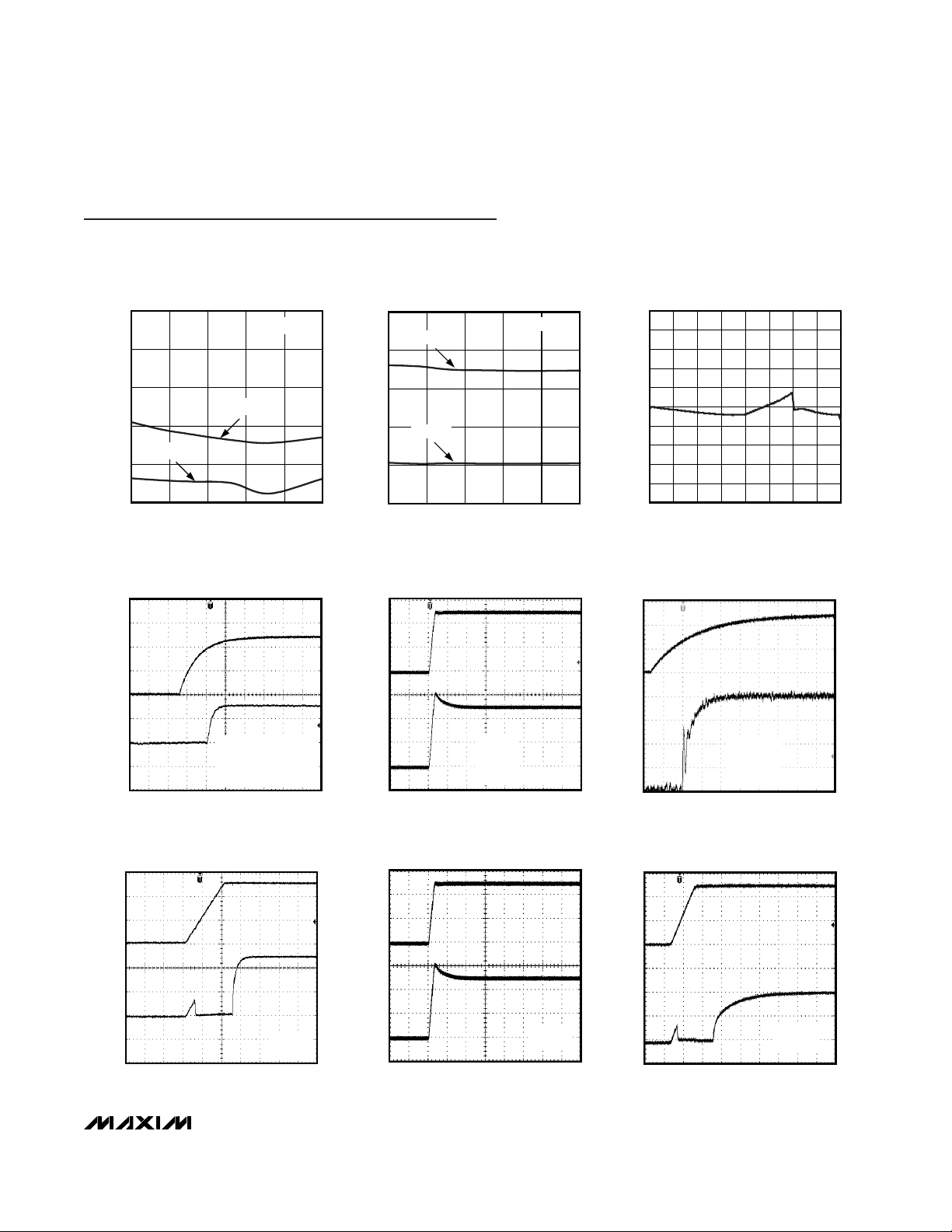
200ns/div
TAP-TO-TAP SWITCHING TRANSIENT
SDA
2V/div
W_
50mV/div
MAX5477/78/79 toc03
MAX5477
C
L
= 10pF
H_ = V
DD
FROM TAP 00 TO TAP 04
TAP-TO-TAP SWITCHING TRANSIENT
MAX5477/78/79 toc04
1µs/div
SDA
2V/div
W_
20mV/div
MAX5478
C
L
= 10pF
H_ = V
DD
FROM TAP 00 TO TAP 04
TAP-TO-TAP SWITCHING TRANSIENT
MAX5477/78/79 toc05
400ns/div
SDA
2V/div
W_
20mV/div
MAX5479
C
W_
= 10pF
H_ = V
DD
FROM TAP 00 TO TAP 04
2µs/div
WIPER TRANSIENT AT POWER-ON
V
DD
2V/div
W_
1V/div
MAX5477/78/79 toc06
MAX5477
TAP = 128
WIPER TRANSIENT AT POWER-ON
MAX5477/78/79 toc07
4µs/div
V
DD
2V/div
W_
1V/div
MAX5478
TAP = 128
WIPER TRANSIENT AT POWER-ON
MAX5477/78/79 toc08
2µs/div
V
DD
2V/div
W_
1V/div
MAX5479
TAP = 128
Typical Operating Characteristics
(VDD= +5V, H_ = VDD, L_ = GND, TA= +25°C, unless otherwise noted.)
Page 6
MAX5477/MAX5478/MAX5479
Dual, 256-Tap, Nonvolatile, I2C-Interface,
Digital Potentiometers
6 _______________________________________________________________________________________
-0.3
-0.2
-0.1
0
0.1
0.2
0.3
06432 96 128 160 192 224 256
DIFFERENTIAL NONLINEARITY
vs. CODE (VDM MODE)
MAX5477/78/79 toc10
CODE
DNL (LSB)
MAX5477
-0.3
-0.2
-0.1
0
0.1
0.2
0.3
06432 96 128 160 192 224 256
INTEGRAL NONLINEARITY
vs. CODE (VDM MODE)
MAX5477/78/79 toc11
CODE
INL (LSB)
MAX5478
-0.3
-0.2
-0.1
0
0.1
0.2
0.3
06432 96 128 160 192 224 256
DIFFERENTIAL NONLINEARITY
vs. CODE (VDM MODE)
MAX5477/78/79 toc12
CODE
DNL (LSB)
MAX5478
-0.3
-0.2
-0.1
0
0.1
0.2
0.3
06432 96 128 160 192 224 256
INTEGRAL NONLINEARITY
vs. CODE (VRM MODE)
MAX5477/78/79 toc13
CODE
INL (LSB)
MAX5478
-0.10
-0.08
-0.04
0
0.02
0.06
0.10
06432 96 128 160 192 224 256
DIFFERENTIAL NONLINEARITY
vs. CODE (VRM MODE)
MAX5477/78/79 toc14
CODE
DNL (LSB)
-0.06
-0.02
0.08
0.04
MAX5478
-0.20
-0.12
-0.16
-0.04
-0.08
0.04
0
0.08
0.16
0.12
0.20
0649632 128 160 192 224 256
INTEGRAL NONLINEARITY
vs. CODE (VDM MODE)
MAX5477/78/79 toc15
CODE
INL (LSB)
MAX5479
-0.14
-0.02
-0.04
-0.06
-0.08
-0.10
-0.12
0
0.04
0.02
0.10
0.08
0.12
0.06
0.14
06432 96 128 160 192 224 256
DIFFERENTIAL NONLINEARITY
vs. CODE (VDM MODE)
MAX5477/78/79 toc16
CODE
DNL (LSB)
MAX5479
-0.20
-0.12
-0.16
-0.04
-0.08
0.04
0
0.08
0.16
0.12
0.20
0649632 128 160 192 224 256
INTEGRAL NONLINEARITY
vs. CODE (VRM MODE)
MAX5477/78/79 toc17
CODE
INL (LSB)
MAX5479
Typical Operating Characteristics (continued)
(VDD= +5V, H_ = VDD, L_ = GND, TA= +25°C, unless otherwise noted.)
0
0.05
0.15
0.10
0.25
0.30
0.20
0.35
0649632 128 160 192 224 256
INTEGRAL NONLINEARITY
vs. CODE (VDM MODE)
MAX5477/78/79 toc09
CODE
INL (LSB)
MAX5477
Page 7

MAX5477/MAX5478/MAX5479
Dual, 256-Tap, Nonvolatile, I2C-Interface,
Digital Potentiometers
_______________________________________________________________________________________ 7
-0.20
-0.12
-0.16
-0.04
-0.08
0.04
0
0.08
0.16
0.12
0.20
0649632 128 160 192 224 256
DIFFERENTIAL NONLINEARITY
vs. CODE (VRM MODE)
MAX5477/78/79 toc18
CODE
DNL (LSB)
MAX5479
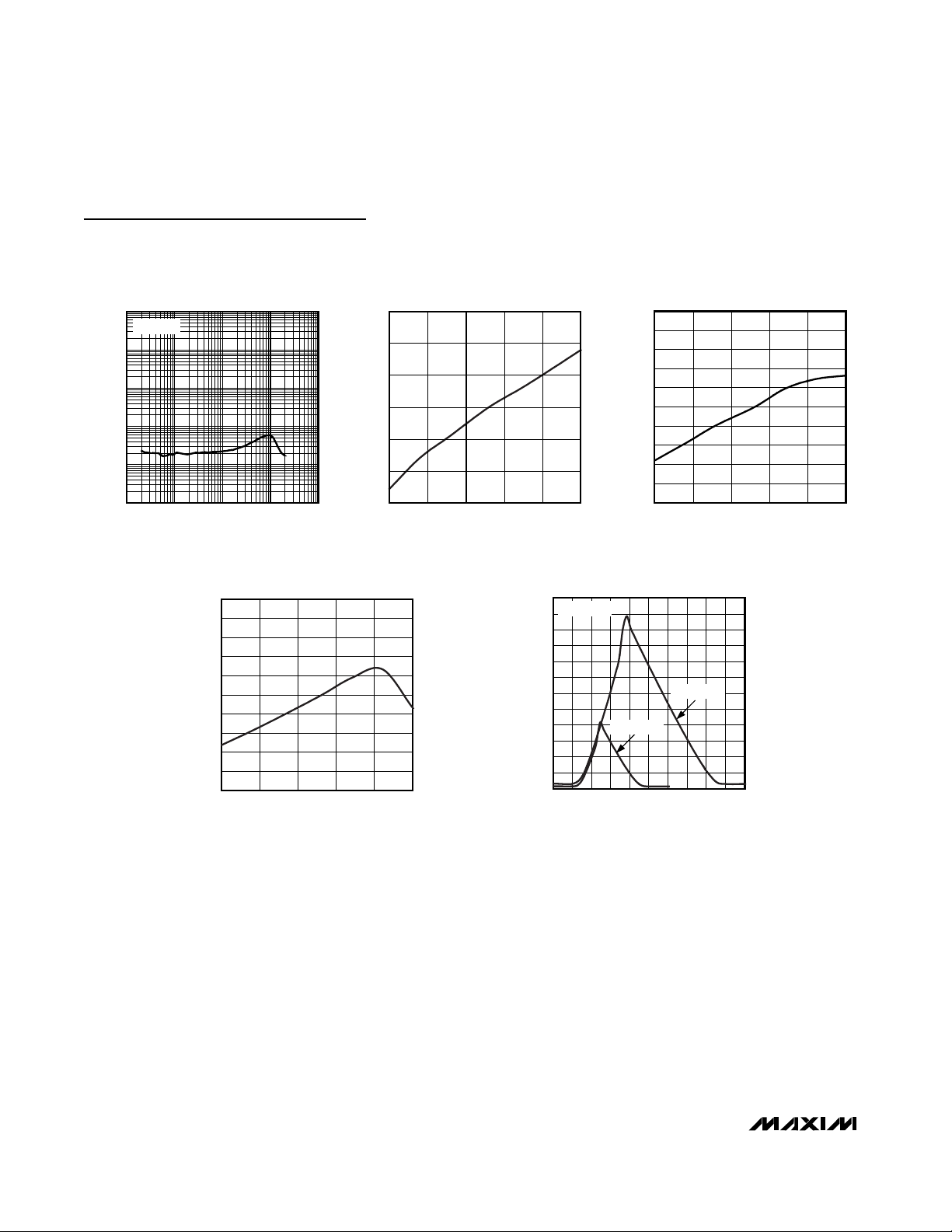
FREQUENCY (kHz)
CROSSTALK (dB)
CROSSTALK vs.
FREQUENCY (MAX5477)
0
-10
-20
-30
-40
-50
-60
-70
-80
-90
-100
0.1 1 10 100 1000 10,000
MAX5477/78/79 toc19
CW_ = 10pF
CROSSTALK vs.
FREQUENCY (MAX5478)
MAX5477/78/79 toc20
FREQUENCY (kHz)
CROSSTALK (dB)
1001010.1
-90
-80
-70
-60
-50
-40
-30
-20
-10
0
-100
0.01 1000
CW_ = 10pF
CROSSTALK vs.
FREQUENCY (MAX5479)
MAX5477/78/79 toc21
FREQUENCY (kHz)
CROSSTALK (dB)
1000100101
-90
-80
-70
-60
-50
-40
-30
-20
-10
0
-100
0.1 10,000
CW_ = 10pF
FREQUENCY (kHz)
GAIN (dB)
MIDSCALE WIPER RESPONSE
vs. FREQUENCY (MAX5477)
1
0
-1
-2
-3
-4
-5
-6
-7
-8
10.1 10 100 1000
MAX5477/78/79 toc22
CW_ = 10pF
C
W_
= 50pF
MIDSCALE WIPER RESPONSE
vs. FREQUENCY (MAX5478)
MAX5477 toc23
FREQUENCY (kHz)
GAIN (dB)
100101
-7
-6
-5
-4
-3
-2
-1
0
1
2
-8
0.1 1000
CW_ = 50pF
C
W_
= 10pF
MIDSCALE WIPER RESPONSE
vs. FREQUENCY (MAX5479)
MAX5477/78/79 toc24
FREQUENCY (kHz)
GAIN (dB)
100101
-4
-3
-2
-1
0
1
2
-5
0.1 1000
CW_ = 50pF
C
W_
= 10pF
FREQUENCY (kHz)
THD+N (%)
TOTAL HARMONIC DISTORTION PLUS NOISE
vs. FREQUENCY (MAX5477)
1
0.1
0.01
0.001
0.01 0.1 1 10 100
MAX5477/78/79 toc25
MIDSCALE
TOTAL HARMONIC DISTORTION PLUS NOISE
vs. FREQUENCY (MAX5478)
MAX5477/78/79 toc26
FREQUENCY (kHz)
THD+N (%)
1010.1
0.001
0.01
0.1
1
10
0.0001
0.01 100
MIDSCALE
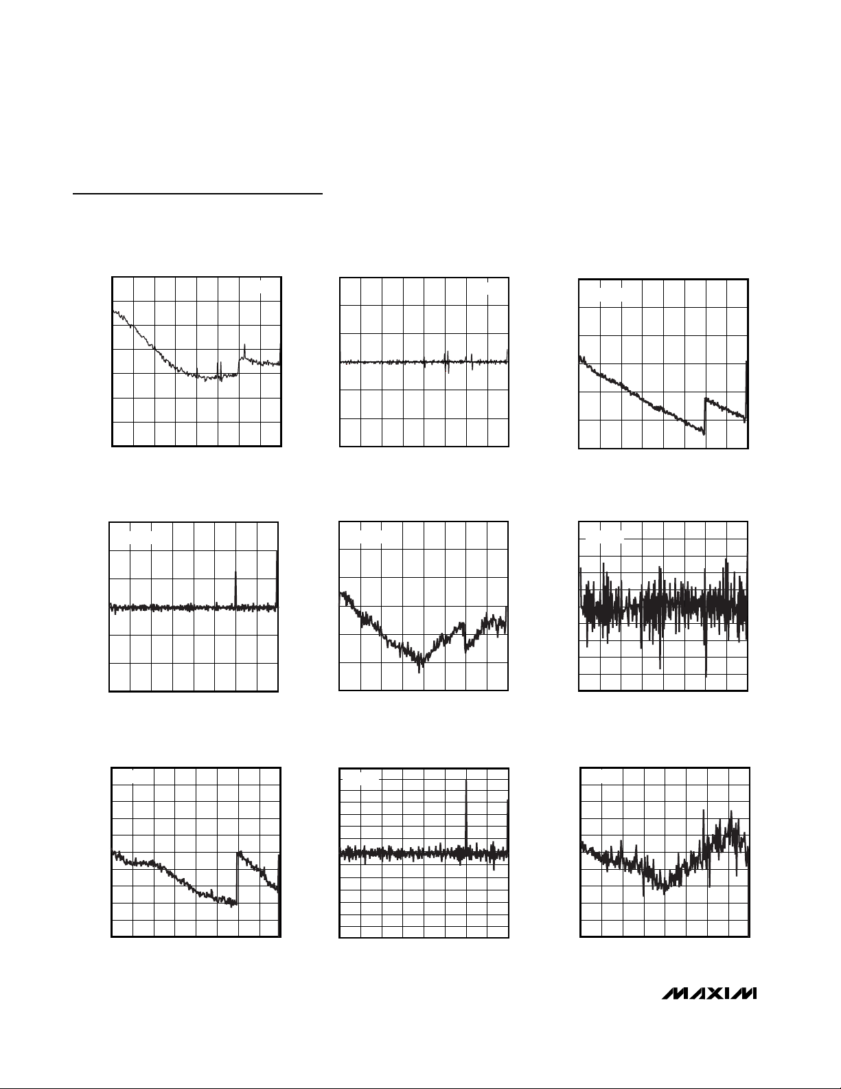
Typical Operating Characteristics (continued)
(VDD= +5V, H_ = VDD, L_ = GND, TA= +25°C, unless otherwise noted.)
Page 8
MAX5477/MAX5478/MAX5479
Dual, 256-Tap, Nonvolatile, I2C-Interface,
Digital Potentiometers
8 _______________________________________________________________________________________
Typical Operating Characteristics (continued)
(VDD= +5V, H_ = VDD, L_ = GND, TA= +25°C, unless otherwise noted.)
TOTAL HARMONIC DISTORTION PLUS NOISE
vs. FREQUENCY (MAX5479)
MAX5477/78/79 toc27
FREQUENCY (kHz)
THD+N (%)
1010.1
0.001
0.01
0.1
1
10
0.0001
0.01 100
MIDSCALE
-0.6
-0.2
-0.4
0.2
0
0.4
0.6
-40 85
END-TO-END RESISTANCE % CHANGE
vs. TEMPERATURE (MAX5477)
MAX5477/78/79 toc28
TEMPERATURE (°C)
END-TO-END RESISTANCE CHANGE (%)
10-15 35 60
-0.5
-0.2
-0.3
-0.4
-0.1
0
0.1
0.2
0.3
0.4
0.5
-40 10-15 35 60 85
END-TO-END RESISTANCE % CHANGE
vs. TEMPERATURE (MAX5478)
MAX5477/78/79 toc29
TEMPERATURE (°C)
END-TO-END RESISTANCE CHANGE (%)
-0.5
-0.2
-0.3
-0.4
-0.1
0
0.1
0.2
0.3
0.4
0.5
-40 10-15 35 60 85
END-TO-END RESISTANCE % CHANGE
vs. TEMPERATURE (MAX5479)
MAX5477/78/79 toc30
TEMPERATURE (°C)
END-TO-END RESISTANCE CHANGE (%)
0
350
300
250
400
450
550
500
600
0 1.00.5 1.5 2.0 2.5 3.0 3.5 4.0 4.5 5.0
SUPPLY CURRENT
vs. DIGITAL INPUT VOLTAGE
MAX5477/78/79 toc31
DIGITAL INPUT VOLTAGE (V)
SUPPLY CURRENT (µA)
WP = GND
VCC = 5V
VCC = 3V
200
150
100
50
Page 9
MAX5477/MAX5478/MAX5479
Dual, 256-Tap, Nonvolatile, I2C-Interface,
Digital Potentiometers
_______________________________________________________________________________________ 9
Pin Description
PIN
TSSOP
FUNCTION
115HAPotentiometer A High Terminal
214WAPotentiometer A Wiper Terminal
313LAPotentiometer A Low Terminal
412HBPotentiometer B High Terminal
511WBPotentiometer B Wiper Terminal
610LBPotentiometer B Low Terminal
79WP
Write-Protect Input. Connect to GND to allow changes to the wiper position and the data stored
in the EEPROM. Connect to V
DD
or leave unconnected to enable the write protection of the
EEPROM. See the Write Protect (WP) section for operating instructions.
87
Ground
96A2 Address Input 2. Connect to VDD or GND (see Table 1).
10 5 A1 Address Input 1. Connect to VDD or GND (see Table 1).
11 4 A0 Address Input 0. Connect to VDD or GND (see Table 1).
12 3
I2C Serial Data
13 2
I2C Clock Input
14 1
Power-Supply Input. Connect a +2.7V to +5.25V power supply to VDD and bypass VDD to GND
with a 0.1µF capacitor installed as close to the device as possible.
— 8, 16
No Connection. Do not connect.
—EPEPExposed Paddle. Do not connect.
Figure 1. I2C Serial-Interface Timing Diagram
THIN QFN
NAME
GND
SDA
SCL
V
DD
N.C.
SDA
t
SU:DAT
SCL
t
HD:STA
START
CONDITION
(S)
PARAMETERS ARE MEASURED FROM 30% TO 70%.
t
LOW
t
HIGH
t
R
t
HD:DAT
t
F
t
SU:STA
REPEATED START
CONDITION
(SR)
t
HD:STA
ACKNOWLEDGE
t
BUF
t
SU:STO
STOP
(A)
CONDITION
(P)
START
CONDITION
(S)
Page 10
MAX5477/MAX5478/MAX5479
Dual, 256-Tap, Nonvolatile, I2C-Interface,
Digital Potentiometers
10 ______________________________________________________________________________________
Detailed Description
The MAX5477/MAX5478/MAX5479 contain two resistor
arrays with 255 elements in each array. The MAX5477
has a total end-to-end resistance of 10kΩ, the
MAX5478 has an end-to-end resistance of 50kΩ, and
the MAX5479 has an end-to-end resistance of 100kΩ.
The MAX5477/MAX5478/MAX5479 provide access to
the high, low, and wiper terminals for a standard voltage-divider configuration. Connect H_, L_, and W_ in
any desired configuration as long as their voltages
remain between GND and VDD.
A simple 2-wire I2C-compatible serial interface moves
the wiper among the 256 tap points (Figure 2). A nonvolatile memory stores the wiper position and recalls
the stored wiper position upon power-up. The nonvolatile memory is guaranteed for 50 years for wiper
data retention and up to 200,000 wiper store cycles.
Analog Circuitry
The MAX5477/MAX5478/MAX5479 consist of two resistor
arrays with 255 resistive elements; 256 tap points are
accessible to the wipers, along the resistor string
between H_ and L_. The wiper tap point is selected by
programming the potentiometer through the I2C interface. An address byte, a command byte, and 8 data bits
program the wiper position for each potentiometer. The
H_ and L_ terminals of the MAX5477/MAX5478/
MAX5479 are similar to the two end terminals of a
mechanical potentiometer. The MAX5477/MAX5478/
MAX5479 feature power-on reset circuitry that loads the
wiper position from the nonvolatile memory at power-up.
256-POSITION
DECODER
H_
L_
R
255
S
255
S
254
S
3
S
2
S
1
S
256
R
254
R
2
R
1
W_
R
W
WIPER
CODE 02h
Figure 2. Potentiometer Configuration
ADDRESS INPUTS
A2 A1 A0
SLAVE ADDRESS
GND GND GND 0101000
GND GND V
DD
0101001
GND V
DD
GND 0101010
GND V
DD
V
DD
0101011
V
DD
GND GND 0101100
V
DD
GND V
DD
0101101
V
DD
V
DD
GND 0101110
V
DD
V
DD
V
DD
0101111
Table 1. Slave Addresses
Page 11
MAX5477/MAX5478/MAX5479
Dual, 256-Tap, Nonvolatile, I2C-Interface,
Digital Potentiometers
______________________________________________________________________________________ 11
Digital Interface
The MAX5477/MAX5478/MAX5479 feature an internal,
nonvolatile EEPROM that stores the wiper state for initialization during power-up. The shift register decodes
the command and address bytes, routing the data to
the proper memory registers. Data written to a volatile
memory register immediately updates the wiper position, or writes data to a nonvolatile register for storage
(see Table 3).
The volatile register retains data as long as the device
is powered. Removing power clears the volatile register. The nonvolatile register retains data even after
power is removed. Upon power-up, the power-on reset
circuitry controls the transfer of data from the nonvolatile register to the volatile register.
Write Protect (WP)
A write-protect feature prevents accidental overwriting of
the EEPROM. Connect WP to VDDor leave unconnected
to prevent any EEPROM write cycles. Writing to the
volatile register (VREG) while WP = 1 updates the wiper
position with the protected data stored in the nonvolatile
register (NVREG). Connect WP to GND to allow write
commands to the EEPROM and to update the wiper
position from either the value in the EEPROM or directly
from the I2C interface (Table 2). Connecting WP to GND
increases the supply current by 19.6µA (max).
To ensure a fail-safe, write-protect feature, write the
data to be protected to both the nonvolatile and volatile
registers before pulling WP high. Releasing WP (WP =
0) and sending partial or invalid I2C commands (such
as single-byte address polling) can load the volatile
ADDRESS BYTE COMMAND BYTE DATA BYTE
SCL CYCLE
NUMBER
NOTES
VREG
NVREG
NVREGxVREG
VREGxNVREG
WIPER A
ONLY
VREG
NVREG
NVREGxVREG
VREGxNVREG
WIPER B
ONLY
VREG
NVREG
NVREGxVREG
VREGxNVREG
WIPERS
A AND B
Table 3. Command Byte Summary
COMMAND WP = 0 WP = 1
Write to VREG
I
2
C data is written to VREG.
Wiper position updates with I
2
C data.
No change to NVREG.
Copy NVREG to VREG.
Wiper position updates with NVREG data.
No change to NVREG.
Write to NVREG
No change to VREG or wiper position.
I
2
C data is written to NVREG.
No change to VREG or wiper position.
No change to NVREG.
Copy NVREG to VREG
Copy NVREG to VREG.
Wiper position updates with NVREG data.
No change to NVREG.
Copy NVREG to VREG.
Wiper position updates with NVREG data.
No change to NVREG.
Copy VREG to NVREG
Copy VREG to NVREG.
No change to VREG or wiper position.
No change to VREG or wiper position.
No change to NVREG.
Table 2. Write-Protect Behavior of VREG and NVREG
12345678 9 1011121314151617 18192021222324 2526 27
START
(S)
A6 A5 A4 A3 A2 A1 A0
0101A2A1A00 00010001 D7D6D5D4D3D2D1D0
0101A2A1A00 00100001 D7D6D5D4D3D2D1D0
0101A2A1A00 01100001 D7D6D5D4D3D2D1D0
0101A2A1A00 01010001 D7D6D5D4D3D2D1D0
0101A2A1A00 00010010 D7D6D5D4D3D2D1D0
0101A2A1A00 00100010 D7D6D5D4D3D2D1D0
0101A2A1A00 01100010 D7D6D5D4D3D2D1D0
0101A2A1A00 01010010 D7D6D5D4D3D2D1D0
0101A2A1A00 00010011 D7D6D5D4D3D2D1D0
0101A2A1A00 00100011 D7D6D5D4D3D2D1D0
0101A2A1A00 01100011 D7D6D5D4D3D2D1D0
0101A2A1A00 01010011 D7D6D5D4D3D2D1D0
ACK
(A)
TX NV V R3 R2 R1 R0
ACK
D7 D6 D5 D4 D3 D2 D1 D0
(A)
ACK
(A)
STOP
(P)
Page 12

MAX5477/MAX5478/MAX5479
Dual, 256-Tap, Nonvolatile, I2C-Interface,
Digital Potentiometers
12 ______________________________________________________________________________________
register with input shift register data and change the
wiper position. Use valid 3-byte I2C commands for
proper operation. This precautionary operation is necessary only when transitioning from write protected (WP
= 1) to not write protected (WP = 0).
Serial Addressing
The MAX5477/MAX5478/MAX5479 operate as slave
devices that send and receive data through an I2C-/
SMBus™-compatible 2-wire serial interface. The interface uses a serial data access (SDA) line and a serial
clock line (SCL) to achieve bidirectional communication
between master(s) and slave(s). A master, typically a
microcontroller, initiates all data transfers to the
MAX5477/MAX5478/MAX5479, and generates the SCL
clock that synchronizes the data transfer (Figure 1).
The MAX5477/MAX5478/MAX5479 SDA line operates
as both an input and an open-drain output. The SDA
line requires a pullup resistor, typically 4.7kΩ. The
MAX5477/MAX5478/MAX5479 SCL line operates only
as an input. The SCL line requires a pullup resistor (typically 4.7kΩ) if there are multiple masters on the 2-wire
interface, or if the master in a single-master system has
an open-drain SCL output. SCL and SDA should not
exceed VDDin a mixed-voltage system, despite the
open-drain drivers.
Each transmission consists of a START (S) condition
(Figure 3) sent by a master, followed by the
MAX5477/MAX5478/MAX5479 7-bit slave address plus
the NOP/
W bit (Figure 4), 1 command byte and 1 data
byte, and finally a STOP (P) condition (Figure 3).
Start and Stop Conditions
Both SCL and SDA remain high when the interface is
not busy. A master controller signals the beginning of a
transmission with a START condition by transitioning
SDA from high to low while SCL is high. The master
controller issues a STOP condition by transitioning the
SDA from low to high while SCL is high, when it finishes
communicating with the slave. The bus is then free for
another transmission (Figure 3).
Bit Transfer
One data bit is transferred during each clock pulse.
The data on the SDA line must remain stable while SCL
is high (Figure 5).
Acknowledge
The acknowledge bit is a clocked 9th bit that the recipient
uses to handshake receipt of each byte of data (Figure
6). Thus, each byte transferred effectively requires 9 bits.
The master controller generates the 9th clock pulse, and
the recipient pulls down SDA during the acknowledge
clock pulse, so the SDA line remains stable low during
the high period of the clock pulse.
Slave Address
The MAX5477/MAX5478/MAX5479 have a 7-bit-long
slave address (Figure 4). The 8th bit following the 7-bit
slave address is the NOP/W bit. Set the NOP/W bit low for
a write command and high for a no-operation command.
The MAX5477/MAX5478/MAX5479 provide three
address inputs (A0, A1, and A2), allowing up to eight
devices to share a common bus (Table 1). The first 4
bits (MSBs) of the MAX5477/MAX5478/MAX5479 slave
addresses are always 0101. A2, A1, and A0 set the next
SDA
SCL
S
START
CONDITION
P
STOP
CONDITION
Figure 3. Start and Stop Conditions
MSBSTART
SCL
SDA ACKA0A2 A11010
LSB
NOP/W
Figure 4. Slave Address
SMBus is a trademark of Intel Corporation.
Page 13

MAX5477/MAX5478/MAX5479
Dual, 256-Tap, Nonvolatile, I2C-Interface,
Digital Potentiometers
______________________________________________________________________________________ 13
3 bits in the slave address. Connect each address input
to VDDor GND to set these 3 bits. Each device must
have a unique address to share a common bus.
Message Format for Writing
Write to the MAX5477/MAX5478/MAX5479 by transmitting the device’s slave address with NOP/W (8th bit) set
to zero, followed by at least 1 byte of information
(Figure 7). The 1st byte of information is the command
byte. The bytes received after the command byte are
the data bytes. The 1st data byte goes into the internal
register of the MAX5477/MAX5478/MAX5479 as selected by the command byte (Figure 8).
Command Byte
Use the command byte to select the source and destination of the wiper data (nonvolatile or volatile memory
registers) and swap data between nonvolatile and
volatile memory registers (see Table 3).
Command Descriptions
VREG: The data byte writes to the volatile memory register and the wiper position updates with the data in the
volatile memory register.
NVREG: The data byte writes to the nonvolatile memory
register. The wiper position is unchanged.
NVREGxVREG: Data transfers from the nonvolatile
memory register to the volatile memory register (wiper
position updates).
SDA
DATA STABLE,
DATA VALID
CHANGE OF
DATA ALLOWED
SCL
Figure 5. Bit Transfer
1
SCL
START
CONDITION
SDA
289
CLOCK PULSE FOR
ACKNOWLEDGMENT
ACKNOWLEDGE
NOT ACKNOWLEDGE
Figure 6. Acknowledge
A
0SLAVE ADDRESS COMMAND BYTE DATA BYTE
ACKNOWLEDGE FROM
MAX5477/MAX5478/MAX5479
NOP/W
1 BYTE
ACKNOWLEDGE FROM
MAX5477/MAX5478/MAX5479
ACKNOWLEDGE FROM
MAX5477/MAX5478/MAX5479
D15 D14 D13 D12 D11 D10 D9 D8 D1 D0D3 D2D5 D4D7 D6
HOW CONTROL BYTE AND DATA BYTE MAP INTO
MAX5477/MAX5478/MAX5479 REGISTERS
S AA
P
Figure 7. Command Byte Received
Figure 8. Command and Single Data Byte Received
COMMAND BYTE IS STORED ON RECEIPT OF STOP CONDITION
S A0SLAVE ADDRESS COMMAND BYTE
D15 D14 D13 D12 D11 D10 D9 D8
ACKNOWLEDGE FROM
MAX5477/MAX5478/MAX5479
AP
NOP/W
MAX5477/MAX5478/MAX5479
ACKNOWLEDGE FROM
Page 14

MAX5477/MAX5478/MAX5479
Dual, 256-Tap, Nonvolatile, I2C-Interface,
Digital Potentiometers
14 ______________________________________________________________________________________
VREGxNVREG: Data transfers from the volatile memory
register into the nonvolatile memory register.
Nonvolatile Memory
The internal EEPROM consists of a 16-bit nonvolatile
register that retains the value written to it prior to power
down. The nonvolatile register is programmed with the
midscale value at the factory. The nonvolatile memory
is guaranteed for 50 years for wiper position retention
and up to 200,000 wiper write cycles. A write-protect
feature prevents accidental overwriting of the EEPROM.
Connect WP to VDDor leave open to enable the writeprotect feature. The wiper position only updates with
the value in the EEPROM when WP = VDD. Connect WP
to GND to allow EEPROM write cycles and to update
the wiper position from nonvolatile memory or directly
from the I2C serial interface.
Power-Up
Upon power-up, the MAX5477/MAX5478/MAX5479
load the data stored in the nonvolatile memory register
into the volatile memory register, updating the wiper
position with the data stored in the nonvolatile memory
register. This initialization period takes 10µs.
Standby
The MAX5477/MAX5478/MAX5479 feature a low-power
standby mode. When the device is not being programmed, it enters into standby mode and supply current drops to 500nA (typ).
Applications Information
The MAX5477/MAX5478/MAX5479 are ideal for circuits
requiring digitally controlled adjustable resistance,
such as LCD contrast control (where voltage biasing
adjusts the display contrast), or for programmable filters with adjustable gain and/or cutoff frequency.
Positive LCD Bias Control
Figures 9 and 10 show an application where the
MAX5477/MAX5478/MAX5479 provide an adjustable,
positive LCD bias voltage. The op amp provides buffering and gain to the resistor-divider network made by
the potentiometer (Figure 9) or by a fixed resistor and a
variable resistor (see Figure 10).
Programmable Filter
Figure 11 shows the MAX5477/MAX5478/MAX5479 in a
1st-order programmable application filter. Adjust the
gain of the filter with R2, and set the cutoff frequency
with R3. Use the following equations to calculate the
gain (A) and the -3dB cutoff frequency (fC):
Offset Voltage and Gain Adjustment
Connect the high and low terminals of one potentiometer of a MAX5477 between the NULL inputs of a
MAX410 and the wiper to the op amp’s positive supply
to nullify the offset voltage over the operating temperature range. Install the other potentiometer in the feedback path to adjust the gain of the MAX410 (Figure 12).
Adjustable Voltage Reference
Figure 13 shows the MAX5477/MAX5478/MAX5479
used as the feedback resistors in multiple adjustable
voltage reference applications. Independently adjust
the output voltages of the MAX6160 parts from 1.23V to
V
IN
- 0.2V by changing the wiper positions of the
MAX5477/MAX5478/MAX5479.
A
R
R
f
RC
C
=+
=
××
1
1
2
1
2
3
π
V
OUT
30V
5V
W_
H_
L_
MAX5477
MAX5478
MAX5479
MAX480
Figure 9. Positive LCD Bias Control Using a Voltage-Divider
Figure 10. Positive LCD Bias Control Using a Variable Resistor
5V
30V
MAX5477
MAX5478
MAX5479
H_
W_
L_
MAX480
V
OUT
Page 15

MAX5477/MAX5478/MAX5479
Dual, 256-Tap, Nonvolatile, I2C-Interface,
Digital Potentiometers
______________________________________________________________________________________ 15
MAX6160
IN
5V
OUT
ADJ
GND
HA
LA
WA
V
OUT1
IN
OUT
ADJ
GND
HB
LB
WB
V
OUT2
1/2 MAX5477
1/2 MAX5478
1/2 MAX5479
MAX6160
1/2 MAX5477
1/2 MAX5478
1/2 MAX5479
FOR THE MAX5477
V
OUT_
= 1.23V x
10kΩ
R
FOR THE MAX5478
V
OUT_
= 1.23V x
50kΩ
R
FOR THE MAX5479
V
OUT_
= 1.23V x
100kΩ
R
WHERE R = RHL x D / 256
AND D = DECIMAL VALUE OF WIPER CODE
RR
Figure 13. Adjustable Voltage Reference
3
2
5V
7
4
1
6
8
MAX410
HA
LA
WA
R2
R1
HB
LB
WB
1/2 MAX5477
1/2 MAX5477
R2 = RHL x D / 256
WHERE R
HL
= END-TO-END RESISTANCE
AND = D DECIMAL VALUE OF WIPER CODE
Figure 12. Offset Voltage Adjustment Circuit
MAX5477
MAX5478
MAX5479
V
IN
R
2
HB
WB
LB
R
1
V
OUT
R
3
HA
WA
LA
C
MAX410
V+
V-
R
2
, R3 = RHL x D / 256
WHERE R
HL
= END-TO-END RESISTANCE
AND D = DECIMAL VALUE OF WIPER CODE
Figure 11. Programmable Filter
16
1
2
3
4
12
11
10
9
15 14 13
5678
N.C.
HA
WA L A
HB
WB
LB
WP
SCL
SDA
A0
A1
A2
GND
N.C.
V
DD
TOP VIEW
MAX5477
MAX5478
MAX5479
14
13
12
11
10
9
8
1
2
3
4
5
6
7
V
DD
SCL
SDA
A0HB
LA
WA
HA
A1
A2
GNDWP
LB
WB
TSSOP
(4.4mm x 5mm)
THIN QFN
(3mm x 3mm)
MAX5477
MAX5478
MAX5479
Pin Configurations
Chip Information
TRANSISTOR COUNT: 12,651
PROCESS: BiCMOS
Page 16

MAX5477/MAX5478/MAX5479
Dual, 256-Tap, Nonvolatile, I2C-Interface,
Digital Potentiometers
16 ______________________________________________________________________________________
Package Information
(The package drawing(s) in this data sheet may not reflect the most current specifications. For the latest package outline information
go to www.maxim-ic.com/packages
.)
MARKING
D/2
D
0.10 C 0.08 C
8L 3x3
PKG
REF. MIN.
MIN.
NOM. M
AX.
0.70 0.75 0.80
A
b
0.25 0.30 0.35
3.00 3.10
2.90
D
2.90 3.00 3.10
E
e
0.65 BSC.
0.55 0.75
0.35
L
8
2
ND
2
NE
0
0.05
0.02
A1
A2
0.20 REF
-
-
k
0.25
E/2
AAAA
C
L
12L 3x3
NOM. MAX. NOM.
0.70
0.75
0.80
0.20
0.25
0.30
2.90
3.00
3.10
2.90
3.00
3.10
0.50 BSC.
0.55
0.45
0.65
12N
3
3
0.02
0
0.05
0.20 REF
-
0.25
E
A
A2
A1
MIN. MAX.
0.70
0.20
2.90
2.90
0.30
040.02
-
0.25
16L 3x3
0.75
0.25
3.00
3.00
0.50 BSC.
0.40
16
4
0.20 REF
-
C
L
C
L
L
e
EXPOSED PAD VARIATIONS
3
D2
MIN.
NOM.
0.95
1.10
0.95
1.10
0.95
1.10
0.65
0.80
1.10 1.25 0.95 1.10
1.10
PKG.
0.80
0.30
3.10
CODES
TQ833-1 1.250.25 0.70 0.35 x 45° WEEC1.250.700.25
T1233-1
3.10
T1233-
T1233-4
0.50
T1633-2 0.95
T1633F-3
T1633FH-3 0.65 0.80 0.95
T1633-4 0.95
0.05
T1633-5 0.95
-
(NE - 1) X e
(ND - 1) X e
e
k
L
E2
PACKAGE OUTLINE
8, 12, 16L THIN QFN, 3x3x0.8mm
E2
NOM.
MAX.
MIN.
1.25
1.10
0.95
1.25
0.95 1.10 0.35 x 45°1.25 WEED-1
1.100.95
1.251.10
1.25
1.10
0.95
0.95
0.80
0.65
0.65 0.80
1.10
1.25
E2/2
MAX.
D2/2
D2
b
0.10 M C A B
C
L
L
e
21-0136
ID
PIN
JEDEC
1.25
1.25
0.95
0.95
1.25
1.25
0.35 x 45°
0.35 x 45°
0.35 x 45°
0.225 x 45°
0.225 x 45°
0.35 x 45°
0.35 x 45°
WEED-1
WEED-11.25
WEED-2
WEED-2
WEED-2
WEED-2
WEED-20.95
12x16L QFN THIN.EPS
1
I
2
NOTES:
1. DIMENSIONING & TOLERANCING CONFORM TO ASME Y14.5M-1994.
2. ALL DIMENSIONS ARE IN MILLIMETERS. ANGLES ARE IN DEGREES.
3. N IS THE TOTAL NUMBER OF TERMINALS.
4. THE TERMINAL #1 IDENTIFIER AND TERMINAL NUMBERING CONVENTION SHALL CONFORM TO
JESD 95-1 SPP-012. DETAILS OF TERMINAL #1 IDENTIFIER ARE OPTIONAL, BUT MUST BE LOCATED
WITHIN THE ZONE INDICATED. THE TERMINAL #1 IDENTIFIER MAY BE EITHER A MOLD OR
MARKED FEATURE.
5. DIMENSION b APPLIES TO METALLIZED TERMINAL AND IS MEASURED BETWEEN 0.20 mm AND 0.25 mm
FROM TERMINAL TIP.
6. ND AND NE REFER TO THE NUMBER OF TERMINALS ON EACH D AND E SIDE RESPECTIVELY.
7. DEPOPULATION IS POSSIBLE IN A SYMMETRICAL FASHION.
8. COPLANARITY APPLIES TO THE EXPOSED HEAT SINK SLUG AS WELL AS THE TERMINALS.
9. DRAWING CONFORMS TO JEDEC MO220 REVISION C.
10. MARKING IS FOR PACKAGE ORIENTATION REFERENCE ONLY.
11. NUMBER OF LEADS SHOWN ARE FOR REFERENCE ONLY.
12. WARPAGE NOT TO EXCEED
0.10mm.
PACKAGE OUTLINE
8, 12, 16L THIN QFN, 3x3x0.8mm
21-0136
I
2
2
Page 17

MAX5477/MAX5478/MAX5479
Dual, 256-Tap, Nonvolatile, I2C-Interface,
Digital Potentiometers
Maxim cannot assume responsibility for use of any circuitry other than circuitry entirely embodied in a Maxim product. No circuit patent licenses are
implied. Maxim reserves the right to change the circuitry and specifications without notice at any time.
Maxim Integrated Products, 120 San Gabriel Drive, Sunnyvale, CA 94086 408-737-7600 ____________________ 17
© 2006 Maxim Integrated Products Printed USA is a registered trademark of Maxim Integrated Products, Inc.
TSSOP4.40mm.EPS
PACKAGE OUTLINE, TSSOP 4.40mm BODY
21-0066
1
1
I
Package Information (continued)
(The package drawing(s) in this data sheet may not reflect the most current specifications. For the latest package outline information
go to www.maxim-ic.com/packages
.)
 Loading...