

General Description
The MAX5460–MAX5468 linear-taper digital potentiometers perform the same function as a mechanical potentiometer or a variable resistor. These devices consist of a
fixed resistor and a wiper contact with 32-tap points that
are digitally controlled through a 2-wire serial interface.
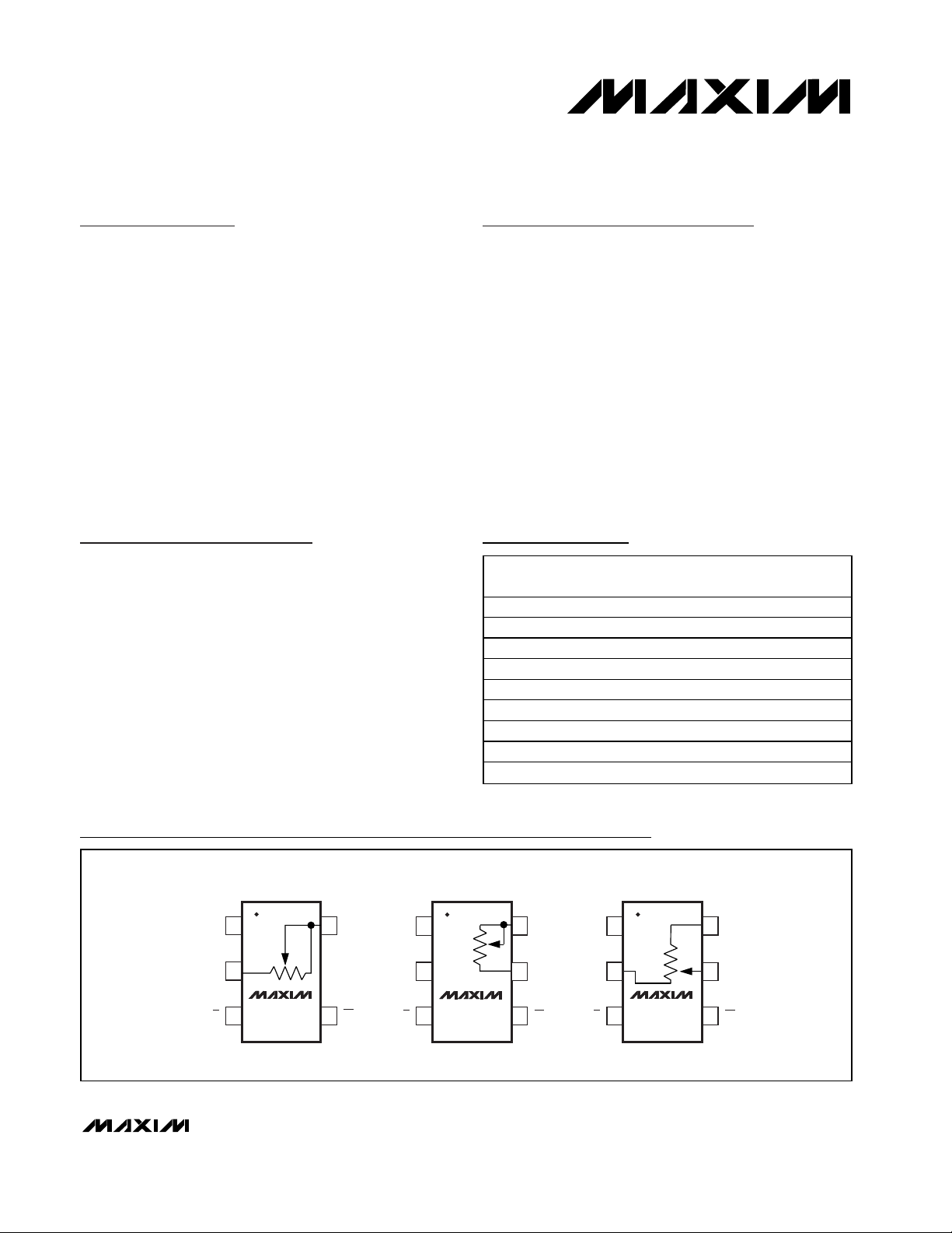
The MAX5462/MAX5465/MAX5468 are configured as
potentiometers. The rest of the devices in this family are
configured as variable resistors. See Pin Configurations
for part functionality.
Three resistance values are available: 10kΩ (MAX5466/
MAX5467/MAX5468), 50kΩ (MAX5463/MAX5464/
MAX5465), and 100kΩ (MAX5460/MAX5461/MAX5462).
The MAX5460–MAX5465 (100kΩ and 50kΩ) are available in space-saving 5-pin and 6-pin SC70 packages.
The MAX5466/MAX5467/MAX5468 (10kΩ) are available
in 5-pin and 6-pin SOT23 packages.
Applications
LCD Screen Adjustment
Volume Control
Mechanical Potentiometer Replacement
Gain Adjustment
Line Impedance Matching
Features
♦ Miniature SC70 and SOT23 Packages
♦ 0.3µA Ultra-Low Supply Current
♦ +2.7V to +5.5V Single-Supply Operation
♦ Glitchless Switching Between Resistor Taps
♦ Power-On Reset to Midscale
♦ 2-Wire Up/Down Serial Interface
♦ 10kΩ, 50kΩ, and 100kΩ Resistance Values
MAX5460–MAX5468
32-Tap FleaPoT™, 2-Wire Digital
Potentiometers
________________________________________________________________ Maxim Integrated Products 1
Pin Configurations
Ordering Information
19-1956; Rev 2; 9/02
For pricing, delivery, and ordering information, please contact Maxim/Dallas Direct! at
1-888-629-4642, or visit Maxim’s website at www.maxim-ic.com.
Functional Diagram appears at end of data sheet.
FleaPoT is a trademark of Maxim Integrated Products Inc.
PART
MAX5460EXK -40°C to +85°C 5 SC70 ACA 100
MAX5461EXT -40°C to +85°C 6 SC70 AAP 100
MAX5462EXT -40°C to +85°C 6 SC70 AAQ 100
MAX5463EXK -40°C to +85°C 5 SC70 ACB 50
MAX5464EXT -40°C to +85°C 6 SC70 AAR 50
MAX5465EXT -40°C to +85°C 6 SC70 AAS 50
MAX5466EUK
MAX5467EUT -40°C to +85°C 6 SOT23 AARH 10
MAX5468EUT -40°C to +85°C 6 SOT23 AARI 10
TEMP
RANGE
-40°C to +85°C 5 SOT23 ADQQ 10
PINPACKAGE
TOP
MARK
R (kΩ)
TOP VIEW
15HV
DD
2
GND
MAX5460
34
MAX5463
MAX5466
SOT23, SC70
CSU/D
16HV
DD
2
GND
MAX5461
34
MAX5464
MAX5467
SOT23, SC70
L5
CSU/D
16HV
DD
2
GND
MAX5462
34
MAX5465
MAX5468
SOT23, SC70
W5
CSU/D
MAX5460–MAX5468
32-Tap FleaPoT™, 2-Wire Digital
Potentiometers
2 _______________________________________________________________________________________
ABSOLUTE MAXIMUM RATINGS
ELECTRICAL CHARACTERISTICS
(VDD= +2.7V to +5.5V, VH= VDD, VL= 0, TA= -40°C to +85°C. Typical values are at VDD= +2.7V, TA= +25°C, unless
otherwise noted.)
Stresses beyond those listed under “Absolute Maximum Ratings” may cause permanent damage to the device. These are stress ratings only, and functional
operation of the device at these or any other conditions beyond those indicated in the operational sections of the specifications is not implied. Exposure to
absolute maximum rating conditions for extended periods may affect device reliability.
VDDto GND..............................................................-0.3V to +6V
All Other Pins to GND.................................-0.3V to (VDD+ 0.3)V
Input and Output Latch-Up Immunity.............................±200mA
Maximum Continuous Current into H, L, and W
MAX5460/MAX5461/MAX5462 (100kΩ) .......................±0.6mA
MAX5463/MAX5464/MAX5465 (50kΩ) .........................±1.3mA
MAX5466/MAX5467/MAX5468 (10kΩ) .........................±1.3mA
Continuous Power Dissipation (TA= +70°C)
5-pin SC70 (derate 3.1mW/°C above TA= +70°C)..........247mW
5-pin SOT23 (derate 7.1mW/°C above TA= +70°C)........571mW
6-pin SC70 (derate 3.1mW/°C above TA= +70°C) ..........245mW
6-pin SOT23 (derate 8.7mW/°C above T
A
= +70°C).....695.7mW
Operating Temperature Range ...........................-40°C to +85°C
Junction Temperature......................................................+150°C
Storage Temperature Range .............................-65°C to +150°C
Soldering Temperature (soldering, 10s) ..........................+300°C
DC PERFORMANCE
Resolution 32 Taps
End-to-End Resistance
End-to-End Resistance Tempco TC
Ratiometric Resistance Tempco 5 ppm/°C
Integral Nonlinearity INL ±0.5 ±1 LSB
Differential Nonlinearity DNL ±1 LSB
Full-Scale Error ±0.1 LSB
Zero-Scale Error 1 LSB
Wiper Resistance R
DIGITAL INPUTS
Input High Voltage V
Input Low Voltage V
TIMING CHARACTERISTICS (Figures 1, 2)
U/D Mode to CS Setup t
CS to U/D Step Setup t
CS to U/D Step Hold t
U/D Step Low Period t
U/D Step High Period t
Up/Down Toggle Rate (Note 1) f
Output Settling Time (Note 2) t
PARAMETER SYMBOL CONDITIONS MIN TYP MAX UNITS
MAX5460/MAX5461/MAX5462 75 100 125
MAX5463/MAX5464/MAX5465 37.5 50 62.5
MAX5466/MAX5467/MAX5468 7.5 10 12.5
R
MAX5460–MAX5465 600 1200
W
MAX5466/MAX5467/MAX5468 160 240
IH
IL
CU
CI
IC
IL
IH
TOGGLE
SETTLE
100kΩ var i ab l e r esi stor confi g ur ati on, C L = 10p F1
100kΩ p otenti om eter confi g ur ati on, C L = 10p F 0.25
0.7 x V
DD
25 ns
50 ns
25 ns
25 ns
25 ns
35 ppm/°C
0.3 x V
DD
1 MHz
kΩ
Ω
V
V
µs
MAX5460–MAX5468
32-Tap FleaPoT™, 2-Wire Digital
Potentiometers
_______________________________________________________________________________________ 3
Typical Operating Characteristics
(TA = +25°C, unless otherwise noted.)
Note 1: Up/Down Toggle Rate:
Note 2: Typical settling times are dependent on end-to-end resistance.
Note 3: Supply current taken while changing wiper tap, f
TOGGLE
= 1MHz.
Note 4: Supply current taken while wiper position is fixed.
ELECTRICAL CHARACTERISTICS (continued)
(VDD= +2.7V to +5.5V, VH= VDD, VL= 0, TA= -40°C to +85°C. Typical values are at VDD= +2.7V, TA= +25°C, unless
otherwise noted.)
PARAMETER SYMBOL CONDITIONS MIN TYP MAX UNITS
POWER SUPPLIES
Supply Voltage V
Active Supply Current (Note 3) I
Standby Supply Current (Note 4) I
f
TOGGLE
=
1
t
SETTLE
DD
DD
SD
VDD = +5V 0.3 1 µA
2.7 5.5 V
25 µA
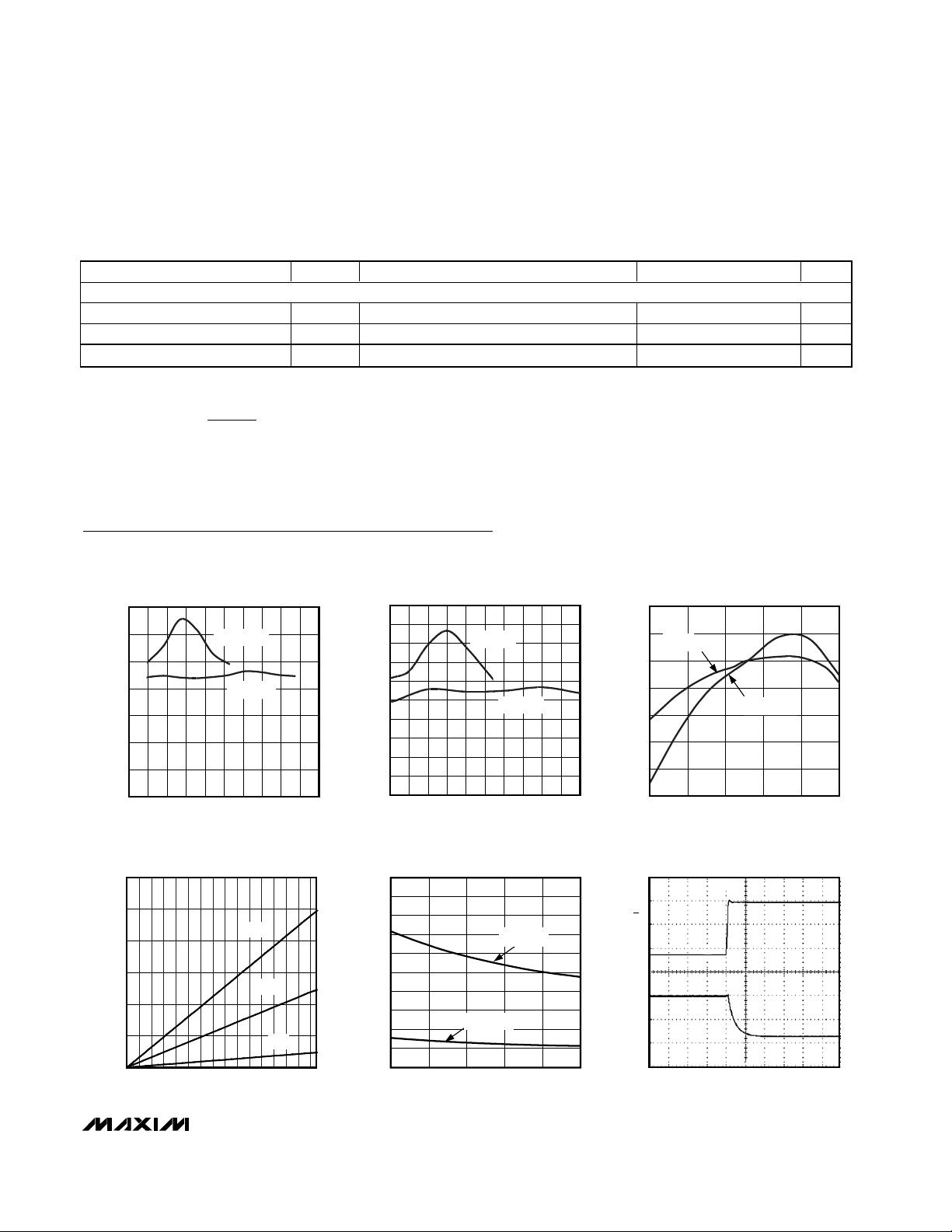
WIPER RESISTANCE vs. WIPER VOLTAGE
(MAX5460–MAX5465)
700
600
500
400
300
WIPER RESISTANCE (Ω)
200
100
0
0 2.01.0 3.0 4.00.5 2.51.5 3.5 4.5 5.0
VDD = +2.7V
VDD = +5V
WIPER VOLTAGE (V)
W-TO-L RESISTANCE
vs. TAP POSITION
120
100
80
60
RESISTANCE (kΩ)
40
20
0
1357911131517 19 21 23 25 27 29 31
TAP POSITION
100kΩ
50kΩ
10kΩ
MAX5460 toc01
MAX5460 toc04
WIPER RESISTANCE vs. WIPER VOLTAGE
(MAX5466/MAX5467/MAX5468)
200
180
160
140
120
100
80
60
WIPER RESISTANCE (Ω)
40
20
0
0 1.0 1.5 2.00.5 2.5 3.0 3.5 4.54.0 5.0
VDD = +2.7V
VDD = +5V
WIPER VOLTAGE (V)
SUPPLY CURRENT vs. TEMPERATURE
0.50
0.45
0.40
0.35
0.30
0.25
0.20
CURRENT (µA)
0.15
0.10
0.05
0.00
-40 10-15 35 60 85
TEMPERATURE (°C)
VDD = +5V
VDD = +2.7V
END-TO-END RESISTANCE % CHANGE
0.10
0.05
MAX5460 toc02
-0.05
-0.10
-0.15
-0.20
END-TO-END RESISTANCE % CHNAGE
-0.25
10kΩ
0
-40 10-15 35 60 85
TAP-TO-TAP SWITCHING TRANSIENT
MAX5460 toc05
U/D
2V/div
OUTPUT
W
100mV/div
vs. TEMPERATURE
50kΩ, 100kΩ
TEMPERATURE (°C)
(MAX5460)
200ns/div
MAX5460 toc03
MAX5460 toc06

MAX5460–MAX5468
32-Tap FleaPoT™, 2-Wire Digital
Potentiometers
4 _______________________________________________________________________________________
Typical Operating Characteristics (continued)
(TA = +25°C, unless otherwise noted.)
Pin Description
R-DNL ERROR vs. INPUT CODE (100kΩ)
0.08
0.06
0.04
0.02
0
-0.02
R-DNL (LSB)
-0.04
-0.06
-0.08
-0.10
010155 202530
INPUT CODE (DECIMAL)
MAX5460 toc07
R-INL ERROR vs. INPUT CODE (100kΩ)
0.10
0.08
0.06
0.04
0.02
0
R-INL (LSB)
-0.02
-0.04
-0.06
-0.08
-0.10
0 5 10 15 20 25 30
INPUT CODE (DECIMAL)
MAX5460 toc08
R-DNL ERROR vs. INPUT CODE (50kΩ)
0.04
0.02
0
-0.02
-0.04
-0.06
R-DNL (LSB)
-0.08
-0.10
-0.12
-0.14
010155202530
INPUT CODE (DECIMAL)
MAX5460 toc09
R-INL ERROR vs. INPUT CODE (50kΩ)
0.20
0.15
0.10
0.05
R-INL LSB
0
-0.05
-0.10
01520510 2530
INPUT CODE (DECIMAL)
MAX5460 toc10
-0.05
R-DNL LSB
-0.10
-0.15
-0.20
-0.25
PIN
MAX5460
MAX5463
MAX5466
MAX5461
MAX5464
MAX5467
MAX5462
MAX5465
MAX5468
111V
2 2 2 GND Ground
333U/D
444CS
5 6 6 H High Terminal of Resistor
— 5 — L Low Terminal of Resistor
—— 5 W Wiper Terminal of Resistor
R-DNL ERROR vs. INPUT CODE (10kΩ)
0.15
0.10
0.05
0
010155
INPUT CODE (DECIMAL)
NAME FUNCTION
DD
R-INL ERROR vs. INPUT CODE (10kΩ)
0.30
0.25
MAX5460 toc11
0.20
0.15
0.10
0.05
R-INL (LSB)
0
-0.05
-0.10
-0.15
25 30
20
010155202530
INPUT CODE (DECIMAL)
Power Supply
Up/Down Control Input. With CS low, a low-to-high
transition increments or decrements the wiper position.
Chip Select Input. A high-to-low CS transition
determines the mode: increment if U/D is high, or
decrement if U/D is low.
MAX5460 toc12

MAX5460–MAX5468
32-Tap FleaPoT™, 2-Wire Digital
Potentiometers
_______________________________________________________________________________________ 5
Detailed Description
The MAX5460–MAX5468 consist of a fixed resistor and a
wiper contact with 32-tap points that are digitally controlled through a 2-wire serial interface. Three resistance
values are available: 10kΩ (MAX5466/MAX5467/
MAX5468), 50kΩ (MAX5463/MAX5464/MAX5465), and
100kΩ (MAX5460/MAX5461/MAX5462).
The MAX5462/MAX5465/MAX5468 are designed to operate as potentiometers. In this configuration, the low terminal of the resistor array is connected to ground (pin 2).
The MAX5461/MAX5464/MAX5467 perform as variable
resistors. In these devices, the wiper terminal and high
terminal of the resistor array are connected at pin 5.
The MAX5460/MAX5463/MAX5466 are similar variable
resistors, except the low terminal is connected to
ground (pin 2).
Digital Interface Operation
The MAX5460–MAX5468 have two modes of operation
when the serial interface is active: increment and
decrement mode. The serial interface is only active
when CS is low.
The CS and U/D inputs control the position of the wiper
along the resistor array. When CS transitions from high to
low, the part will go into increment mode if U/D is high,
and into decrement mode if U/D is low. Once the mode is
set, the device will remain in that mode until CS goes high
again. A low-to-high transition at the U/D pin will increment or decrement the wiper position depending on the
current mode (Figures 1 and 2).
When the CS input transitions to high (serial interface
inactive), the value of the counter is stored and the
wiper position is maintained.
Note that when the wiper reaches the maximum (or minimum) tap position, the wiper will not wrap around to the
minimum (or maximum) position.
Figure 1. Serial Interface Timing Diagram, Increment Mode
Figure 2. Serial Interface Timing Diagram, Decrement Mode
CS
t
CU
t
IL
U/D
t
CI
t
SETTLE
W
t
IC
t
IH
t
SETTLE
NOTE: "W" IS NOT A DIGITAL SIGNAL. IT REPRESENTS WIPER TRANSITIONS.
CS
t
CU
U/D
t
t
SETTLE
CI
W
NOTE: "W" IS NOT A DIGITAL SIGNAL. IT REPRESENTS WIPER TRANSITIONS.
t
t
IH
t
IL
t
SETTLE
IC

MAX5460–MAX5468
32-Tap FleaPoT™, 2-Wire Digital
Potentiometers
6 _______________________________________________________________________________________
Power-On Reset
All parts in this family feature power-on reset (POR) circuitry that sets the wiper position to midscale at powerup. By default, the chip is in the increment mode.
Applications Information
The MAX5460–MAX5468 are intended for circuits
requiring digitally controlled adjustable resistance,
such as LCD contrast control, where voltage biasing
adjusts the display contrast.
Controlling a Switch-Mode
LCD Bias Generator
Figure 3 shows an application where the variable resistor is used with a MAX1771 to make an adjustable positive LCD-bias circuit. The output of the MAX1771 is a
positive voltage that is digitally controlled through the
MAX5461/MAX5464/MAX5467. Similarly, Figure 4
shows the application of the variable resistor in a digitally controlled negative LCD-bias circuit along with the
MAX774/MAX775/MAX776.
Alternative Positive
LCD Bias Control
Alternatively, use an op amp to provide buffering and
gain to the output of the MAX5462/MAX5465/MAX5468.
Connect the mechanical potentiometer to the positive
input of a noninverting op amp (Figure 5) to select a
portion of the input signal by digitally controlling the
wiper terminal. Figure 6 shows a similar circuit for the
MAX5461/MAX5464/MAX5467.
Adjustable Gain
Figure 7 shows how to use the variable resistor to digitally adjust the gain of a noninverting op amp configuration. Connect the MAX5461/MAX5464/MAX5467 in
series with a resistor to ground to form the adjustable
gain control of a noninverting amplifier. The MAX5460–
MAX5468 have a low 5ppm/°C ratiometric tempco that
allows for a very stable adjustable gain configuration
over temperature.
Figure 3. Adjustable Positive LCD Bias
Figure 4. Adjustable Negative LCD Bias
VIN = 5V
68µF
0.1µF
V
C3
REF
C1
= 1.5V
C2
0.1µF
2
REF
SHDN
AGND
V+
MAX1771
GND
7
5
4
6
EXT
CS
FB
MAX5461
MAX5464
MAX5467
22µH
1
8
3
V
OUT(MAX)
V
V
OUT(MIN)
V
L1
1N5817-22
N
MTD20N03HDL
R
SENSE
40mΩ
R1
= R2
R1
REF
=
R1 + R
REF
D1
C4
300µF
R2
C5
R
VAR
+ 1
R2 )
(
VAR(MAX)
V
OUT
= 12V
AT 0.5A
+ 1
V
IN
150µF
C1
C2
0.1µF
MAX5461
MAX5464
MAX5467
V
= R2
OUT(MAX)
R1 V
V
REF
V
- VFB
REF
≥ 5µA (FOR 2% GAIN-SETTING ACCURACY)
R1 + R
VAR
1
OUT V+
3
R2
R1
,
R
VAR
C3
0.1µF
V
OUT(MIN)
2
4
REF
SHDN
FB EXT
REF
= R2
R1 + R
5
6
CS
7
MAX774
MAX775
MAX776
L1
GND
8
VAR
22µH
* MAX774 = 330µF, 10V
MAX775/MAX776 = 120µF, 20V
R3
0.07Ω
Q1
Si9435
P
1N5822/
MBR340
C4*
V
OUT

MAX5460–MAX5468
32-Tap FleaPoT™, 2-Wire Digital
Potentiometers
_______________________________________________________________________________________ 7
Figure 5. Positive LCD Bias Control
Figure 6. Positive LCD Bias Control
Figure 7. Adjustable Gain Circuit
+5V
H
W
L
MAX5462
MAX5465
MAX5468
V
IN
H
L
a)
30V
V
CC
MAX5461
MAX5464
MAX5467
+5V
H
30V
V
OUT
L
MAX5461
MAX5464
MAX5467
V
OUT
V
CC
V
V
OUT
b)
IN
W
L
MAX5462
MAX5465
MAX5468
H
V
OUT

MAX5460–MAX5468
32-Tap FleaPoT™, 2-Wire Digital
Potentiometers
8 _______________________________________________________________________________________
Chip Information
TRANSISTOR COUNT: 792
UP/DN
COUNTER
V
DD
GND
CS
H
L
W
U/D
32-POSITION
DECODER
MAX5460–MAX5468
Functional Diagram

MAX5460–MAX5468
32-Tap FleaPoT™, 2-Wire Digital
Potentiometers
_______________________________________________________________________________________ 9
Package Information
(The package drawing(s) in this data sheet may not reflect the most current specifications. For the latest package outline information
go to www.maxim-ic.com/packages.)
SC70, 5L.EPS
SOT5L.EPS

MAX5460–MAX5468
32-Tap FleaPoT™, 2-Wire Digital
Potentiometers
Maxim cannot assume responsibility for use of any circuitry other than circuitry entirely embodied in a Maxim product. No circuit patent licenses are
implied. Maxim reserves the right to change the circuitry and specifications without notice at any time.
10 ____________________Maxim Integrated Products, 120 San Gabriel Drive, Sunnyvale, CA 94086 408-737-7600
© 2002 Maxim Integrated Products Printed USA is a registered trademark of Maxim Integrated Products.
Package Information (continued)
(The package drawing(s) in this data sheet may not reflect the most current specifications. For the latest package outline information
go to www.maxim-ic.com/packages.)
6LSOT.EPS
SC70, 6L.EPS
 Loading...