

Page 1
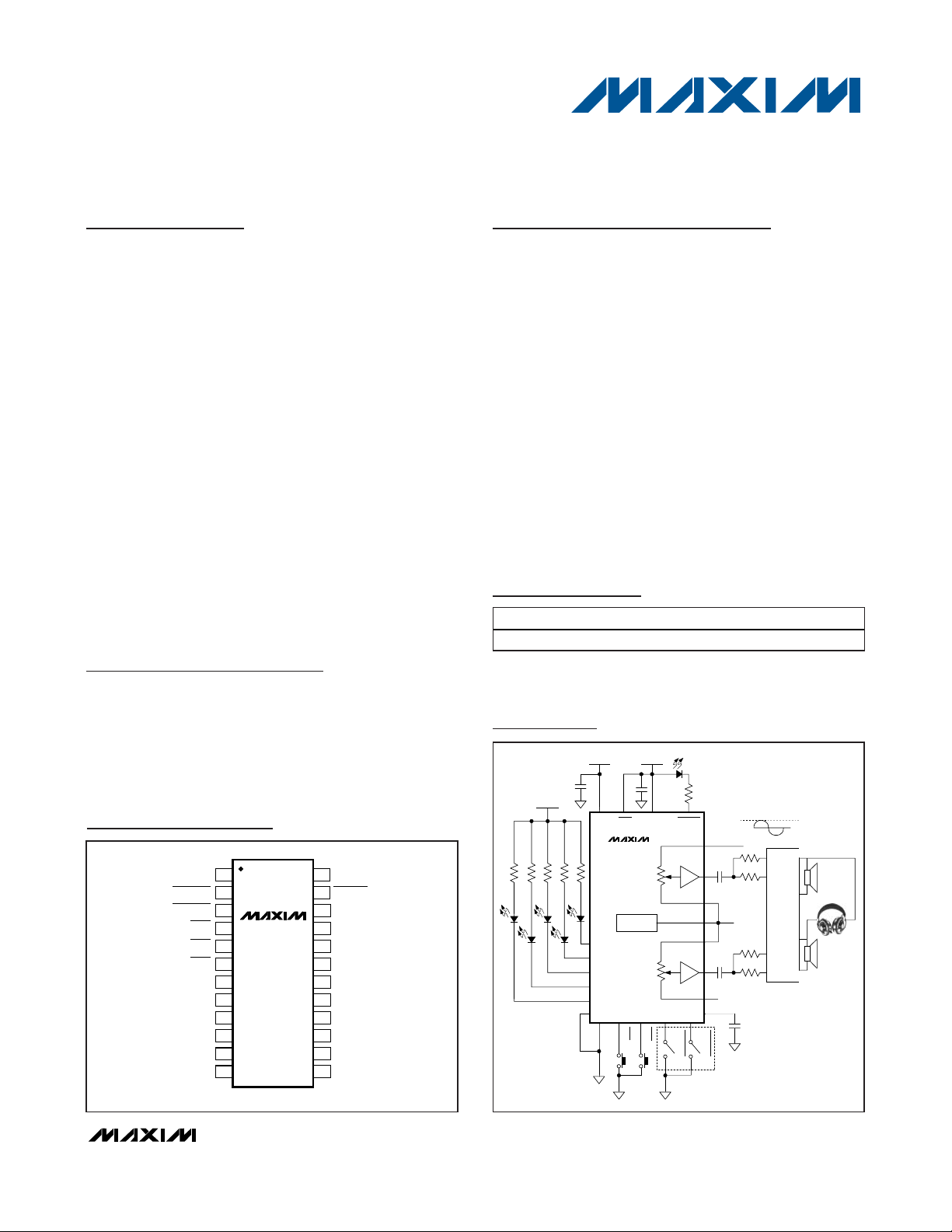
General Description
The MAX5440 dual, 40kΩ logarithmic taper volume control features a debounced up/down interface for use
with a simple rotary encoder without using a microcontroller (µC). Each potentiometer has 32 log-spaced tap
points with a buffered wiper output and replaces
mechanical potentiometers. An integrated bias generator provides the required ((VDD+ VSS) / 2) bias voltage,
eliminating the need for costly external op-amp circuits
in unipolar audio applications. A mode-indicator LED
output specifies volume or balance control. Five integrated LED drivers indicate volume level or balance settings, depending on the status of the mode indicator.
The MAX5440 includes debounced pushbutton inputs
for mute and mode. The mute input allows a single
pushbutton to change between volume control and the
-90dB (typ) mute setting. The mode input toggles
between volume and balance control. A click-and-pop
suppression feature minimizes the audible noise generated by wiper transitions. The MAX5440 provides a
nominal temperature coefficient of 35ppm/°C end-toend and 5ppm/°C, ratiometrically. The MAX5440 is
available in a 24-pin SSOP package and is specified for
operation over the -40°C to +85°C extended temperature range.
Applications
Stereo Volume Control
Desktop Speakers
Multimedia Docking Stations
Set-Top Boxes
Automotive Back-Seat Multimedia
Features
♦ Logarithmic Taper Volume Control with (31) 2dB
Steps
♦ Low-Power Wiper Buffers Provide 0.003% THD
♦ Single +2.7V to +5.5V or Dual ±2.7V Supply
Voltage Operation
♦ Low 0.5µA Shutdown Supply Current
♦ Integrated Bias Voltage Generator
♦ Five-Segment LED Volume/Balance Indicator
♦ Clickless Switching
♦ 40kΩ End-to-End Fixed Resistance Value
♦ Mute Function Toggles to -90dB (typ)
♦ Power-On Reset to -12dBFS Wiper Position
MAX5440
Stereo Volume Control
with Rotary Encoder Interface
________________________________________________________________
Maxim Integrated Products
1
Pin Configuration
V
DD
V
SS
(V
DD + VSS
) / 2
(V
DD + VSS
) / 2
V
LOGIC
V
PEAK
H1
L1
W1
SHDN
LEFT INPUT
RIGHT INPUT
MODEIND
HEADPHONE
DRIVER
L0
H0
W0
V
LOGIC
LEDIND4
LEDIND3
LEDIND0
GND
MUTE
MODE
RENCODEA
RENCODEB
LEDIND1
LEDIND2
ROTARY
ENCODER
MIDBIAS
BIAS
MAX5440
Typical Operating Circuit
19-0542; Rev 2; 11/08
Ordering Information
For price, delivery, and to place orders, please contact Maxim Distribution at 1-888-629-4642,
or visit Maxim’s website at www.maxim-ic.com.
PART TEMP RANGE PIN-PACKAGE
MAX5440EAG -40°C to +85°C 24 SSOP
TOP VIEW
V
LOGIC
RENCODEB
RENCODEA
2
3
MUTE
4
MODE
SHDN
GND
H0
L0
W0
MIDBIAS
BIAS
MAX5440
5
6
7
8
9
11
12
SSOP
1
24
23
22
21
20
19
18
17
16
1510W1
14
13
GND
MODEIND
LEDIND4
LEDIND3
LEDIND2
LEDIND1
LEDIND0
H1
L1
V
SS
V
DD
Page 2
MAX5440
Stereo Volume Control
with Rotary Encoder Interface
ABSOLUTE MAXIMUM RATINGS
Stresses beyond those listed under “Absolute Maximum Ratings” may cause permanent damage to the device. These are stress ratings only, and functional
operation of the device at these or any other conditions beyond those indicated in the operational sections of the specifications is not implied. Exposure to
absolute maximum rating conditions for extended periods may affect device reliability.
SHDN, MUTE, RENCODEA, RENCODEB,
and MODE to GND............................-0.3V to (V
LOGIC
+ 0.3V)
H_, L_, and W_ to V
SS
...............................-0.3V to (VDD+ 0.3V)
LEDIND_, MODEIND to GND................-0.3V to (V
LOGIC
+ 0.3V)
MIDBIAS, BIAS to V
SS
......................(VSS- 0.3V) to (VDD+ 0.3V)
V
LOGIC
to GND...........................................-0.3V to (VDD+ 0.3V)
V
DD
to GND..............................................................-0.3V to +6V
V
DD
to VSS................................................................-0.3V to +6V
V
SS
to GND...............................................................-3V to +0.3V
Input and Output Latchup Immunity...............................±200mA
Continuous Power Dissipation (T
A
= +70°C)
24-Pin SSOP (derate 12.3mW/°C above +70°C) ......987.7mW
Operating Temperature Range ...........................-40°C to +85°C
Junction Temperature......................................................+150°C
Storage Temperature Range .............................-60°C to +150°C
Lead Temperature (soldering, 10s) .................................+300°C
ELECTRICAL CHARACTERISTICS
(VDD= +2.7V to +5.5V, VSS= V
GND
= 0, 2.7V ≤ (VDD- VSS) ≤ 5.5V, V
LOGIC
= +2.7V to VDD, V
H_
= VDD, V
L_
= VDD/ 2, TA= T
MIN
to
T
MAX
, unless otherwise specified. Typical values are at TA= +25°C.) (Note 1)
2 _______________________________________________________________________________________
PARAMETER SYMBOL CONDITIONS MIN TYP MAX UNITS
End-to-End Resistance R 36 40 52 kΩ
Absolute Tolerance ±0.25 dB
Tap-to-Tap Tolerance ±0.1 dB
Total Harmonic Distortion Plus
Noise
Channel Isolation 100 dB
Interchannel Matching ±0.5 dB
Mute Attenuation SHDN = V
Power-Supply Rejection Ratio PSRR Input referred, 217Hz, 100mV
H Terminal Capacitance C
L Terminal Capacitance C
End-to-End Resistance
Ratiometric Resistance
Bandwidth, -3dB f
Output Noise e
WIPER BUFFER
Output Voltage Swing V
Output Current 3mA
Output Resistance R
DC Offset -14 ±2 +14 mV
INTEGRATED BIAS GENERATOR
Output Voltage I
V
= ( V
H _
= ∞ to V
V
= ( V
H _
= ∞ to V
R
L
V
= 5V,V
THD+N
DD
(VDD / 2) + 1V
10kΩ to V
= 5V,V
V
DD
2) + 1.5V
to V
MIDBIAS
H
L
CUTOFFCW
n
O
OWB
= 33pF 100 kHz
20Hz to 20kHz 3.2 µV
RL = 10kΩ to V
= 1mA
LOAD
/ 2) + 1V
D D
= V
L_
D D
/ 2) + 1.5V
D D
= V
L_
= 0V, V
SS
RMS
MIDBIAS
= 0V, V
SS
1kHz tap at top, RL = 10kΩ
RM S ,
, 20Hz to 20kHz
DD
MIDBIAS
, 1kH z tap at top , R
RM S
/ 2, 20H z to 20kH z
, 1kH z tap at top ,
RM S
/ 2, 20H z to 20kH z
D D
= 1.5V, V
L_
H_
, 1kHz tap at top, RL =
=
L
0.004
0.006
0.004
, 20Hz to 20kHz
= 5V, V
L_
H _
= ( V
D D
/
0.006
90 dB
P-P
on V
DD
-60 dB
5pF
7pF
35 ppm/°C
5 ppm/°C
VDD - 0.2 V
110Ω
(V
DD
) / 2
V
SS
- 30mV
(V
+
DD
V
/ 2
SS
( V
+
)
V
S S
+
D D
) / 2 +
30m V
%
RMS
V
Page 3
MAX5440
Stereo Volume Control
with Rotary Encoder Interface
ELECTRICAL CHARACTERISTICS (continued)
(VDD= +2.7V to +5.5V, VSS= V
GND
= 0, 2.7V ≤ (VDD- VSS) ≤ 5.5V, V
LOGIC
= +2.7V to VDD, V
H_
= VDD, V
L_
= VDD/ 2, TA= T
MIN
to
T
MAX
, unless otherwise specified. Typical values are at TA= +25°C.) (Note 1)
Note 1: Parameters are 100% production tested at +85°C and limits through temperature are guaranteed by design.
Note 2: The device draws current in excess of the specified supply current when the digital inputs are driven with voltages between
(V
DD
- 0.5V) and (GND + 0.5V). See Digital Supply Current vs. Digital Input Voltage in the
Typical Operating Characteristics
.
Note 3: Shutdown refers to the SHDN input being asserted low. Standby refers to SHDN not being asserted and all I/O inactive.
Note 4: Supply current measured with the wiper position fixed.
_______________________________________________________________________________________ 3
PARAMETER SYMBOL CONDITIONS MIN TYP MAX UNITS
Power-Supply Rejection Ratio PSRR
Maximum Load To V
Output Resistance R
OBR
1kHz, 100mV on VDD, 1µF on BIAS 60 dB
BR
or GND 3 kΩ
DD
6 Ω
CONTACT INPUTS (MUTE, MODE, RENCODEA, RENCODEB)
Internal Pullup Resistor R
Single Pulse Input Low Time t
Repetitive Input Pulse Separation t
Timeout Period t
PULLUP
CPW
IPWS
WS
22 ms
66 ms
Click/pop suppression inactive 32 ms
45 kΩ
DIGITAL INPUTS (MUTE, MODE, RENCODEA, RENCODEB, SHDN)
Input High Voltage (Note 2) V
Input Low Voltage (Note 2) V
3.6V < V
IH
2.7V ≤ V
3.6V < V
IL
2.7V ≤ V
≤ 5.5V 2.4
LOGIC
≤ 3.6V 2.0
LOGIC
≤ 5.5V 0.8
LOGIC
≤ 3.6V 0.6
LOGIC
V
V
Input Leakage Current Inputs unconnected -1 +1 µA
Input Capacitance 5pF
POWER SUPPLIES
Supply Voltage V
DD
Negative Power Supply V
Supply Voltage Difference V
Active Supply Current I
S tand b y S up p l y C ur r ent ( N otes 3, 4) I
Shutdown Supply Current I
Power-Up Time t
Logic Supply Voltage V
DD
STBY
SHDN
PU
LOGICVSS
Logic Active Supply Current I
Logic Standby Supply Current I
Logic Shutdown Current I
LSTBY
LSHDN
VSS = 0 2.7 5.5 V
VDD = +2.7V -2.7 0 V
SS
- V
DD
SS
VDD = +5V, VSS = 0 1.3
VDD = +2.7V, VSS = -2.7V 1.3
(Note 3) 1 µA
Click/pop suppression inactive 50 ms
= 0 2.7 V
V
L
RENCODEA = VRENCODEB
= 0V 320 µA
(Note 4) 1 µA
5.5 V
1.4 mA
mA
DD
V
1µA
LED INDICATORS (LEDIND0–LEDIND4, MODEIND)
Output Low Voltage V
OL
LOGIC
V
LOGIC
= 2.7V, I
= 5.5V, I
= 10mA 0.4
SINK
= 10mA 0.2
SINK
V
V
Output Leakage Current 0.1 10 µA
Output Capacitance 3pF
Maximum Sink Current 150 mA
Page 4
MAX5440
Stereo Volume Control
with Rotary Encoder Interface
4 _______________________________________________________________________________________
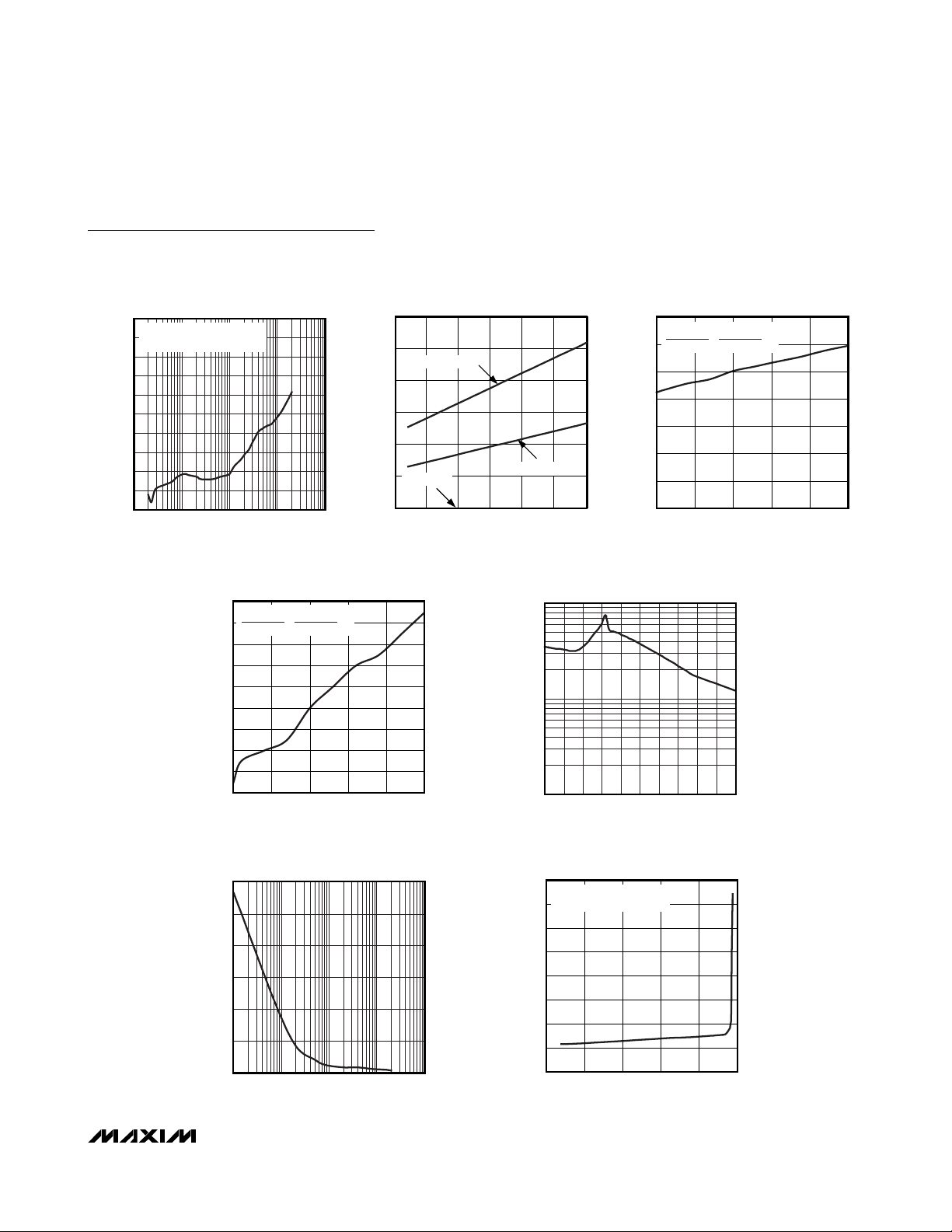
Typical Operating Characteristics
(TA = +25°C, unless otherwise noted.)
-70
-60
-40
-50
-20
-10
-30
0
08124 1620242832
ATTENUATION vs. TAP POSITION
MAX5440 toc01
TAP POSITION
ATTENUATION (dB)
-0.25
-0.15
-0.20
-0.05
-0.10
0.05
0
0.10
-40 10-15 35 60 85
END-TO-END RESISTANCE % CHANGE
vs. TEMPERATURE
MAX5440 toc02
TEMPERATURE (°C)
END-TO-END RESISTANCE CHANGE (%)
1.38
1.41
1.40
1.39
1.42
1.43
1.44
1.45
1.46
1.47
1.48
-40 10-15 35 60 85
TOTAL SUPPLY CURRENT
vs. TEMPERATURE
MAX5440 toc03
TEMPERATURE (°C)
TOTAL SUPPLY CURRENT (mA)
V
LOGIC
= VDD = 5.5V
WIPER
TRANSITION
FROM -2dB
TO -4dB
20ms/div
WIPER SWITCHING TRANSIENT
MAX5440 toc04
RENCODEA
RENCODEB
51ms
0
20
10
40
30
60
50
70
90
80
100
08124 1620242832
WIPER-TO-END TERMINAL VOLTAGE
vs. TAP POSITION
MAX5440 toc05
TAP POSITION
NOMINAL END-TO-END VOLTAGE (%V
HL
)
V
HW
V
WL
-2.8
-2.0
-2.4
-0.4
-0.8
-1.2
-1.6
0.8
0.4
0
0.01 10.1 10 100 1000
FREQUENCY RESPONSE
MAX5440 toc06
FREQUENCY (kHz)
RESPONSE (dB)
VH_ = 2.5 ±1V
RMS
, VL_ = 2.5V, CL_ = 33pF
W_ SET TO 0dB
-8.8
-8.0
-8.4
-6.4
-6.8
-7.6
-7.2
-5.6
-6.0
-5.2
0.01 10.1 10 100 1000
FREQUENCY RESPONSE
MAX5440 toc07
FREQUENCY (kHz)
RESPONSE (dB)
W_ SET TO -6dB
VH_ = 2.5 ±1V
RMS
, VL_ = 2.5V, CL_ = 33pF
0.001
0.01
0.1
0.001 0.10.01 1 10 100
THD+N vs. FREQUENCY
MAX5440 toc08
FREQUENCY (kHz)
W_ SET AT -2dB
THD+N (%)
VDD = 2.5V
V
SS
= -2.5V
L_ = V
MIDBIAS
H_ = V
MIDBIAS
+ 1V
RMS
W_ SET AT -6dB
W_ SET AT 0dB
0.001
0.01
0.1
0.001 0.10.01 1 10 100
THD+N vs. FREQUENCY
MAX5440 toc09
FREQUENCY (kHz)
THD+N (%)
VDD = 5.0V
V
SS
= GND
L_ = V
MIDBIAS
H_ = V
MIDBIAS
+ 1V
RMS
W_ SET AT -2dB
W_ SET AT -6dB
W_ SET AT 0dB
Page 5
MAX5440
Stereo Volume Control
with Rotary Encoder Interface
-75
-65
-70
-45
-50
-55
-60
-35
-40
-25
-30
0.01 10.1 10 100
POWER-SUPPLY REJECTION RATIO
vs. FREQUENCY
MAX5440 toc10
FREQUENCY (kHz)
RESPONSE (dB)
V
DD_
= 5V ±100mV
P-P
, VH = 5V
V
L_
= 2.5V, W_ SET TO -6dB
0
100
50
200
150
250
300
LOGIC SUPPLY CURRENT
vs. LOGIC SUPPLY VOLTAGE
MAX5440 toc11
LOGIC SUPPLY VOLTAGE (V)
LOGIC SUPPLY CURRENT (µA)
2.5 3.5 4.03.0 4.5 5.0 5.5
ACTIVE CURRENT
STANDBY CURRENT
SHUTDOWN
0
100
50
200
150
300
250
350
-40 10-15 35 60 85
ACTIVE LOGIC SUPPLY CURRENT
vs. TEMPERATURE
MAX5440 toc12
TEMPERATURE (°C)
LOGIC SUPPLY CURRENT (µA)
VDD = V
LOGIC
= 5.5V,
RENCODEA = RENCODEB = 0
1.1752
1.1756
1.1754
1.1762
1.1760
1.1758
1.1768
1.1766
1.1764
1.1770
-40 10-15 356085
ACTIVE SUPPLY CURRENT
vs. TEMPERATURE
MAX5440 toc13
TEMPERATURE (°C)
SUPPLY CURRENT (mA)
VDD = V
LOGIC
= 5.5V,
RENCODEA = RENCODEB = 0
10
100
1000
0 0.5 2.0 2.51.0 1.5 3.0 3.5 4.0 4.5 5.0
DIGITAL SUPPLY CURRENT
vs. DIGITAL INPUT VOLTAGE
MAX5440 toc14
DIGITAL INPUT VOLTAGE (V)
DIGITAL SUPPLY CURRENT (µA)
200
0
400
800
600
1000
1200
0.01 10.1 10 100
SPECTRAL NOISE DENSITY
MAX5440 toc15
FREQUENCY (kHz)
NOISE (nV/√Hz)
0
1
2
3
4
5
6
7
8
2.5 3.0 3.5 4.0 4.5 5.0
SUPPLY CURRENT
vs. INPUT VOLTAGE SWEEP
MAX5440 toc16
INPUT VOLTAGE SWEEP (VH_)
SUPPLY CURRENT (mA)
VDD = V
LOGIC
= 5V, W_ AT 0dB
R
L
= 10kΩ TO V
MIDBIAS
Typical Operating Characteristics (continued)
(V
DD
= +5V, TA = +25°C, unless otherwise noted.)
_______________________________________________________________________________________ 5
Page 6

MAX5440
Stereo Volume Control
with Rotary Encoder Interface
6 _______________________________________________________________________________________
Pin Description
PIN NAME FUNCTION
1V
2 RENCODEB
3 RENCODEA
4 MUTE
5 MODE
6 SHDN
7, 24 GND Ground. Connect pins 7 and 24 together.
8 H0 Potentiometer 0 High Terminal. H0 and L0 terminals can be reversed.
9 L0 Potentiometer 0 Low Terminal. L0 and H0 terminals can be reversed.
10 W0 Potentiometer 0 Wiper Buffered Output
11 MIDBIAS Midbias Voltage Output. V
12 BIAS Bias Generator Input. Bypass with a 1µF capacitor to system ground.
13 V
14 V
15 W1 Potentiometer 1 Wiper Buffered Output
16 L1 Potentiometer 1 Low Terminal. L1 and H1 terminals can be reversed.
17 H1 Potentiometer 1 High Terminal. H1 and L1 terminals can be reversed.
18–22
LEDIND0–
LEDIND4
LOGIC
DD
SS
Digital Logic Power Supply. Bypass V
as possible.
Rotary Encoder Input B. With RENCODEA, this input provides the rotary encoder control for the
potentiometer (see Figure 1). RENCODEB is internally pulled up to V
Rotary Encoder Input A. With RENCODEB, this input provides the rotary encoder control for the
potentiometer (see Figure 1). RENCODEA is internally pulled up to V
Mute Input. Pull MUTE low to toggle the wiper between the mute setting (see Table 1) and the current
setting. MUTE is pulled up to V
Volume/Balance Control Input. Each high-to-low transition on MODE toggles between the volume and
balance modes. MODE is pulled high internally with a 45kΩ resistor to V
MAX5440 is in volume-control mode.
Active-Low Shutdown Input. Drive SHDN low to place the device in shutdown mode. In shutdown
mode, the MAX5440 stores the last wipers settings. The wipers move to the L_ end of the resistor
string. Terminating shutdown mode restores the wipers to their previous settings.
MIDBIAS
Analog Power Supply. Bypass VDD to ground with a 0.1µF capacitor as close to the device as
possible.
Negative Power Supply. Bypass VSS to ground with a 0.1µF capacitor as close to the device as
possible. Connect to GND for single-supply operation.
LE D Ind i cator O p en- D r ai n Outp ut 0 thr oug h LE D Ind i cator O p en- D r ai n Outp ut 4. LE D IN D 0–LE D IN D 4 for m a
b ar g r ap h i nd i cati on of the cur r ent vol um e or b al ance. In vol um e m od e, al l LE D s off i nd i cates m ute and al l
LE D s on i nd i cates m axi m um vol um e. In b al anced m od e, LE D 2 on i nd i cates center ed or b al anced .
LOGIC
with an internal 45kΩ resistor.
LOGIC
= (VDD + VSS) / 2.
to ground with a 0.1µF capacitor as close to the device
with a 45kΩ resistor.
LOGIC
with a 45kΩ resistor.
LOGIC
. On power-up, the
LOGIC
Volume-Control/Balance-Control Mode Indicator Open-Drain Output. Connect to an LED through a
23 MODEIND
resistor to V
off, the MAX5440 is in volume-control mode.
. When the LED is on, the MAX5440 is in balance-control mode. When the LED is
LOGIC
Page 7

MAX5440
Stereo Volume Control
with Rotary Encoder Interface
Detailed Description
The MAX5440 dual, 40kΩ logarithmic taper digital
potentiometer features a debounced up/down interface
for use with a simple rotary encoder without using a
microcontroller. Each potentiometer has 32 log-spaced
tap points with a buffered wiper output and replaces
mechanical potentiometers.
Mode Control (
MODE
)
The MAX5440 MODE input toggles between volume
and balance modes. Force MODE low to toggle
between volume and balance modes. For example, driving MODE low once while in volume-control mode
switches the MAX5440 to balance mode. Driving MODE
low again switches the MAX5440 back to volume mode.
MODE is internally pulled high with a 45kΩ resistor to
V
LOGIC
. The MAX5440 powers up in volume-control
mode. Leave unconnected or connect to V
LOGIC
if bal-
ance mode is not required.
Rotary Encoder Interface
The MAX5440 interfaces with rotary encoder switches.
The rotary encoder is a contact closure type switch with
two outputs that connect to RENCODEA and
RENCODEB on the device. As the shaft is rotated,
RENCODEA and RENCODEB produce a gray code
count. Figure 1 shows a typical rotary encoder interface.
State changes trigger a wiper movement and the direction of the count dictates the direction of wiper movement. An increasing gray code count moves the wiper
up to a lower attenuation setting in volume mode and
towards a full right channel (CH1) in balance mode. A
decreasing gray code count moves the wiper down to a
higher attenuation in volume mode and towards a full left
channel (CH0) in balance mode. Both switch inputs are
internally pulled up to V
LOGIC
by internal 45kΩ resistors.
During rapid rotation, the inputs must be stable for at
least 20ms and have separation between state
changes by at least 40ms for the debounce circuitry to
accurately detect the input states.
Figure 1. Rotary Encoder Interface
_______________________________________________________________________________________ 7
V
LOGIC
1/4 CYCLE PER DETENT
CW
CHANNEL A
RENCODEA
RENCODEB
ROTARY
ENCODER
INCREASING GRAY CODE (AB) 11, 10, 00, 01, 11, 10, ETC.
DECREASING GRAY CODE (AB) 11, 01, 00, 10, 11, 01, ETC.
45kΩ 45kΩ
A
B
MAX5440
GND
CLOCKWISE ROTATION
COUNTERCLOCKWISE ROTATION
OPEN CIRCUIT
CLOSED CIRCUIT
OPEN CIRCUIT
CLOSED CIRCUIT
DDDDDDDDDDDD DDDDD
CHANNEL B
Page 8

MAX5440
Stereo Volume Control
with Rotary Encoder Interface
8 _______________________________________________________________________________________
Volume Control
In volume-control mode, the MAX5440’s wipers move
simultaneously, maintaining the balance separation
between each wiper (Figure 2a).
When either wiper reaches the maximum tap position
(position closest to H_), further commands to increase
the volume are ignored. Balance separation is maintained in the maximum volume configuration (Figure 2b).
When either wiper reaches the minimum tap position
(position closest to L_), further commands to decrease
the volume adjust the other wiper until it also reaches
the minimum tap position (Figure 2c).
Increasing the volume from this minimum position
restores the original balance separation of the wipers
(Figure 2d).
When both wipers are in the tap 31 position (-62dB
attenuation), further decreasing rotations place the
wipers in the mute position (see Table 1). Rotating the
encoder to a lower attenuation or a pulse to MUTE
returns the wipers to tap 31.
Figure 2. Volume-Control Operation
H_
L_
H_
W0
W0 W1 W0 W1 W0 W1
W1 W0
ROTATE CW
TWICE
ROTATE CW
ONCE
BALANCE SEPARATION
W1 W0 W1
ROTATE CCW
ONCE
a
ROTATE CW
MAINTAINED
NO CHANGE
FROM C
L_
H_
L_
H_
L_
W0 W1 W0 W1 W0 W1
ROTATE CCW
ONCE
W0 W1 W0 W1 W0 W1
ROTATE CW
ONCE
b
ROTATE CCW
c
ORIGINAL BALANCE SEPARATION
MAINTAINED
ROTATE CW
ONCE
d
TO D
Page 9

Balance Control
In balance-control mode, the MAX5440 adjusts the balance between channel 0 and channel 1 while maintaining the set volume. For example, if the volume of
channel 0 equals the volume of channel 1, forcing the
balance towards channel 1 increases the attenuation of
channel 0 (Figure 3a). If channel 1 is at a higher attenuation than channel 0, adjusting the balance to channel
1 moves channel 1’s wiper up to the same wiper position as channel 0 before it was attenuated (Figure 3b).
Click-and-Pop Suppression
The click-and-pop suppression feature reduces the
audible noise (clicks and pops) that results from wiper
transitions. The MAX5440 minimizes this noise by allowing the wiper to change position only when VH= VL.
Each wiper has its own suppression and timeout circuitry. The MAX5440 changes wiper position when V
H
= VL, or after 32ms, whichever occurs first (see Figures
4a and 4b).
The suppression circuitry monitors left and right channels separately. In volume-control mode, when the first
wiper changes position, the second wiper has 32ms to
change or it will be forced to change.
MAX5440
Stereo Volume Control
with Rotary Encoder Interface
Table 1. Wiper Position and Attenuation
_______________________________________________________________________________________ 9
Figure 3. Balance-Control Operation
POSITION ATTENUATION (dB)
00
1-2
2-4
……
6 (POR) -12
……
30 -60
31 -62
32 (MUTE) ≥ 90
VOLUME LEVEL IS SET
H_
W0 W1 W0 W1 W0 W1
ROTATE CW
ONCE
VOLUME LEVEL MAINTAINED
BALANCE SHIFTS TO W1
ROTATE CW
ONCE
L_
VOLUME LEVEL IS SET BY W0
H_
W0 W1 W0 W1 W0 W1
L_
ROTATE CW
ONCE
ROTATE CW
ONCE
VOLUME LEVEL MAINTAINED
BALANCE SHIFTS TO W1
Page 10

MAX5440
Stereo Volume Control
with Rotary Encoder Interface
10 ______________________________________________________________________________________
Figure 4a. Wiper Transition Timing Diagram—Suppression Circuitry Active
USER ROTATES ENCODER
SWITCH
CONTACT
01
IS BOUNCING
SWITCH
CONTACT
IS STABLE
SWITCH CONTACT
IS BOUNCING
00
INPUT ACCEPTED
t
WS
WAIT FOR FIRST
ZERO CROSSING,
t
LPW
DEBOUNCE BY WAITING
FOR STABLE LOW,
V
H_
V
L_
tLPW
tWS
DEBOUNCE BY WAITING
FOR STABLE HIGH,
t
HPW
tHPW
WIPER MOVES HERE
2dB STEPS
WIPER MOTION
Page 11

MAX5440
Stereo Volume Control
with Rotary Encoder Interface
Figure 4b. Wiper Transition Timing Diagram—Timed Out
______________________________________________________________________________________ 11
t
LPW
SWITCH
CONTACT
IS STABLE
tLPW
INPUT ACCEPTED
t
WS
WAIT FOR FIRST
ZERO CROSSING OR
TIMEOUT,
tWS
SWITCH CONTACT
IS BOUNCING
t
HPW
DEBOUNCE BY WAITING
FOR STABLE HIGH,
tHPW
READY TO ACCEPT ANOTHER
ENCODER INPUT SIGNAL
SWITCH CONTACT
IS BOUNCING
01
00
DEBOUNCE BY WAITING
FOR STABLE LOW,
V
H
V
L
(t
LPW + tWS)
WIPER MOVES HERE
2dB STEPS
Page 12

MAX5440
Power-On Reset
The power-on comparators monitor (VDD- VSS) and
(V
LOGIC
- GND). A power-on reset is initiated when
either of the supplies is brought back to the normal
operating voltage. The power-on reset feature sets both
wipers to -12dB. The wipers initially wake up in mute
mode (-90dB) and move to the -12dB position when V
H
= VLto eliminate clicks and pops during power-up.
With DC inputs at VHand VL, the wipers move after
exceeding the timeout period. A power-on reset places
the MAX5440 in volume-control mode.
Shutdown (
SHDN
)
Upon entering shutdown, the MAX5440 stores the last
wiper settings. The wipers move to the L_ end of the
resistor string. The wipers move to the L_ end of the
resistor string when V
H
= VL to eliminate clicks and pops
during shutdown. With DC inputs at V
H
and VL, the
wipers move after exceeding the timeout period. Exiting
shutdown restores the wipers to their previous settings.
Mute Function (
MUTE
)
The MAX5440 features a mute function input, MUTE.
Successive low pulses on MUTE toggle its setting.
Activating the mute function forces both wipers to maximum attenuation (-90dB typ). Deactivating the mute
function returns the wipers to their previous settings.
Rotating the encoder clockwise (increasing gray code
count) also deactivates mute, setting the wipers to their
previous positions. MUTE is internally pulled high with a
45kΩ resistor to V
LOGIC
. When both wipers are in the
tap 31 position (-62dB attenuation) further commands
to lower the volume (decreasing gray code count)
place the wipers in the mute position (see Table 1).
Rotating the encoder to a lower attenuation or a pulse
to MUTE returns the wipers to tap 31.
Mode Indicator (
MODEIND
)
The open-drain MODEIND indicates volume-control
mode or balance-control mode for the MAX5440.
Connect MODEIND to an LED with a series resistor to
V
LOGIC
. When the LED is on, the MAX5440 is in balancecontrol mode. When the LED is off, the MAX5440 is in
volume-control mode. See the
Mode Control (MODE)
section for more detail on switching between modes.
Level Indicator LEDs
The MAX5440 includes five indicator LED drivers to display the current wiper settings in either volume or balance mode. Connect the LEDIND_ outputs to the LEDs
and to V
LOGIC
through a series resistor as shown in the
typical application circuits.
In volume-control mode, all LEDs are off when the
wipers reach the highest attenuation levels (mute). All
LEDs are on at the lowest attenuation levels (0dB).
Table 2 shows the LED display as the wipers transition
through various attenuation levels.
In balance-control mode, only one LED is on at a time
to indicate the current balance setting. Figure 5 shows
the LEDs display for the current balance setting. When
LED2 is on, the display indicates that the channels are
centered or balanced at a set volume level. Turning the
encoder clockwise (an increasing gray code count)
turns LED3 on to represent a balance shift towards
channel 1. When LED4 turns on, the balance shifts
completely toward channel 1 and channel 0 is fully
attenuated. From a balanced position, turning the
encoder counterclockwise (a decreasing gray code
count) turns on LED1, and then LED0 to indicate a balance shift towards channel 0.
Stereo Volume Control
with Rotary Encoder Interface
12 ______________________________________________________________________________________
Table 2. LED Settings in Volume Mode
VOLUME POSITION (dB)
0 to -8 1 1 1 1 1
-10 to -18 1 1 1 1 0
-20 to -28 1 1 1 0 0
-30 to -38 1 1 0 0 0
-40 to -52 1 0 0 0 0
-54 to mute (-90) 0 0 0 0 0
LED0 LED1 LED2 LED3 LED4
VOLUME LED OUTPUTS (1 = LED IS ON)
Page 13

MAX5440
Stereo Volume Control
with Rotary Encoder Interface
Figure 5. LED Setting in Balance Mode
Figure 6. Dual-Supply Volume/Balance Control
______________________________________________________________________________________ 13
FULL L
LED0 ON LED1 ON LED2 ON LED3 ON LED4 ON
L + 12 L + 6 R + 6 R + 12 FULL R
V
LOGIC
CENTERED
V
DD
SHDN
V
LOGIC
MODEIND
V
PEAK
0V
MAX5440
H1
W1
RIGHT INPUT
L1
(V
DD + VSS
) / 2
MIDBIAS
CW ROTATION (CH1) CCW ROTATION (CH0)
HEADPHONE
DRIVER
LEDIND0
LEDIND1
LEDIND2
LEDIND3
LEDIND4
V
= -V
SS
DD
GND
MUTE
MODE
RENCODEA
ROTARY
ENCODER
L0
W0
H0
BIAS
RENCODEB
LEFT INPUT
Page 14

MAX5440
Multiple Button Pushes (
MODE, MUTE
)
The MAX5440 does not respond to simultaneous button
pushes. Pushing more than one button at the same
time stops the wipers in their present states. Only a single button push configures the device.
Applications Information
Typical Application Circuit
The
Typical Operating Circuit
shows the MAX5440 in a
typical volume/balance application using a single-supply configuration. Figure 6 shows a typical volume/balance application circuit using the MAX5440 in a
dual-supply configuration. The MAX5440 does not
require external op amps because the bias is generated internally, and the wipers have internal low-power
buffers for low distortion. Connect the W_ outputs of the
MAX5440 to the left and right inputs of a stereo audio
amplifier, such as the MAX9761. The rotary encoder
controls the potentiometer attenuation levels without
using a microcontroller. Use the MODE input to switch
between volume-control and balance-control modes.
Chip Information
PROCESS: BiCMOS
Stereo Volume Control
with Rotary Encoder Interface
14 ______________________________________________________________________________________
Page 15

MAX5440
Stereo Volume Control
with Rotary Encoder Interface
Functional Diagram
______________________________________________________________________________________ 15
Package Information
For the latest package outline information and land patterns, go
to www.maxim-ic.com/packages
.
PACKAGE TYPE PACKAGE CODE DOCUMENT NO.
24 SSOP A24-1
21-0056
V
LOGIC
MAX5440
H0
0
1
2
3
4
W0
28
SHDN
MODEIND
BIAS
CLICK-AND-POP
SUPPRESSION
CIRCUITRY
POSITION COUNTER POSITION COUNTER
UP/DOWN UP/DOWN
VDDV
BIAS GENERATOR
SS
CLICK-AND-POP
SUPPRESSION
MIDBIAS
CIRCUITRY
LEDIND0
LEDIND1
LEDIND2
LEDIND4
LEDIND3
H1
0
1
2
3
4
W1
28
29
30
DEBOUNCE DEBOUNCE DEBOUNCE DEBOUNCE DEBOUNCE
31
45kΩ 45kΩ 45kΩ 45kΩ
L0
MUTE
GND
RENCODEA RENCODEB MUTE
TIMING AND CONTROL
MODE
29
30
MUTE
31
L1
V
LOGIC
Page 16

MAX5440
Stereo Volume Control
with Rotary Encoder Interface
Maxim cannot assume responsibility for use of any circuitry other than circuitry entirely embodied in a Maxim product. No circuit patent licenses are
implied. Maxim reserves the right to change the circuitry and specifications without notice at any time.
16
____________________Maxim Integrated Products, 120 San Gabriel Drive, Sunnyvale, CA 94086 408-737-7600
© 2008 Maxim Integrated Products is a registered trademark of Maxim Integrated Products, Inc.
Revision History
REVISION
NUMBER
2 11/08 Fixed pin names and thermal data. Updated two specifications in EC table 1, 2, 3, 6, 13
REVISION
DATE
DESCRIPTION
PAGES
CHANGED
 Loading...