

Page 1
General Description
The MAX5422/MAX5423/MAX5424 nonvolatile, lineartaper, digital potentiometers perform the function of a
mechanical potentiometer, but replace the mechanics
with a simple 3-wire SPI™-compatible digital interface.
Each device performs the same function as a discrete
potentiometer or variable resistor and has 256 tap points.
The devices feature an internal, nonvolatile EEPROM
used to store the wiper position for initialization during
power-up. The 3-wire SPI-compatible serial interface
allows communication at data rates up to 5MHz, minimizing board space and reducing interconnection complexity in many applications.
The MAX5422/MAX5423/MAX5424 provide three nominal resistance values: 50kΩ (MAX5422), 100kΩ
(MAX5423), or 200kΩ (MAX5424). The nominal resistor
temperature coefficient is 35ppm/°C end-to-end and
only 5ppm/°C ratiometric. This makes the devices ideal
for applications requiring a low-temperature-coefficient
variable resistor, such as low-drift, programmable gainamplifier circuit configurations.
The MAX5422/MAX5423/MAX5424 are available in a
3mm x 3mm 8-pin TDFN package, and are specified
over the extended -40°C to +85°C temperature range.
Applications
Mechanical Potentiometer Replacement
Low-Drift Programmable Gain Amplifiers
Audio Volume Control
Liquid-Crystal Display (LCD) Contrast Control
Low-Drift Programmable Filters
Features
♦ Wiper Position Stored in Nonvolatile Memory
(EEPROM) and Recalled Upon Power-Up or
Interface Command
♦ 3mm x 3mm x 0.8mm TDFN Package
♦ 35ppm/°C End-to-End Resistance Temperature
Coefficient
♦ 5ppm/°C Ratiometric Temperature Coefficient
♦ 50kΩ, 100kΩ, and 200kΩ Resistor Values
♦ 5MHz SPI-Compatible Serial Interface
♦ 500nA (typ) Static Supply Current
♦ Single-Supply Operation: +2.7V to +5.25V
♦ 256 Tap Positions
♦ ±0.5 LSB DNL in Voltage-Divider Mode
♦ ±0.5 LSB INL in Voltage-Divider Mode
MAX5422/MAX5423/MAX5424
256-Tap, Nonvolatile, SPI-Interface,
Digital Potentiometers
________________________________________________________________ Maxim Integrated Products 1
Ordering Information/Selector Guide
19-3371; Rev 0; 7/04
For pricing, delivery, and ordering information, please contact Maxim/Dallas Direct! at
1-888-629-4642, or visit Maxim’s website at www.maxim-ic.com.
EVALUATION KIT
AVAILABLE
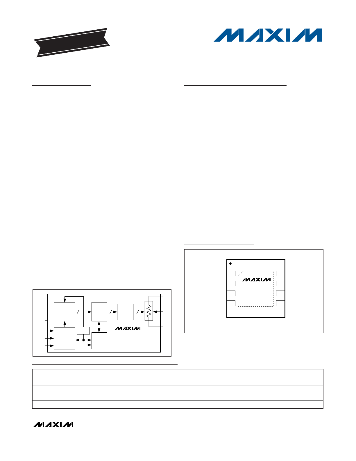
Pin Configuration
W
L
SPI
INTERFACE
256POSITION
DECODER
V
DD
GND
SCLK
8-BIT
NV
MEMORY
8-BIT
LATCH
8-BIT
SHIFT
REGISTER
POR
H
8
8
256
DIN
CS
MAX5422
MAX5423
MAX5424
Functional Diagram
SPI is a trademark of Motorola, Inc.
*EP = Exposed pad.
TOP VIEW
V
1
DD
SCLK
2
DIN
3
CS
45
MAX5422
MAX5423
MAX5424
H
8
W
7
6
L
GND
TDFN (3mm x 3mm)
PART TEMP RANGE
MAX5422ETA -40°C to +85°C50
MAX5423ETA -40°C to +85°C 100
MAX5424ETA -40°C to +85°C 200
END-TO-END
RESISTANCE (kΩ)
PIN-PACKAGE TOP MARK
8 TDFN-EP*
8 TDFN-EP*
8 TDFN-EP*
AIJ
AII
AIH
Page 2
MAX5422/MAX5423/MAX5424
256-Tap, Nonvolatile, SPI-Interface,
Digital Potentiometers
2 _______________________________________________________________________________________
ABSOLUTE MAXIMUM RATINGS
ELECTRICAL CHARACTERISTICS
(VDD= +2.7V to +5.25V, H = VDD, L = GND, TA= -40°C to +85°C. Typical values are at VDD= +5.0V, TA= +25°C, unless otherwise noted.)
Stresses beyond those listed under “Absolute Maximum Ratings” may cause permanent damage to the device. These are stress ratings only, and functional
operation of the device at these or any other conditions beyond those indicated in the operational sections of the specifications is not implied. Exposure to
absolute maximum rating conditions for extended periods may affect device reliability.
VDDto GND...........................................................-0.3V to +6.0V
All Other Pins to GND.................................-0.3V to (V
DD
+ 0.3V)
Maximum Continuous Current into H, L, and W
MAX5422......................................................................±1.3mA
MAX5423......................................................................±0.6mA
MAX5424......................................................................±0.3mA
Continuous Power Dissipation (T
A
= +70°C)
8-Pin TDFN (derate 24.4mW/°C above +70°C) .........1951mW
Operating Temperature Range ...........................-40°C to +85°C
Junction Temperature......................................................+150°C
Storage Temperature Range .............................-60°C to +150°C
Lead Temperature (soldering, 10s) .................................+300°C
PARAMETER SYMBOL CONDITIONS MIN TYP MAX UNITS
DC PERFORMANCE (VOLTAGE-DIVIDER MODE)
Resolution N 256 Taps
Integral Nonlinearity INL (Note 1) ±0.5 LSB
Differential Nonlinearity DNL (Note 1) ±0.5 LSB
End-to-End Resistance
Temperature Coefficient
Ratiometric Resistance
Temperature Coefficient
Zero-Scale Error
DC PERFORMANCE (VARIABLE-RESISTOR MODE)
Integral Nonlinearity
(Note 2)
Differential Nonlinearity
(Note 2)
DC PERFORMANCE (RESISTOR CHARACTERISTICS)
Wiper Resistance R
Wiper Capacitance C
TC
INL
DNL
W
W
R
MAX5422 -0.6
MAX5423 -0.3Full-Scale Error
MAX5424 -0.15
MAX5422 0.7
MAX5423 0.35
MAX5424 0.18
VDD = 3V ±3.0
V
= 5V ±1.5
DD
VDD = 3V, MAX5422, -40°C ≤ TA ≤ +85°C,
guaranteed monotonic
VDD = 3V, MAX5422, 0°C ≤ TA ≤ +85°C,
guaranteed monotonic
VDD = 3V, MAX5423 ±1.0
VDD = 3V, MAX5424 ±1.0
= 5V ±1.0
V
DD
VDD = 3V to 5.25V (Note 3) 325 675 Ω
MAX5422 37.5 50 62.5
MAX5423 75 100 125End-to-End Resistance
MAX5424 150 200 250
35 ppm/°C
5 ppm/°C
-1.0 +2.0
-1.0 +1.2
10 pF
LSB
LSB
LSB
LSB
kΩ
Page 3
MAX5422/MAX5423/MAX5424
256-Tap, Nonvolatile, SPI-Interface,
Digital Potentiometers
_______________________________________________________________________________________ 3
ELECTRICAL CHARACTERISTICS (continued)
(VDD= +2.7V to +5.25V, H = VDD, L = GND, TA= -40°C to +85°C. Typical values are at VDD= +5.0V, TA= +25°C, unless otherwise noted.)
TIMING CHARACTERISTICS
(VDD= +2.7V to +5.25V, H = VDD, L = GND, TA= -40°C to +85°C. Typical values are at VDD= +5.0V, TA= +25°C, unless otherwise
noted. See Figure 1.) (Note 7)
PARAMETER SYMBOL CONDITIONS MIN TYP MAX UNITS
DIGITAL INPUTS (CS, DIN, SCLK)
VDD = 3.4V to 5.25V 2.4
Input High Voltage (Note 4) V
Input Low Voltage V
Input Leakage Current I
Input Capacitance C
DYNAMIC CHARACTERISTICS
Wiper -3dB Bandwidth (Note 5)
NONVOLATILE MEMORY RELIABILITY
Data Retention TA = +85°C 50 Years
Endurance
POWER SUPPLY
Supply Voltage V
Standby Current I
Programming Current I
IN
DD
DD
PG
IH
VDD < 3.4V
VDD = 2.7V to 5.25V (Note 4) 0.8 V
IL
IN
MAX5422 100
MAX5423 50
MAX5424 25
TA = +25°C 200,000
T
= +85°C 50,000
A
Digital inputs = VDD or GND, TA = +25°C 0.5 1 µA
During nonvolatile write to memory; digital
inputs = V
or GND (Note 6)
DD
0.7 x
V
DD
±0.1 ±1 µA
5pF
2.70 5.25 V
200 400 µA
V
kHz
Stores
PARAMETER SYMBOL CONDITIONS MIN TYP MAX UNITS
ANALOG SECTION
MAX5422 400
ns
DIGITAL SECTION
SCLK Frequency f
SCLK Clock Period t
SCLK Pulse-Width High t
SCLK Pulse-Width Low t
CS Fall to SCLK Rise Setup t
SCLK Rise to CS Rise Hold t
DIN to SCLK Setup t
S
SCLK
CP
CH
CL
CSS
CSH
DS
MAX5423 600Wiper Settling Time (Note 8) t
MAX5424 1000
5MHz
200 ns
80 ns
80 ns
80 ns
0ns
50 ns
Page 4
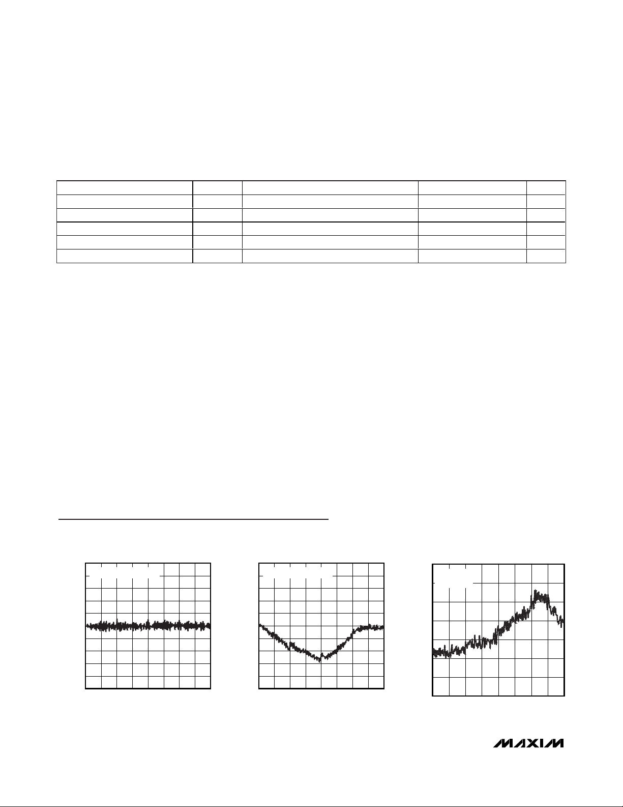
DNL vs. TAP POSITION
MAX5422 toc01
TAP POSITION
DNL (LSB)
224192128 16064 9632
-0.20
-0.15
-0.10
-0.05
0
0.05
0.10
0.15
0.20
0.25
-0.25
0256
VOLTAGE-DIVIDER MODE
INL vs. TAP POSITION
MAX5422 toc02
TAP POSITION
INL (LSB)
224192128 16064 9632
-0.20
-0.15
-0.10
-0.05
0
0.05
0.10
0.15
0.20
0.25
-0.25
0256
VOLTAGE-DIVIDER MODE
RESISTANCE (Ω)
100
200
300
400
500
600
700
0
WIPER RESISTANCE vs. TAP POSITION
MAX5422 toc03
TAP POSITION
224192128 16064 96320 256
VDD = 2.7V
I
SRC
= 50μA
Typical Operating Characteristics
(VDD= 5.0V, TA= +25°C, unless otherwise noted.)
MAX5422/MAX5423/MAX5424
256-Tap, Nonvolatile, SPI-Interface,
Digital Potentiometers
4 _______________________________________________________________________________________
TIMING CHARACTERISTICS (continued)
(VDD= +2.7V to +5.25V, H = VDD, L = GND, TA= -40°C to +85°C. Typical values are at VDD= +5.0V, TA= +25°C, unless otherwise
noted. See Figure 1.) (Note 7)
Note 1: The DNL and INL are measured with the potentiometer configured as a voltage-divider with H = VDDand L = GND. The
wiper terminal is unloaded and measured with a high-input-impedance voltmeter.
Note 2: The DNL and INL are measured with the potentiometer configured as a variable resistor. H is unconnected and L = GND.
For the 5V condition, the wiper terminal is driven with a source current of 80µA for the 50kΩ configuration, 40µA for the
100kΩ configuration, and 20µA for the 200kΩ configuration. For the 3V condition, the wiper terminal is driven with a source
current of 40µA for the 50kΩ configuration, 20µA for the 100kΩ, and 10µA for the 200kΩ configuration.
Note 3: The wiper resistance is measured using the source currents given in Note 2. For operation to V
DD
= 2.7V, see Maximum
Wiper Resistance vs. Temperature in the Typical Operating Characteristics.
Note 4: The device draws higher supply current when the digital inputs are driven with voltages between (V
DD
- 0.5V) and (GND +
0.5V). See Supply Current vs. Digital Input Voltage in the Typical Operating Characteristics.
Note 5: Wiper at midscale with a 10pF load (DC measurement). L = GND; an AC source is applied to H; and the W output is mea-
sured. A 3dB bandwidth occurs when the AC W/H value is 3dB lower than the DC W/H value.
Note 6: The programming current operates only during power-up and NV writes.
Note 7: Digital timing is guaranteed by design and characterization, and is not production tested.
Note 8: Wiper-settling time is the worst-case 0% to 50% rise-time measured between consecutive wiper positions. H = V
DD
, L =
GND, and the wiper terminal is unloaded and measured with a 10pF oscilloscope probe.
PARAMETER SYMBOL CONDITIONS MIN TYP MAX UNITS
DIN Hold after SCLK t
SCLK Rise to CS Fall Delay t
CS Rise to SCLK Rise Hold t
CS Pulse-Width High t
Write NV Register Busy Time t
DH
CS0
CS1
CSW
BUSY
0ns
20 ns
80 ns
200 ns
12 ms
Page 5

MAX5422/MAX5423/MAX5424
256-Tap, Nonvolatile, SPI-Interface,
Digital Potentiometers
_______________________________________________________________________________________ 5
Typical Operating Characteristics (continued)
(VDD= 5.0V, TA= +25°C, unless otherwise noted.)
THD+N RESPONSE
MAX5422 toc09
FREQUENCY (Hz)
THD+N (%)
10k1k100
0.001
0.01
0.1
1
10
100
0.0001
10 100k
1:1 RATIO
20Hz TO 20kHz BANDPASS
INL vs. TAP POSITION
(MAX5422)
MAX5422 toc10
TAP POSITION
INL (LSB)
224192160128966432
-0.5
0
0.5
1.0
1.5
2.0
-1.0
0256
VARIABLE-RESISTOR MODE
V
DD
= 2.7V
I
SRC
= 50μA
WIPER TRANSIENT AT POWER-ON
4μs/div
MAX5422 toc04
CL = 10pF
TAP = 128
H = V
DD
V
DD
1V/div
W
1V/div
END-TO-END RESISTANCE % CHANGE
MAXIMUM WIPER RESISTANCE
vs. TEMPERATURE
700
600
VDD = 2.7V
500
VDD = 3.0V
400
VDD = 4.5V
300
RESISTANCE (Ω)
200
VDD = 5.25V
100
0
-40 85
TEMPERATURE (°C)
END-TO-END RESISTANCE %
CHANGE vs. TEMPERATURE
1.0
0.8
0.6
0.4
0.2
0
-0.2
-0.4
-0.6
-0.8
-1.0
-40 10-15 356085
TEMPERATURE (°C)
600
MAX5422 toc07
603510-15
500
400
300
200
SUPPLY CURRENT (µA)
100
0
05
1.0
0.9
MAX5422toc05
0.8
0.7
0.6
0.5
0.4
0.3
SUPPLY CURRENT (μA)
0.2
0.1
SUPPLY CURRENT
vs. DIGITAL INPUT VOLTAGE
DIGITAL INPUT VOLTAGE (V)
STANDBY SUPPLY CURRENT
vs. TEMPERATURE
VDD = 5.25V
VDD = 4.0V
VDD = 3.0V
0
-40 85
TEMPERATURE (°C)
MAX5422 toc08
3421
VDD = 2.7V
603510-15
MAX5422 toc06
Page 6

MAX5422/MAX5423/MAX5424
256-Tap, Nonvolatile, SPI-Interface,
Digital Potentiometers
6 _______________________________________________________________________________________
Typical Operating Characteristics (continued)
(VDD= 5.0V, TA= +25°C, unless otherwise noted.)
INL vs. TAP POSITION
(MAX5423)
MAX5422 toc11
TAP POSITION
INL (LSB)
224192160128966432
-0.5
0
0.5
1.0
1.5
2.0
-1.0
0 256
VARIABLE-RESISTOR MODE
V
DD
= 2.7V
I
SRC
= 20μA
INL vs. TAP POSITION
(MAX5424)
2.0
VARIABLE-RESISTOR MODE
= 2.7V
V
DD
1.5
= 10μA
I
SRC
1.0
0.5
INL (LSB)
0
-0.5
-1.0
0256
TAP POSITION
DNL vs. TAP POSITION
(MAX5423)
0.3
VARIABLE-RESISTOR MODE
0.2
0.1
0
DNL (LSB)
-0.1
-0.2
-0.3
0256
TAP POSITION
MAX5422 toc14
224192160128966432
MAX5422 toc12
224192160128966432
0.5
VARIABLE-RESISTOR MODE
0.4
0.3
0.2
0.1
DNL (LSB)
0
-0.1
-0.2
-0.3
DNL vs. TAP POSITION
(MAX5422)
0.3
VARIABLE-RESISTOR MODE
0.2
0.1
0
DNL (LSB)
-0.1
-0.2
-0.3
0256
TAP POSITION
MAX5422 toc13
224192160128966432
DNL vs. TAP POSITION
(MAX5424)
MAX5422 toc15
2241921601289664320 256
TAP POSITION
Page 7

Detailed Description
The MAX5422/MAX5423/MAX5424 contain a resistor
array with 255 resistive elements. The MAX5422 has a
total end-to-end resistance of 50kΩ; the MAX5423 has
an end-to-end resistance of 100kΩ; and the MAX5424
has an end-to-end resistance of 200kΩ. The
MAX5422/MAX5423/MAX5424 allow access to the high,
low, and wiper terminals for a standard voltage-divider
configuration. H, L, and W can be connected in any
desired configuration as long as their voltages fall
between GND and VDD.
A simple, 3-wire, SPI serial interface moves the wiper
among the 256 tap points. The nonvolatile memory
stores the wiper position and recalls the stored wiper
position upon power-up. The nonvolatile memory is
guaranteed for 50 years for wiper data retention and up
to 200,000 wiper store cycles.
Analog Circuitry
The MAX5422/MAX5423/MAX5424 consist of a resistor
array with 255 resistive elements; 256 tap points are
accessible to the wiper, W, along the resistor string
between H and L. Select the wiper tap point by programming the potentiometer through the 3-wire (SPI)
interface. Eight data bits, and a control byte program
the wiper position. The H and L terminals of the
MAX5422/MAX5423/MAX5424 are similar to the two
end terminals of a mechanical potentiometer. The
MAX5422/MAX5423/MAX5424 feature power-on reset
circuitry that loads the wiper position from the nonvolatile memory at power-up.
Digital Interface
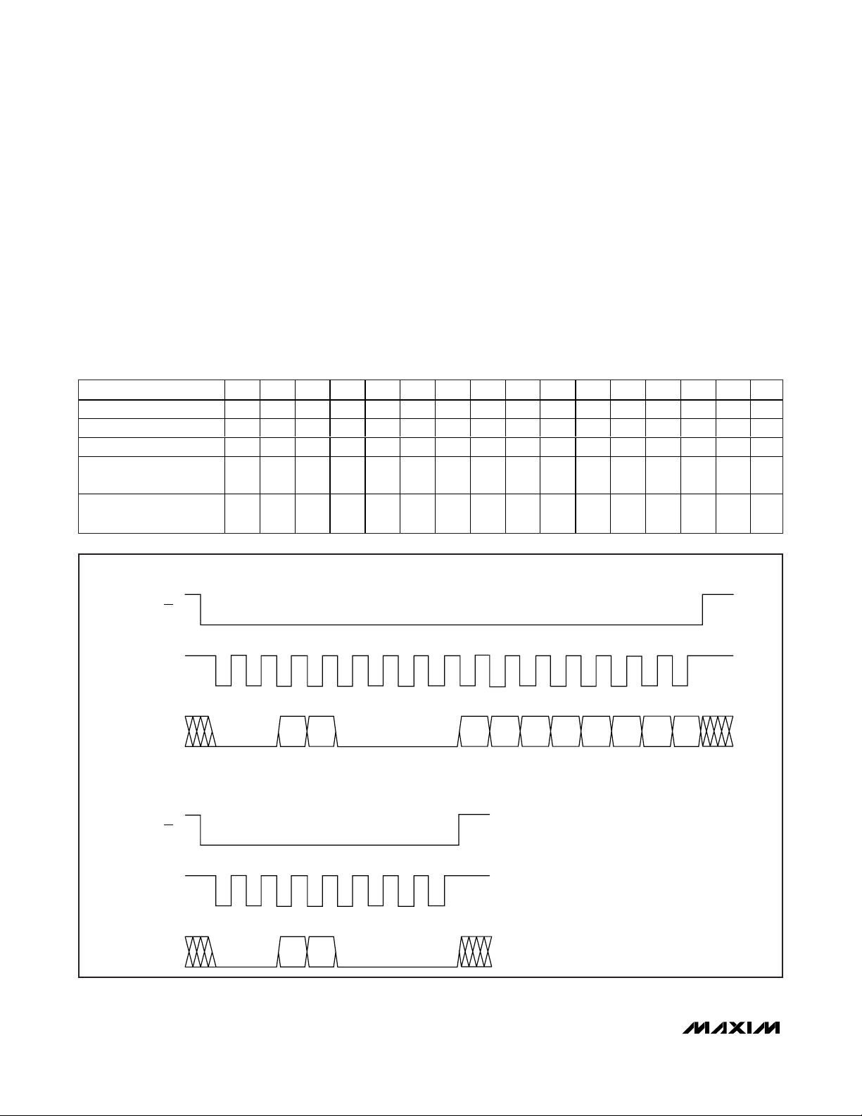
The MAX5422/MAX5423/MAX5424 use a 3-wire, SPIcompatible, serial data interface (Figure 1 and 2). This
write-only interface contains three inputs: chip-select
MAX5422/MAX5423/MAX5424
256-Tap, Nonvolatile, SPI-Interface,
Digital Potentiometers
_______________________________________________________________________________________ 7
Pin Description
Figure 1. Digital Interface and Timing Diagram
PIN NAME FUNCTION
1VDDPower-Supply Input. Bypass VDD with a 0.1µF capacitor from VDD to GND.
2 SCLK Serial-Interface Clock Input
3 DIN Serial-Interface Data Input
4 CS Active-Low Digital-Input Chip Select
5 GND Ground
6L
7 W Wiper Terminal
8H
— EP Exposed Pad. The exposed pad is not internally connected. Connect to GND or leave floating.
CS
SCLK
Low Terminal. The voltage at L can be greater than or less than the voltage at H. Current can flow into or
out of L.
High Terminal. The voltage at H can be greater than or less than the voltage at L. Current can flow into or
out of H.
t
t
CS0
t
CSS
t
t
CL
CH
t
CP
t
CSH
CSW
t
CS1
t
DS
DIN
t
DH
Page 8
MAX5422/MAX5423/MAX5424
(CS), data clock (SCLK), and data in (DIN). Drive CS
low to enable the serial interface and clock data synchronously into the shift register on each SCLK rising
edge.
The WRITE commands (C1, C0 = 00 or 01) require 16
clock cycles to clock in the command and data (Figure
2a). The COPY commands (C1, C0 = 10, 11) can use
either eight clock cycles to transfer the command bits
(Figure 2b) or 16 clock cycles with 8 data bits that are
disregarded by the device (Figure 2a).
After loading data into the shift register, drive CS high
to latch the data into the appropriate potentiometer
control register and disable the serial interface. Keep
CS low during the entire serial-data stream to avoid
corruption of the data.
The serial-data timing for the potentiometer is shown in
Figures 1 and 2.
256-Tap, Nonvolatile, SPI-Interface,
Digital Potentiometers
8 _______________________________________________________________________________________
Table 1. Register Map
Figure 2. Digital-Interface Format
CLOCK EDGE 1 2 3 4 5 6 7 8 9 10 11 12 13 14 15 16
Bit name — — C1 C0 — — — — D7 D6 D5 D4 D3 D2 D1 D0
Write wiper register 0 0 0 0 0 0 0 0 D7 D6 D5 D4 D3 D2 D1 D0
Write NV register 0 0 0 1 0 0 0 0 D7 D6 D5 D4 D3 D2 D1 D0
Copy wiper register to NV
register
Copy NV register to wiper
register
A) 16-BIT COMMAND/DATA WORD
CS
00100000————————
00110000————————
SCLK
1 2 3 4 5 6 7 8 9 10111213141516
DIN
B) 8-BIT COMMAND WORD
CS
SCLK
12345678
DIN
C1 C0
D7 D6 D5 D4 D3 D2 D1 D0C1 C0
Page 9

Write Wiper Register
Data written to this register (C1, C0 = 00) controls the
wiper positions. The 8 data bits (D7 to D0) indicate the
position of the wiper. For example, if DIN = 0000 0000,
the wiper moves to the position closest to L. If DIN =
1111 1111, the wiper moves closest to H.
This command writes data to the volatile random
access memory (RAM), leaving the NV registers
unchanged. When the device powers up, the data
stored in the NV registers transfers to the volatile wiper
register, moving the wiper to the stored position.
Write NV Register
The “write NV register” command (C1, C0 = 01) stores
the position of the wipers to the NV registers for use at
power-up. Alternatively, the “copy wiper register to NV
register” command writes to the NV register. Writing to the
NV registers, does not affect the position of the wipers.
Copy Wiper Register to NV Register
The “copy wiper register to NV register” command (C1,
C0 = 10) stores the current position of the wiper to the
NV register for use at power-up.
Copy NV Register to Wiper Register
The “copy NV register to wiper register” (C1, C0 = 11)
restores the wiper position to the current value stored in
the NV register.
Standby Mode
The MAX5422/MAX5423/MAX5424 feature a low-power
standby mode. When the device is not being pro-
grammed, it enters into standby mode and supply current drops to 0.5µA (typ).
Nonvolatile Memory
The internal EEPROM consists of a nonvolatile register
that retains the last value stored prior to power-down.
The nonvolatile register is programmed to midscale at
the factory. The nonvolatile memory is guaranteed for
50 years for wiper data retention and up to 200,000
wiper write cycles.
Power-Up
Upon power-up, the MAX5422/MAX5423/MAX5424
load the data stored in the nonvolatile wiper register
into the volatile wiper register, updating the wiper position with the data stored in the nonvolatile wiper register. This initialization period takes 10µs.
Applications Information
The MAX5422/MAX5423/MAX5424 are intended for circuits requiring digitally controlled adjustable resistance, such as LCD contrast control (where voltage
biasing adjusts the display contrast), or programmable
filters with adjustable gain and/or cutoff frequency.
Positive LCD Bias Control
Figures 3 and 4 show an application where a voltagedivider or variable resistor is used to make an
adjustable, positive LCD-bias voltage. The op amp provides buffering and gain to the resistor-divider network
made by the potentiometer (Figure 3) or to a fixed
resistor and a variable resistor (see Figure 4).
MAX5422/MAX5423/MAX5424
256-Tap, Nonvolatile, SPI-Interface,
Digital Potentiometers
_______________________________________________________________________________________ 9
Figure 3. Positive LCD-Bias Control Using a Voltage-Divider
Figure 4. Positive LCD-Bias Control Using a Variable Resistor
5V
H
MAX5422
MAX5423
MAX5424
W
L
30V
V
OUT
5V
30V
V
H
MAX5422
MAX5423
MAX5424
W
L
OUT
Page 10

MAX5422/MAX5423/MAX5424
Programmable Filter
Figure 5 shows the configuration for a 1st-order programmable filter. The gain of the filter is adjusted by
R2, and the cutoff frequency is adjusted by R3. Use the
following equations to calculate the DC gain (G) and
the 3dB cutoff frequency (fC):
Adjustable Voltage Reference
Figure 6 shows the MAX5422/MAX5423/MAX5424 used
as the feedback resistors in an adjustable voltage-reference application. Independently adjust the output
voltage of the MAX6160 from 1.23V to V
IN
- 0.2V by
changing the wiper position of the MAX5422/
MAX5423/MAX5424.
Offset Voltage and Gain Adjustment
Connect the high and low terminals of one potentiometer of a MAX5422/MAX5423/MAX5424 between the
NULL inputs of a MAX410 and the wiper to the op
amp’s positive supply to nullify the offset voltage over
the operating temperature range. Install another
MAX5422/MAX5423/MAX5424 potentiometer in the
feedback path to adjust the gain of the MAX410 (see
Figure 7).
256-Tap, Nonvolatile, SPI-Interface,
Digital Potentiometers
10 ______________________________________________________________________________________
Figure 5. Programmable Filter
Figure 6. Adjustable Voltage Reference
Figure 7. Offset Voltage Adjustment Circuit
Chip Information
TRANSISTOR COUNT: 10,191
PROCESS: BiCMOS
R
G
=+
f
=
C
1
1
R
2
1
RC
π× ×
23
C
V
IN
V
H
R3
MAX5422
MAX5423
MAX5424
W
L
H
R2
L
R1
W
OUT
5V
MAX5422
7
1
2
8
MAX410
3
4
-5V
6
+5V
V
IN
OUT
MAX6160
ADJ
V0 = 1.23V
R
V0 = 1.23V
R
V0 = 1.23V
R
GND
50kΩ
FOR THE MAX5422
(kΩ)
2
100kΩ
FOR THE MAX5423
(kΩ)
2
200kΩ
FOR THE MAX5424
(kΩ)
2
MAX5422
MAX5423
MAX5424
V0 REF
H
W
L
Page 11
MAX5422/MAX5423/MAX5424
256-Tap, Nonvolatile, SPI-Interface,
Digital Potentiometers
Maxim cannot assume responsibility for use of any circuitry other than circuitry entirely embodied in a Maxim product. No circuit patent licenses are
implied. Maxim reserves the right to change the circuitry and specifications without notice at any time.
Maxim Integrated Products, 120 San Gabriel Drive, Sunnyvale, CA 94086 408-737-7600 ____________________ 11
© 2004 Maxim Integrated Products Printed USA is a registered trademark of Maxim Integrated Products.
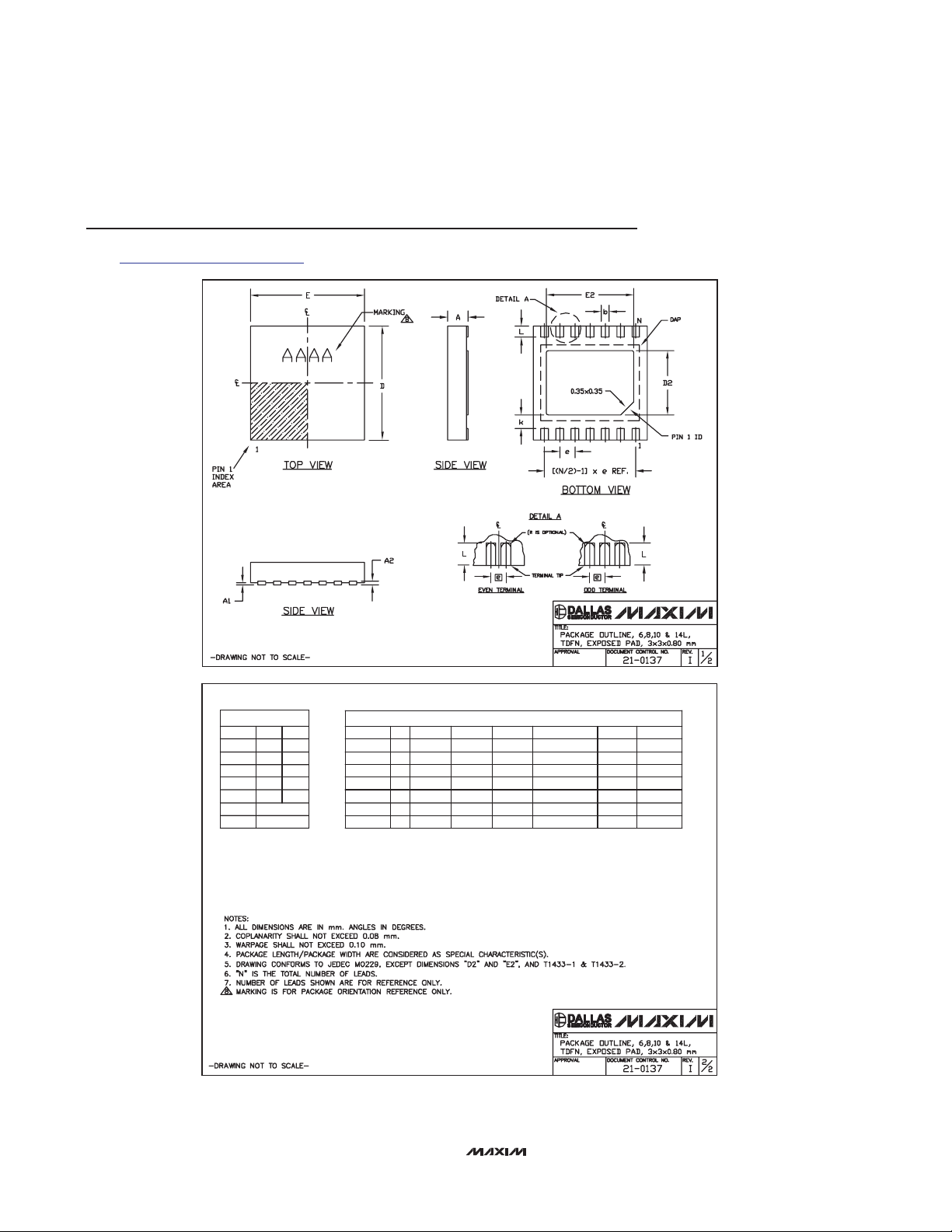
Package Information
(The package drawing(s) in this data sheet may not reflect the most current specifications. For the latest package outline information,
go to www.maxim-ic.com/packages
.)
6, 8, &10L, DFN THIN.EPS
COMMON DIMENSIONS
SYMBOL MIN. MAX.
A 0.70 0.80
D 2.90 3.10
E 2.90 3.10
A1
0.00 0.05
L 0.20 0.40
0.25 MIN.k
A2 0.20 REF.
PACKAGE VARIATIONS
PKG. CODE N D2 E2 e JEDEC SPEC b
T633-2 6 1.50±0.10 2.30±0.10 0.95 BSC MO229 / WEEA 0.40±0.05 1.90 REF
T833-2 8 1.50±0.10 2.30±0.10 0.65 BSC MO229 / WEEC 0.30±0.05 1.95 REF
T833-3 8 1.50±0.10 2.30±0.10 0.65 BSC MO229 / WEEC 0.30±0.05 1.95 REF
1.50±0.10 MO229 / WEED-3
2.30±0.10 MO229 / WEED-3 2.00 REF0.25±0.050.50 BSC1.50±0.1010T1033-2
0.40 BSC - - - - 0.20±0.05 2.40 REFT1433-2 14 2.30±0.101.70±0.10
[(N/2)-1] x e
2.00 REF0.25±0.050.50 BSC2.30±0.1010T1033-1
2.40 REF0.20±0.05- - - - 0.40 BSC1.70±0.10 2.30±0.1014T1433-1
 Loading...