

Page 1
19-3185; Rev 2; 8/04
________________________________
MAX5417/MAX5418/MAX5419
是非易失、线性数字电位
概述
器,与机械电位器功能相似,但可通过简单的2线数字接
口控制,允许多个器件进行通信。每个器件具有分离电
位器或可变电阻的功能,具有
这些器件内置非易失
EEPROM
上电时进行初始化处理。快速模式
400kbps
的通信速率,在许多应用场合可有效减小电路板
个抽头点。
256
,用于存储滑动端的位置,
TM
兼容接口允许
I2C
面积,简化电路连接。每个器件有一个工厂预置地址,
有四种地址选择(见
选择指南
,配合地址选择输入,共
)
提供八个唯一的地址组合。
MAX5417/MAX5418/MAX5419
(MAX5417)、100kΩ (MAX5418)和200kΩ (MAX5419)
标称电阻的端到端温度系数为
为
5ppm/°C
,非常适合低温漂可变电阻的应用,如低漂移、
提供了三个标称阻值:
35ppm/°C,
比率温度系数仅
50kΩ
。
可编程增益放大器。
MAX5417/MAX5418/MAX5419
封装,工作在
TDFN
-40°C至+85°C
采用
3mmx 3mm、8
扩展级温度范围。
________________________________
引脚
应用
替代机械电位器
低漂移可编程增益放大器
音量控制
液晶显示屏
(LCD)
对比度控制
256
抽头、非易失、
I2C
接口
数字电位器
________________________________
上电后从非易失存储器调用滑动端位置
♦
微型
♦
♦
♦
♦
♦
♦ 500nA (
♦
♦ 256
♦
♦
3mm x 3mm、8
端到端电阻温度系数:
比率温度系数:
阻值:
50kΩ/100kΩ/200kΩ
快速
兼容串行接口
I2C
典型值)静态电流
单电源
+2.7V至+5.25V
抽头
分压模式下
分压模式下
DNL
INL为:±0.5 LSB
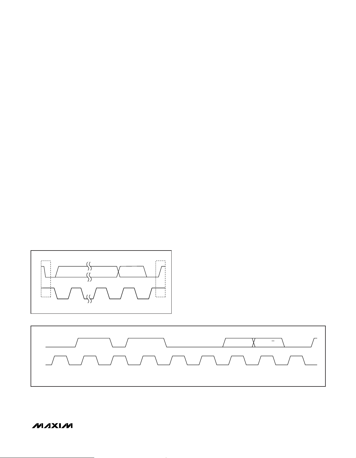
______________________________
定义的
8-BIT
SHIFT
REGISTER
I2C
INTERFACE
Philips I2C
标准规范的系统。
I2C
V
DD
GND
SDA
SCL
A
0
I2C是Philips Corp.
购买
Maxim Integrated Products, Inc.
产品,即得到了
Philips
引脚
TDFN
封装
35ppm/°C
5ppm/°C
供电
为:
±0.5 LSB
8
8-BIT
LATCH
POR
8-BIT
NV
MEMORY
的一个商标。
的专利许可、将这些产品用于符合
256-
8
POSITION
DECODER
MAX5417
MAX5418
MAX5419
或其从属授权公司的
功能图
256
特性
MAX5417/MAX5418/MAX5419
H
W
L
I2C
___________________________________________________________
PART TEMP RANGE I2C ADDRESS R (kΩ) PIN-PACKAGE TOP MARK
MAX5417LETA -40°C to +85°C 010100A
MAX5417META* -40°C to +85°C 010101A
MAX5417NETA* -40°C to +85°C 010110A
MAX5417PETA* -40°C to +85°C 010111A
MAX5418LETA -40°C to +85°C 010100A
MAX5418META* -40°C to +85°C 010101A
MAX5418NETA* -40°C to +85°C 010110A
MAX5418PETA* -40°C to +85°C 010111A
MAX5419LETA -40°C to +85°C 010100A
MAX5419META* -40°C to +85°C 010101A
MAX5419NETA* -40°C to +85°C 010110A
MAX5419PETA* -40°C to +85°C 010111A
*Future product—contact factory for availability.
**Exposed pad.
________________________________________________________________ Maxim Integrated Products 1
本文是
翻译错误,如需确认任何词语的准确性,请参考
索取免费样品和最新版的数据资料,请访问
正式英文资料的译文,
Maxim
不对翻译中存在的差异或由此产生的错误负责。请注意译文中可能存在文字组织或
Maxim
Maxim
提供的英文版资料。
Maxim
的主页:
0
0
0
0
0
0
0
0
0
0
0
0
引脚配置见本文的最后部分。
www.maxim-ic.com.cn
50 8 TDFN-EP** AIB
50 8 TDFN-EP** ALS
50 8 TDFN-EP** ALT
50 8 TDFN-EP** ALU
100 8 TDFN-EP** AIC
100 8 TDFN-EP** ALV
100 8 TDFN-EP** ALW
100 8 TDFN-EP** ALX
200 8 TDFN-EP** AID
200 8 TDFN-EP** ALY
200 8 TDFN-EP** ALZ
200 8 TDFN-EP** AMA
。
定购信息/选择指南
Page 2
256
抽头、非易失、
I2C
接口
数字电位器
ABSOLUTE MAXIMUM RATINGS
VDDto GND...........................................................-0.3V to +6.0V
All Other Pins to GND.................................-0.3V to (V
Maximum Continuous Current into H, L, and W
MAX5417......................................................................±1.3mA
MAX5418......................................................................±0.6mA
MAX5419......................................................................±0.3mA
Stresses beyond those listed under “Absolute Maximum Ratings” may cause permanent damage to the device. These are stress ratings only, and functional
operation of the device at these or any other conditions beyond those indicated in the operational sections of the specifications is not implied. Exposure to
absolute maximum rating conditions for extended periods may affect device reliability.
DD
+ 0.3V)
Continuous Power Dissipation (T
8-Pin TDFN (derate 24.4mW/°C above +70°C) .........1951mW
Operating Temperature Range ...........................-40°C to +85°C
Junction Temperature......................................................+150°C
Storage Temperature Range .............................-60°C to +150°C
Lead Temperature (soldering, 10s) .................................+300°C
ELECTRICAL CHARACTERISTICS
(VDD= +2.7V to +5.25V, H = VDD, L = GND, TA= -40°C to +85°C, unless otherwise noted. Typical values are at VDD= +5V, TA= +25°C.)
PARAMETER SYMBOL CONDITIONS MIN TYP MAX UNITS
DC PERFORMANCE (VOLTAGE-DIVIDER MODE)
Resolution 256 Taps
Integral Nonlinearity INL (Note 1) ±0.5 LSB
Differential Nonlinearity DNL (Note 1) ±0.5 LSB
End-to-End Temperature
Coefficient
Ratiometric Temperature
Coefficient
MAX5417/MAX5418/MAX5419
Zero-Scale Error
DC PERFORMANCE (VARIABLE-RESISTOR MODE)
Integral Nonlinearity
(Note 2)
Differential Nonlinearity
(Note 2)
DC PERFORMANCE (RESISTOR CHARACTERISTICS)
Wiper Resistance R
Wiper Capacitance C
TC
INL
DNL
W
W
HL
R
MAX5417_, 50Ω -0.6
MAX5418_, 100kΩ -0.3Full-Scale Error
MAX5419_, 200kΩ -0.15
MAX5417_, 50kΩ 0.6
MAX5418_, 100kΩ 0.3
MAX5419_, 200kΩ 0.15
V
= 3V ±3
DD
V
= 5V ±1.5
DD
V
= 3V, MAX5417_, 50kΩ,
DD
guaranteed monotonic
VDD = 3V, MAX5418_, 100kΩ ±1
MAX5419_, 200kΩ ±1
V
= 5V ±1
DD
VDD = 3V to 5.25V (Note 3) 325 675 Ω
MAX5417_ 37.5 50 62.5
MAX5418_ 75 100 125End-to-End Resistance R
MAX5419_ 150 200 250
-1 +2
= +70°C)
A
35 ppm/°C
5 ppm/°C
10 pF
LSB
LSB
LSB
LSB
kΩ
2 _______________________________________________________________________________________
Page 3
256
抽头、非易失、
I2C
接口
数字电位器
MAX5417/MAX5418/MAX5419
ELECTRICAL CHARACTERISTICS (continued)
(VDD= +2.7V to +5.25V, H = VDD, L = GND, TA= -40°C to +85°C, unless otherwise noted. Typical values are at VDD= +5V, TA= +25°C.)
PARAMETER SYMBOL CONDITIONS MIN TYP MAX UNITS
DIGITAL INPUTS
Input High Voltage (Note 4) V
Input Low Voltage V
Low-Level Output Voltage V
Input Leakage Current I
Input Capacitance 5pF
DYNAMIC CHARACTERISTICS
NONVOLATILE MEMORY
Data Retention TA = +85°C 50 Years
Endurance
POWER SUPPLY
Power-Supply Voltage V
Standby Current I
Programming Current
LEAK
DD
DD
VDD = 3.4V to 5.25V 2.4
IH
VDD < 3.4V 0.7 x V
V
IL
OL
= 2.7V to 5.25V (Note 4) 0.8 V
DD
3mA sink current 0.4 V
MAX5417_ 100
MAX5418_ 50Wiper -3dB Bandwidth (Note 5)
MAX5419_ 25
TA = +25°C 200,000
= +85°C 50,000
T
A
Digital inputs = V
= +25°C
T
A
During nonvolatile write;
digital inputs = V
or GND,
DD
or GND (Note 6)
DD
DD
2.70 5.25 V
0.5 1 µA
200 400 µA
V
±1 µA
kHz
Stores
TIMING CHARACTERISTICS
(VDD= +2.7V to +5.25V, H = VDD, L = GND, TA= -40°C to +85°C, unless otherwise noted. Typical values are at VDD= +5V, TA=
+25°C. See Figures 1 and 2.) (Note 7)
PARAMETER SYMBOL CONDITIONS MIN TYP MAX UNITS
ANALOG SECTION
MAX5417_ 500
ns
DIGITAL SECTION
SCL Clock Frequency f
Setup Time for START Condition t
Hold Time for START Condition t
CLK High Time t
CLK Low Time t
_______________________________________________________________________________________ 3
IL
SCL
SU-STA
HD-STA
HIGH
LOW
MAX5418_ 600Wiper Settling Time (Note 8) t
MAX5419_ 1000
400 kHz
0.6 µs
0.6 µs
0.6 µs
1.3 µs
Page 4
256
抽头、非易失、
I2C
接口
数字电位器
TIMING CHARACTERISTICS (continued)
(VDD= +2.7V to +5.25V, H = VDD, L = GND, TA= -40°C to +85°C, unless otherwise noted. Typical values are at VDD= +5V, TA=
+25°C. See Figures 1 and 2.) (Note 7)
PARAMETER SYMBOL CONDITIONS MIN TYP MAX UNITS
Data Setup Time t
Data Hold Time t
SDA, SCL Rise Time t
SDA, SCL Fall Time t
Setup Time for STOP Condition t
Bus Free Time Between STOP
and START Condition
Pulse Width of Spike Suppressed t
Maximum Capacitive Load for
Each Bus Line
Write NV Register Busy Time t
Note 1: The DNL and INL are measured with the potentiometer configured as a voltage-divider with H = VDDand L = GND. The
Note 2: The DNL and INL are measured with the potentiometer configured as a variable resistor. H is unconnected and L = GND.
Note 3: The wiper resistance is measured using the source currents given in Note 2. For operation to V
Note 4: The device draws higher supply current when the digital inputs are driven with voltages between (V
MAX5417/MAX5418/MAX5419
Note 5: Wiper at midscale with a 10pF load (DC measurement). L = GND; an AC source is applied to H; and the W output is mea-
Note 6: The programming current operates only during power-up and NV writes.
Note 7: SCL clock period includes rise and fall times t
Note 8: Wiper settling time is the worst-case 0% to 50% rise time measured between consecutive wiper positions. H = VDD,
Note 9: An appropriate bus pullup resistance must be selected depending on board capacitance. Refer to the document linked to
Note 10: The idle time begins from the initiation of the stop pulse.
wiper terminal is unloaded and measured with a high-input-impedance voltmeter.
For the 5V condition, the wiper terminal is driven with a source current of 80µA for the 50kΩ configuration, 40µA for the
100kΩ configuration, and 20µA for the 200kΩ configuration. For the 3V condition, the wiper terminal is driven with a source
current of 40µA for the 50kΩ configuration, 20µA for the 100kΩ configuration, and 10µA for the 200kΩ configuration.
Resistance vs. Temperature in the Typical Operating Characteristics.
0.5V). See Supply Current vs. Digital Input Voltage in the Typical Operating Characteristics.
sured. A 3dB bandwidth occurs when the AC W/H value is 3dB lower than the DC W/H value.
from a voltage level of (V
L = GND, and the wiper terminal is unloaded and measured with a 10pF oscilloscope probe (see the Typical Operating
Characteristics for the tap-to-tap switching transient).
this web address: www.semiconductors.philips.com/acrobat/literature/9398/39340011.pdf.
SU-DAT
HD-DAT
SU-STO
+ VIH) / 2.
IL
R
F
t
BUF
SP
C
B
BUSY
Minimum power-up rate = 0.2V/ms 1.3 µs
(Note 9) 400 pF
(Note 10) 12 ms
and tF. All digital input signals are specified with tR= tF= 2ns and timed
R
100 ns
0 0.9 µs
300 ns
300 ns
0.6 µs
50 ns
= 2.7V, see Wiper
DD
- 0.5V) and (GND +
DD
4 _______________________________________________________________________________________
Page 5
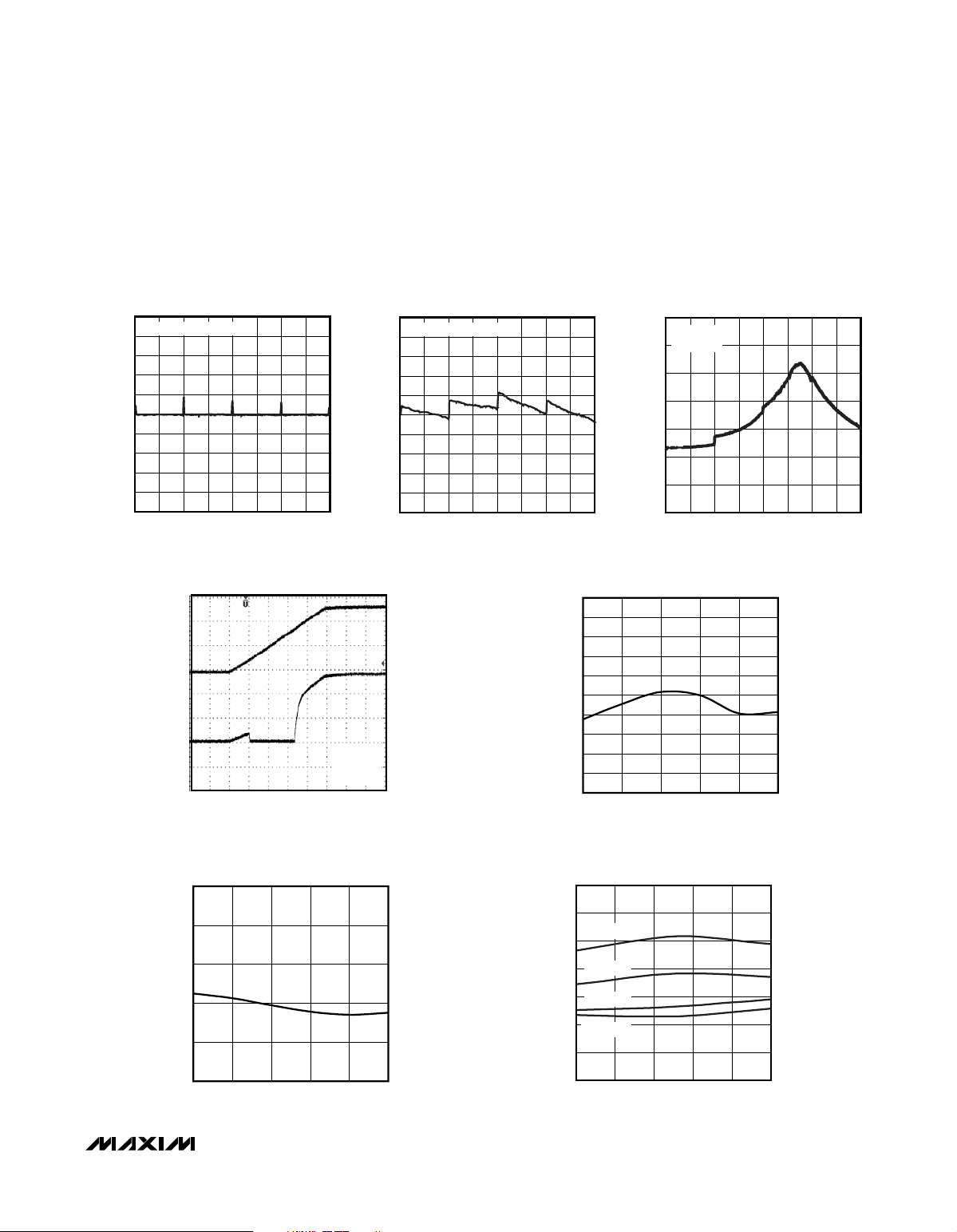
WIPER TRANSIENT AT POWER-ON
MAX5417 toc04
W
1V/div
V
DD
2V/div
4µs/div
CL = 10pF
TAP = 128
H = V
DD
END-TO-END RESISTANCE % CHANGE
vs. TEMPERATURE
MAX5417 toc05
TEMPERATURE (°C)
END-TO-END RESISTANCE % CHANGE
603510-15
-0.8
-0.6
-0.4
-0.2
0
0.2
0.4
0.6
0.8
1.0
-1.0
-40 85
DNL vs. TAP POSITION
MAX5417 toc01
TAP POSITION
RESISTANCE DNL (LSB)
224192160128966432
-0.20
-0.15
-0.10
-0.05
0
0.10
0.20
0.05
0.15
0.25
-0.25
0256
VOLTAGE-DIVIDER MODE
TAP POSITION
RESISTANCE INL (LSB)
224192160128966432
-0.20
-0.15
-0.10
-0.05
0
0.10
0.20
0.05
0.15
0.25
-0.25
0 256
INL vs. TAP POSITION
MAX5417 toc02
VOLTAGE-DIVIDER MODE
WIPER RESISTANCE vs. TAP POSITION
MAX5417 toc03
TAP POSITION
RESISTANCE (Ω)
224192160128966432
100
200
300
400
500
600
700
0
0 256
VDD = 2.7V
I
SRC
= 50µA
STANDBY SUPPLY CURRENT
vs. TEMPERATURE
MAX5417 toc06
TEMPERATURE (°C)
STANDBY SUPPLY CURRENT (µA)
603510-15
0.2
0.4
0.6
0.8
1.0
0
-40 85
WIPER RESISTANCE vs. TEMPERATURE
MAX5417 toc07
TEMPERATURE (°C)
RESISTANCE (Ω)
603510-15
100
200
300
400
500
600
700
0
-40 85
VDD = 2.7V
VDD = 3.0V
VDD = 4.5V
VDD = 5.25V
256
抽头、非易失、
数字电位器
_______________________________________________________________
(VDD= +5V, TA= +25°C, unless otherwise noted.)
I2C
接口
典型工作特性
MAX5417/MAX5418/MAX5419
_______________________________________________________________________________________ 5
Page 6
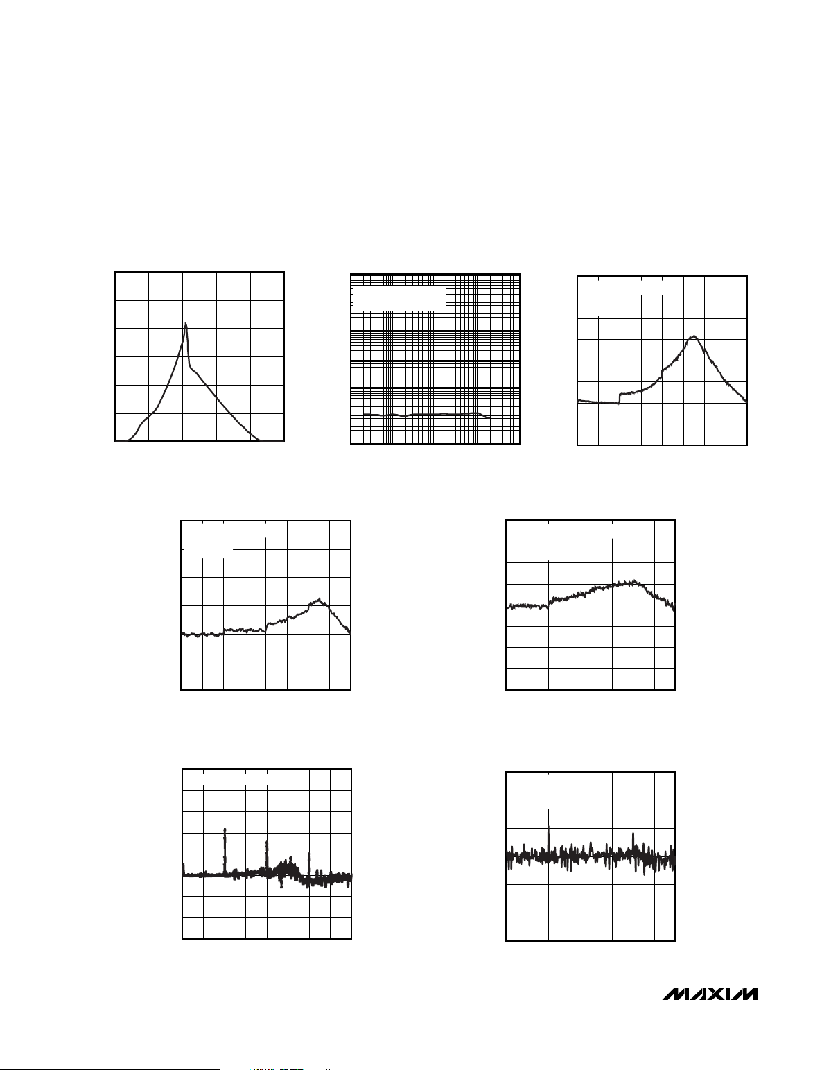
SUPPLY CURRENT
vs. DIGITAL INPUT VOLTAGE
MAX5417 toc08
DIGITAL INPUT VOLTAGE (V)
SUPPLY CURRENT (µA)
4321
100
200
300
400
500
600
0
05
10k1k100
0.001
0.01
0.1
1
10
100
0.0001
10 100k
THD+N RESPONSE
MAX5417 toc09
FREQUENCY (Hz)
THD+N (%)
1:1 RATIO
20Hz TO 20kHz BANDPASS
INL vs. TAP POSITION
(MAX5417)
MAX5417 toc10
TAP POSITION
RESISTANCE INL (LSB)
224192160128966432
-0.5
0
0.5
1.0
1.5
2.0
2.5
3.0
-1.0
0256
VARIABLE-RESISTOR MODE
V
DD
= 2.7V
I
SRC
= 50µA
256
抽头、非易失、
数字电位器
I2C
接口
___________________________________________________________
(VDD= +5V, TA= +25°C, unless otherwise noted.)
INL vs. TAP POSITION
(MAX5418)
2.0
VARIABLE-RESISTOR MODE
= 2.7V
V
DD
1.5
= 20µA
I
SRC
1.0
MAX5417/MAX5418/MAX5419
0.5
INL (LSB)
0
-0.5
-1.0
0256
TAP POSITION
MAX5417 toc11
224192160128966432
1.00
0.75
0.50
0.25
0
INL (LSB)
-0.25
-0.50
-0.75
-1.00
INL vs. TAP POSITION
VARIABLE-RESISTOR MODE
= 2.7V
V
DD
= 10µA
I
SRC
0256
(MAX5419)
TAP POSITION
典型工作特性(续
MAX5417 toc12
22419232 64 96 128 160
)
DNL vs. TAP POSITION
(MAX5417)
0.5
VARIABLE-RESISTOR MODE
0.4
0.3
6 _______________________________________________________________________________________
0.2
0.1
DNL (LSB)
0
-0.1
-0.2
-0.3
0256
TAP POSITION
DNL vs. TAP POSITION
(MAX5418)
0.3
VARIABLE-RESISTOR MODE
= 2.7V
V
DD
MAX5417 toc13
224192160128966432
0.2
= 20µA
I
SRC
0.1
0
DNL (LSB)
-0.1
-0.2
-0.3
0 256
TAP POSITION
MAX5417 toc14
224192160128966432
Page 7
256
抽头、非易失、
___________________________________________________________
(VDD= +5V, TA= +25°C, unless otherwise noted.)
I2C
接口
数字电位器
典型工作特性(续
MAX5417/MAX5418/MAX5419
)
0.3
VARIABLE-RESISTOR MODE
V
DD
0.2
I
SRC
0.1
0
DNL (LSB)
-0.1
-0.2
-0.3
DNL vs. TAP POSITION
(MAX5419)
= 2.7V
= 10µA
TAP POSITION
MAX5417 toc15
22419232 64 96 128 1600 256
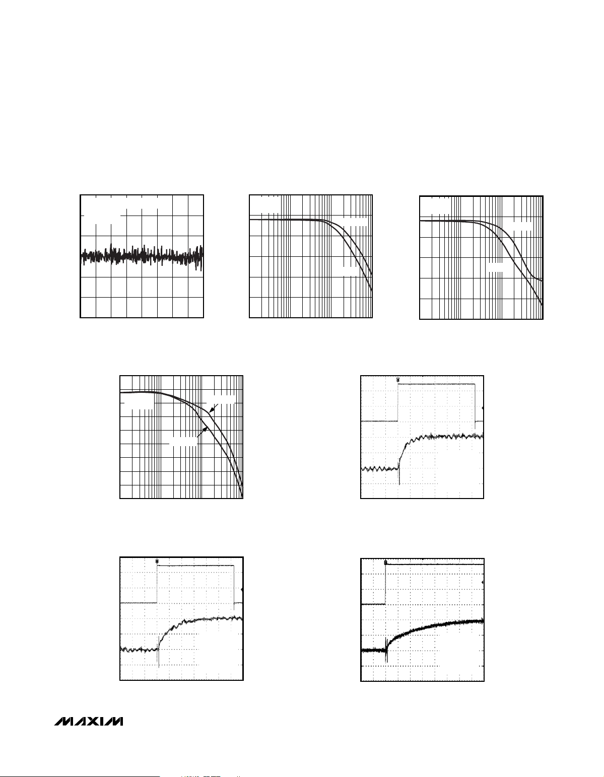
MIDSCALE WIPER RESPONSE vs. FREQUENCY
(MAX5419)
0
-5
MAX5419
-10
TAP = 128
-15
-20
-25
-30
WIPER RESPONSE (dB)
-35
-40
-45
1 1000
CL = 50pF
FREQUENCY (kHz)
CL = 10pF
10010
MIDSCALE WIPER RESPONSE vs. FREQUENCY
MIDSCALE WIPER RESPONSE vs. FREQUENCY
(MAX5417)
0
MAX5417
TAP = 128
-5
-10
-15
-20
WIPER RESPONSE (dB)
-25
-30
11000
FREQUENCY (kHz)
CL = 10pF
CL = 50pF
10010
MAX5417 toc16
0
MAX5418
TAP = 128
-5
-10
-15
-20
WIPER RESPONSE (dB)
-25
-30
1 1000
TAP-TO-TAP SWITCHING TRANSIENT
(MAX5417)
MAX5417 toc18
MAX5417
C
L
FROM TAP 127
TO TAP 128
H = V
1µs/div
(MAX5418)
FREQUENCY (kHz)
MAX5417 toc19
= 10pF
DD
CL = 50pF
10010
SDA
2V/div
W
10mV/div
CL = 10pF
MAX5417 toc17
TAP-TO-TAP SWITCHING TRANSIENT
(MAX5418)
1µs/div
MAX5417 toc20
MAX5418
= 10pF
C
L
FROM TAP 127
TO TAP 128
H = V
DD
SDA
2V/div
W
10mV/div
TAP-TO-TAP SWITCHING TRANSIENT
(MAX5419)
1µs/div
MAX5417 toc21
MAX5419
= 10pF
C
L
FROM TAP 127
TO TAP 128
H = V
DD
SDA
2V/div
W
10mV/div
_______________________________________________________________________________________ 7
Page 8
256
抽头、非易失、
数字电位器
I2C
接口
___________________________________________________________________
功能
电容旁路
t
HD-STA
至
GND
。
t
SU-STO
V
DD
t
SU-DAT
名称
t
LOW
t
HD-STA
电源输入,电压范围:
接口时钟输入
I2C
接口数据输入
I2C
地址输入端,设置器件ID的A0位。
地
低端
滑动端
高端
裸露焊盘
t
HIGH
t
R
t
F
2.7V至5.25V。用0.1µF
t
HD-DAT
t
SU-STA
引脚
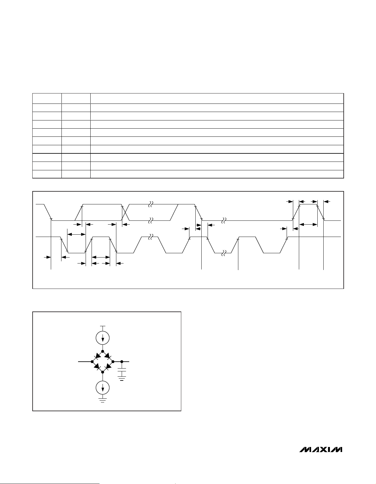
PIN NAME FUNCTION
1VDDPower-Supply Input. 2.7V to 5.25V voltage range. Bypass with a 0.1µF capacitor from VDD to GND.
2 SCL I2C-Interface Clock Input
3 SDA I2C-Interface Data Input
4 A0 Address Input. Sets the A0 bit in the device ID address.
5 GND Ground
6 L Low Terminal
7 W Wiper Terminal
8 H High Terminal
— EP Exposed Pad
SDA
SCL
MAX5417/MAX5418/MAX5419
S Sr A
PARAMETERS ARE MEASURED FROM 30% TO 70%.
引脚说明
t
R
PS
t
F
t
BUF
图
1. I2C
串行接口时序
____________________________
V
DD
I
= 3mA
OL
MAX5417/MAX5418/MAX5419
个电阻单元。
端到端阻值为
MAX5417
100kΩ,MAX5417
端到端阻值为
MAX5417/MAX5418/MAX5419
SDA
V
OUT
400pF
= 0mA
I
OH
动端可以构成标准的分压器,H、L和W端可以任意配置,
只需保证各端电压在
简单的2线
I2C
GND和V
兼容串行接口可以在
动端。非易失存储器储存并在上电时恢复滑动端的位置。
非易失存储器确保
200,000
持50年。
图
负载电路
2.
8 _______________________________________________________________________________________
内置电阻阵列,包含
端到端阻值为
通过连接高端、低端和滑
之间。
DD
次抽头读写,寄存器数据可保
详细说明
50kΩ,MAX5418
200kΩ
个触点间调节滑
256
255
。
Page 9
模拟电路
MAX5417/MAX5418/MAX5419
个电阻单元;
255
串接至滑动端
口对数字电位器编程实现。8位数据,一个地址字节,和
一个控制字节设置抽头位置。
MAX5419的H、L
MAX5417/MAX5418/MAX5419
电时从非易失存储器自动装载滑动端的位置。
个抽头点可以沿着H、L之间的电阻
256
。滑动端的位置选择通过2线
(W)
端与机械电位器的两个端点相同。
内置一个电阻阵列,包含
接
(I2C)
MAX5417/MAX5418/
带有上电复位电路,在上
数字接口
MAX5417/MAX5418/MAX5419
用于存储滑动端的位置,以便上电时的初始化处理。移
位寄存器对控制位和地址位进行解码,将数据写入适当
的数据寄存器。数据可以写入易失存储寄存器,立即更
新滑动端的位置,也可以写入非易失寄存器存储。
易失寄存器在系统加电期间能够保持数据。一旦系统断
电,易失寄存器的内容被清除。非易失寄存器在系统断
电时仍能保存数据。一旦上电,上电复位电路将非易失
存储器的内容自动传送到易失寄存器中,更新滑动端的
位置。
内置非易失
EEPROM
256
抽头、非易失、
I2C
数字电位器
MAX5417/MAX5418/MAX5419
TM
SMBus
(SDA)
主设备通常是微控制器,启动
MAX5419
传输(见图1)。
MAX5417/MAX5418/MAX5419的SDA
开路输出,
MAX5417/MAX5418/MAX5419的SCL
若2线接口挂接有多个主机,或者是具有
出的单主机系统,
,
阻。
每次数据传输先由主机发送启动
然后发送
8位(图4),1
停止
接口不工作时
始数据传输,即
降沿。当主机完成与从机的通信后发送停止条件,即在
SCL
总线,进行另外的传输(图3)。
兼容的2线接口接收数据,该接口采用串行数据线
和串行时钟线
的全部数据传输,并产生
线上需要一个典型值为
SDA
SCL
MAX5417/MAX5418/MAX5419的7
个命令字节(图7)和1个数据字节,最后是
(STOP)
为高电平时
条件
(P) (图3)
SCL和SDA
SCL
SDA
实现主、从设备之间的通信。
(SCL)
线上需接典型值为
。
均为高。主机发送启动条件开
为高电平时
出现由低至高的上升沿。然后释放
作为从设备从
MAX5417/MAX5418/
时钟,同步数据
SCL
可作为输入或漏极
4.7kΩ
只能作为输入端。
SCL
4.7kΩ
(START)
条件
启动条件和停止条件
出现由高至低的下
SDA
接口
串行寻址
或
I2C
的上拉电阻。
漏极开路输
的上拉电
(S) (图3)
位从地址和第
MAX5417/MAX5418/MAX5419
,
SDA
SCL
S
START
CONDITION
图
启动条件和停止条件
3.
SDA
SCL
*See the Ordering Information/Selector Guide section for other address options.
图
4.
SMBus是Intel Corporation
01
MSB LSB
从地址
的一个商标。
_______________________________________________________________________________________ 9
0 1 0* 0*
P
STOP
CONDITION
每个时钟传输一个数据位。
需保持稳定(图5)。
A0
为高时,
SCL
NOP/W ACK
上的数据必
SDA
位传输
Page 10
256
抽头、非易失、
数字电位器
I2C
接口
表1.
应答位是第9个时钟位,它是收到每个数据字节的应答握
手信号(图6)。因此,每个字节的有效传输需要9位。主
机产生第9个时钟脉冲,接收端在应答时钟周期内将
低电平。当主机向
据时,
为它们是数据的接收者。
MAX5417/MAX5418/MAX5419
PART SUFFIX A6 A5 A4 A3 A2 A1 A0 NOP/W
L 0 1 0 1 0 0 0 NOP/W
L 0 1 0 1 0 0 1 NOP/W
M 0 1 0 1 0 1 0 NOP/W
M 0 1 0 1 0 1 1 NOP/W
N 0 1 0 1 1 0 0 NOP/W
N 0 1 0 1 1 0 1 NOP/W
P 0 1 0 1 1 1 0 NOP/W
P 0 1 0 1 1 1 1 NOP/W
拉低,所以,在时钟为高电平期间
SDA
MAX5417/MAX5418/MAX5419
MAX5417/MAX5418/MAX5419
产生应答信号,因
必须稳定在
SDA
的地址码
ADDRESS BYTE
应答信号
传输数
MAX5417/MAX5418/MAX5419
MAX5417/MAX5418/MAX5419
接下来的2位由工厂设置(见表1)。将A0输入接
,可以在两个唯一地址中为器件选择做出选择。只
V
DD
有具有唯一地址的器件才能共享总线。因此,最多可以
有8个
线上。
从地址
MAX5417/MAX5418/MAX5419
MAX5417/MAX5418/MAX5419
紧随7位从地址的第8位是
示写操作,置高表示空操作。
具有7位从地址(图4)。
NOP/W
位,
NOP/W
位置低表
提供四种从地址(表1)。
的高4位地址始终为
MAX5417/MAX5418/MAX5419
0101
或
GND
挂接在同一总
,
SCL
SDA
图
START
CONDITION
应答信号
6.
1
289
NOT ACKNOWLEDGE
ACKNOWLEDGE
SDA
SCL
DATA STABLE,
DATA VALID
图
位传输
5.
10 ______________________________________________________________________________________
CHANGE OF
DATA ALLOWED
CLOCK PULSE FOR
ACKNOWLEDGMENT
Page 11

256
抽头、非易失、
数字电位器
I2C
接口
MAX5417/MAX5418/MAX5419
CONTROL BYTE IS STORED ON RECEIPT OF STOP CONDITION
S A0SLAVE ADDRESS CONTROL BYTE
图
接收到的命令字节
7.
HOW CONTROL BYTE AND DATA BYTE MAP INTO
MAX5417/MAX5418/MAX5419 REGISTERS
ACKNOWLEDGE FROM
MAX5417/MAX5418/MAX5419
S AA
NOP/W
图
接收到的命令和单个数据字节
8.
D15 D14 D13 D12 D11 D10 D9 D8
ACKNOWLEDGE FROM
MAX5417/MAX5418/MAX5419
AP
NOP/W
ACKNOWLEDGE FROM
MAX5417/MAX5418/MAX5419
D15 D14 D13 D12 D11 D10 D9 D8 D1 D0D3 D2D5 D4D7 D6
0SLAVE ADDRESS CONTROL BYTE DATA BYTE
ACKNOWLEDGE FROM
MAX5417/MAX5418/MAX5419
MAX5417/MAX5418/MAX5419
ACKNOWLEDGE FROM
1 BYTE
A
P
写数据格式
向
MAX5417/MAX5418/MAX5419
包括器件从地址字节(第8位置零)和至少一个字节的信息
。第1个信息字节为命令字节,命令字节之后是数
(图7)
据字节。第一个数据字节按照命令字节的选择写入内部
寄存器(图8)。
写入数据时,传输内容
命令字节
命令字节用于选择滑动端数据的源地址和目的地址(非易
失或易失存储寄存器),或在非易失或易失存储寄存器之
间交换数据(见表2)。
______________________________________________________________________________________ 11
:数据字节写入易失存储寄存器,滑动端位置更
VREG
新为易失存储寄存器中的数据。
NVREG
:数据字节写入非易失存储寄存器,滑动端位置
保持不变。
NVREGxVREG
:数据从非易失存储寄存器传送到易失
寄存器(滑动端位置更新)。
VREGxNVREG
:数据从易失寄存器传送到非易失存储
寄存器。
命令说明
Page 12

256
抽头、非易失、
数字电位器
表2. 命令字节
I2C
ADDRESS BYTE CONTROL BYTE DATA BYTE
接口
SCL CYCLE
NUMBER
VREG 0 1 0 1 A2 A1 A0 0 0 0 0 1 0 0 0 1 D7 D6 D5 D4 D3 D2 D1 D0
NVREG 0 1 0 1 A2 A1 A0 0 0 0 1 0 0 0 0 1 D7 D6 D5 D4 D3 D2 D1 D0
NVREGxVREG 0 1 0 1 A2 A1 A0 0 0 1 1 0 0 0 0 1 D7 D6 D5 D4 D3 D2 D1 D0
VREGxNVREG 0 1 0 1 A2 A1 A0 0 0 1 0 1 0 0 0 1 D7 D6 D5 D4 D3 D2 D1 D0
12345678 9 1011121314151617 18 19 2021 22 232425 26 27 P
S
A6 A5 A4 A3 A2 A1 A0 ACK
TX
NV V R3 R2 R1 R0 ACK D7 D6 D5 D4 D3 D2 D1 D0 ACK
非易失存储器
内置
EEPROM
写入的数据。非易失寄存器在工厂预置为零值。
上电时,
寄存器的数据装入易失寄存器内,并随之更新抽头位置。
初始化过程需要
MAX5417/MAX5418/MAX5419
件没有编程时,进入待机模式,电流消耗典型值为
。
500nA
MAX5417/MAX5418/MAX5419
____________________________
MAX5417/MAX5418/MAX5419
系统,如
度),可调增益和/或截止频率的可编程滤波器等。
包含一个8位非易失寄存器,保留断电前
MAX5417/MAX5418/MAX5419
。
10µs
将存储在非易失
具有低功耗待机模式。器
用于需要数控调节电阻的
对比度调节(利用偏置电压调节显示器对比
LCD
上电
待机
应用信息
图9和图10显示了用分压器或可变电阻调节
置电压的应用电路图。运放提供电阻分压电路的缓冲和
放大,电阻分压电路可以由电位器构成(图9),或由一个
固定电阻串联一个可变电阻构成(图
图11为一阶可编程滤波器电路。滤波器的增益由R2调节,
截止频率通过R3调节。利用下式计算增益
止频率
:
)
(f
C
1
R
1
=+
G
=
f
C
2
R
1
××
23π
RC
LCD
。
10)
可编程滤波器
正偏置控制
正向偏
LCD
(G)和3dB
截
5V
H
MAX5417
MAX5418
MAx5419
图
用分压器实现
9.
12 ______________________________________________________________________________________
LCD
W
L
正偏调节
30V
V
OUT
MAX5417
MAX5418
MAX5419
图
用可变电阻实现
10.
5V
H
L
LCD
W
正偏调节
30V
V
OUT
Page 13

图
11.
V
IN
H
MAX5417
MAX5418
MAX5419
可编程滤波器
256
抽头、非易失、
I2C
接口
数字电位器
MAX5417/MAX5418/MAX5419
W
L
R3
C
R1
H
R2
W
L
V
OUT
W
L
R2 R1
图
失调电压与增益调节电路
13.
5V
MAX5417
MAX5418
7
1
3
8
MAX410
2
4
-5V
H
MAX5419
6
+5V
V
图
12.
MAX5417
MAX5418
MAX5419
可调电压基准
MAX6160
V0 = 1.23V
R
V0 = 1.23V
R
V0 = 1.23V
R
IN
OUT
ADJ
GND
50kΩ
FOR THE MAX5417
(kΩ)
2
100kΩ
FOR THE MAX5418
(kΩ)
2
200kΩ
FOR THE MAX5419
(kΩ)
2
V0 REF
H
W
L
可调电压基准
图12所示为使用
多级可调电压基准应用中的反馈电阻。通过改变
MAX5418/MAX5419
VIN- 0.2V
的范围内独立调节
MAX5417/MAX5418/MAX5419
滑动端的位置,可在从
MAX6160
的输出电压。
作为
MAX5417/
至
1.23V
____________________________
TOP VIEW
V
SDA
1
DD
2
MAX5417
3
MAX5418
MAX5419
4
TDFN
87H
6
5
WSCL
L
GNDA0
失调电压和增益调节
将
MAX5417
的
NULL
度范围内调节失调电压。另一个电位器用在
馈回路上以调节其增益。
中一个电位器的高端和低端分别接
输入,滑动端接运放的正电源,可在整个工作温
____________________________
TRANSISTOR COUNT: 4637
PROCESS: BiCMOS
引脚配置
MAX410
MAX410
芯片信息
的反
______________________________________________________________________________________ 13
Page 14

256
抽头、非易失、
数字电位器
I2C
接口
___________________________________________________________________
(本数据资料提供的封装图可能不是最近的规格,如需最近的封装外型信息,请查询 www.maxim-ic.com.cn/packages。)
D
N
PIN 1
INDEX
AREA
E
DETAIL A
A
E2
C
L
L
e
C
L
L
e
封装信息
6, 8, &10L, DFN THIN.EPS
MAX5417/MAX5418/MAX5419
PACKAGE OUTLINE, 6, 8, 10 & 14L,
TDFN, EXPOSED PAD, 3x3x0.80 mm
NUMBER OF LEADS SHOWN ARE FOR REFERENCE ONLY
14 ______________________________________________________________________________________
21-0137
1
F
2
Page 15

256
抽头、非易失、
I2C
数字电位器
_______________________________________________________________
(本数据资料提供的封装图可能不是最近的规格,如需最近的封装外型信息,请查询 www.maxim-ic.com.cn/packages。)
封装信息(续
接口
MAX5417/MAX5418/MAX5419
)
COMMON DIMENSIONS
SYMBOL
A 0.70 0.80
D 2.90 3.10
E 2.90 3.10
A1 0.00 0.05
L
A2 0.20 REF.
PACKAGE VARIATIONS
PKG. CODE
T833-1
T1033-1
MIN. MAX.
0.25 MIN.k
0.40
1.50±0.10
1.50±0.10
1.70±0.10 2.30±0.1014T1433-1
1.70±0.10
2.30±0.101.50±0.106T633-1 0.95 BSC MO229 / WEEA 1.90 REF
2.30±0.108
2.30±0.1010
0.65 BSC
0.50 BSC
0.40 BSC
0.40 BSC
0.20
N D2 E2 e
JEDEC SPEC
MO229 / WEEC
MO229 / WEED-3
- - - - 0.20±0.03 2.40 REFT1433-2 14 2.30±0.10
b
0.40±0.05
[(N/2)-1] x e
1.95 REF0.30±0.05
2.00 REF0.25±0.05
2.40 REF0.20±0.03- - - -
PACKAGE OUTLINE, 6, 8, 10 & 14L,
TDFN, EXPOSED PAD, 3x3x0.80 mm
21-0137
2
F
2
MAXIM
北京
8328
免费电话:
电话:
010-6201 0598
传真:
010-6201 0298
Maxim不对Maxim
北京办事处
信箱 邮政编码
800 810 0310
产品以外的任何电路使用负责,也不提供其专利许可。
100083
保留在任何时间、没有任何通报的前提下修改产品资料和规格的权利。
Maxim
Maxim Integrated Products, 120 San Gabriel Drive, Sunnyvale, CA 94086 408-737-7600 ____________________ 15
© 2004 Maxim Integrated Products Printed USA
是
Maxim Integrated Products, Inc.
的注册商标。
Page 16

MAX5417, MAX5417L, MAX5417M, MAX5417N, MAX5417P, MAX5418, MAX5419 256抽头、非易失、 I²C接口数字电位器 - 概述
Temp.
ENGLISH • 简体中文 • 日本語 • 한국어
Login | Register
请输入关键词或器件型号
最新内容 产品 方案 设计 应用 技术支持 销售联络 公司简介 我的Maxim
Maxim > 产品 > 数字电位器(pot) > MAX5417, MAX5417L, MAX5417M, ...
MAX5417, MAX5417L, MAX5417M, MAX5417N, MAX5417P, MAX5418,
MAX5419
256抽头、非易失、 I²C 接口数字电位器
业内尺寸最小的256抽头电位器,3mm x 3mm TDFN 封装
概述 技术文档 定购信息 用户说明 (0) 所有内容
状况
状况:生产中。
概述
MAX5417/MAX5418/MAX5419为非易失性、线性变化的数字电位器,实现机械电
位器的功能,采用简单的2线数字接口就取代了机械调节,且允许控制多个器件。
每个器件具有分立电位器或可变电阻等相同功能,提供256级抽头。
完整的数据资料
提供更新的英文版数据资料
这些器件内置非易失性EEPROM,用来存储中心抽头的位置,以便在上电期间进
行初始化。快速模式的兼容I²C串行接口允许以400kbps的数据速率进行通讯,为
多数应用尽可能减小了电路板尺寸,简化了布线。每个器件提供四个工厂预置地
址之一(参阅完整数据资料中的选型指南),和一个地址输入端,以实现总共8个唯
一地址的组合。
MAX5417/MAX5418/MAX5419提供三种标称电阻值:50kΩ (MAX5417)、100kΩ (MAX5418)及200kΩ (MAX5419)。标称
端对端的电阻温度系数为50ppm/°C,比例系数仅5ppm/°C。以上特性使这些器件尤其适合于要求低温漂系数的可变电阻
应用,如可编程增益放大器电路结构。
MAX5417/MAX5418/MAX5419采用3mm x 3mm、8引脚TDFN封装,工作在-40°C至+85°C的扩展级工作范围内。
现备有评估板:MAX5417LEVCMODU, MAX5417LEVKIT
关键特性 应用/使用
上电时由非失性存储器设定中心抽头位置
微型3mm x 3mm、8引脚TDFN封装
35ppm/°C端到端电阻温度系数
5ppm/°C比例温度系数
50kΩ/100kΩ/200kΩ电阻值
快速的兼容I²C串行接口
500nA ( 典型值)的静态电源电流
单电源工作:+2.7V至+5.25V
256抽头位置
在分压器模式下,达到±0.5 LSB 的DNL
在分压器模式下,达到±0.5 LSB 的INL
可提供评估板
英文
中文
下载
Rev. 3 (PDF, 288kB)
下载
Rev. 2 (PDF, 536kB)
液晶显示器(LCD)对比度控制
低偏差可编程增益放大器
替代机械电位器
音量控制
Key Specifications: Digital Potentiometers
http://china.maxim-ic.com/datasheet/index.mvp/id/4205[2010-8-19 9:06:35]
Page 17

MAX5417, MAX5417L, MAX5417M, MAX5417N, MAX5417P, MAX5418, MAX5419 256抽头、非易失、 I²C接口数字电位器 - 概述
Smallest
R
Part
Number
Taper POTs
Control
Interface
Wiper
Memory
Steps
MAX5418
MAX5419 200
Linear 1
2-Wire
Serial
Non-
Volatile
256
END-
TO-END
(kΩ)
100
MAX5417 50
查看所有Digital Potentiometers (128)
图表
Coeff.
(ppm/
°C)
Wiper
Resistance
(Ω)
I
CC
Available Pckg.
@5V
(µA)
(mm
typ typ max max w/pins
50 325 1 9.6
2
)
See
Notes
$1.25
@1k
$1.25
@1k
$1.16
@5k
Price
功能框图
相关产品
MAX5417LEVCMODU,
MAX5417_、MAX5418_、MAX5419_评估板/评估系统
MAX5417LEVKIT
类似产品:浏览其它类似产品线
查看所有Digital Potentiometers (128产品)
更多信息
顶标 MAX5417L
顶标 MAX5417M
顶标 MAX5417N
顶标 MAX5417P
顶标 MAX5417L
顶标 MAX5417M
顶标 MAX5417N
顶标 MAX5417P
顶标 MAX5417L
顶标 MAX5417M
顶标 MAX5417N
顶标 MAX5417P
顶标 MAX5417L
顶标 MAX5417M
顶标 MAX5417N
http://china.maxim-ic.com/datasheet/index.mvp/id/4205[2010-8-19 9:06:35]
Page 18

MAX5417, MAX5417L, MAX5417M, MAX5417N, MAX5417P, MAX5418, MAX5419 256抽头、非易失、 I²C接口数字电位器 - 概述
MAX5417P
顶标
顶标 MAX5417L
顶标 MAX5417M
顶标 MAX5417N
顶标 MAX5417P
顶标 MAX5418L
顶标 MAX5418M
顶标 MAX5418N
顶标 MAX5418P
顶标 MAX5419L
顶标 MAX5419M
顶标 MAX5419N
顶标 MAX5419P
新品发布 [ 2004-03-29 (English only) ]
没有找到你需要的产品吗?
应用工程师帮助选型,下个工作日回复
参数搜索
应用帮助
概述 技术文档 定购信息
概述
关键特性
应用/使用
关键指标
图表
注释、注解
相关产品
联络我们:信息反馈、提出问题 • 对该网页的评价 • 发送本网页 • 隐私权政策 • 法律声明
© 2010 Maxim Integrated Products 版权所有
数据资料
应用笔记
评估板
设计指南
可靠性报告
软件/模型
参考文献: 19-3185 Rev. 3; 2009-04-24
本页最后一次更新: 2009-10-08
价格与供货
样品
在线订购
封装信息
无铅信息
http://china.maxim-ic.com/datasheet/index.mvp/id/4205[2010-8-19 9:06:35]
Page 19

General Description
The MAX5417/MAX5418/MAX5419 nonvolatile, lineartaper, digital potentiometers perform the function of a
mechanical potentiometer by replacing the mechanics
with a simple 2-wire digital interface, allowing communication with multiple devices. Each device performs the
same function as a discrete potentiometer or variable
resistor and has 256 tap points.
The devices feature an internal, nonvolatile EEPROM
used to store the wiper position for initialization during
power-up. The fast-mode I
2
C-compatible serial interface
allows communication at data rates up to 400kbps, minimizing board space and reducing interconnection complexity in many applications. Each device is available with
one of four factory-preset addresses (see the
Selector
Guide
) and features an address input for a total of eight
unique address combinations.
The MAX5417/MAX5418/MAX5419 provide three nomi-
nal resistance values: 50kΩ (MAX5417), 100kΩ
(MAX5418), or 200kΩ (MAX5419). The nominal resistor
temperature coefficient is 35ppm/°C end-to-end, and
only 5ppm/°C ratiometric. This makes the devices ideal
for applications requiring a low-temperature-coefficient
variable resistor, such as low-drift, programmable gainamplifier circuit configurations.
The MAX5417/MAX5418/MAX5419 are available in a
3mm x 3mm 8-pin TDFN package, and are specified
over the extended -40°C to +85°C temperature range.
Applications
Mechanical Potentiometer Replacement
Low-Drift Programmable-Gain Amplifiers
Volume Control
Liquid-Crystal Display (LCD) Contrast Control
Features
o Power-On Recall of Wiper Position from
Nonvolatile Memory
o Tiny 3mm x 3mm 8-Pin TDFN Package
o 35ppm/°C End-to-End Resistance Temperature
Coefficient
o 5ppm/°C Ratiometric Temperature Coefficient
o 50kΩ/100kΩ/200kΩ Resistor Values
o Fast I
2
C-Compatible Serial Interface
o 500nA (typ) Static Supply Current
o Single-Supply Operation: +2.7V to +5.25V
o 256 Tap Positions
o ±0.5 LSB DNL in Voltage-Divider Mode
o ±0.5 LSB INL in Voltage-Divider Mode
MAX5417/MAX5418/MAX5419
256-Tap, Nonvolatile, I2C-Interface,
Digital Potentiometers
________________________________________________________________
Maxim Integrated Products
1
Ordering Information/Selector Guide
Functional Diagram
19-3185; Rev 4; 4/10
For pricing, delivery, and ordering information, please contact Maxim Direct at 1-888-629-4642,
or visit Maxim’s website at www.maxim-ic.com.
Pin Configuration appears at end of data sheet.
+
Denotes a lead(Pb)-free/RoHS-compliant package.
**
Exposed pad.
V
GND
SDA
SCL
8-BIT
8
POR
8-BIT
LATCH
8-BIT
NV
MEMORY
DD
A
0
SHIFT
REGISTER
I2C
INTERFACE
256-
POSITION
DECODER
MAX5417
MAX5418
MAX5419
256
8
H
W
L
PART TEMP RANGE I2C ADDRESS R (kΩ) PIN-PACKAGE TOP MARK
MAX5417LETA+ -40°C to +85°C 010100A
MAX5417META+ -40°C to +85°C 010101A
MAX5417NETA+ -40°C to +85°C 010110A
MAX5417PETA+ -40°C to +85°C 010111A
MAX5418LETA+ -40°C to +85°C 010100A
MAX5418META+ -40°C to +85°C 010101A
MAX5418NETA+ -40°C to +85°C 010110A
MAX5418PETA+ -40°C to +85°C 010111A
MAX5419LETA+ -40°C to +85°C 010100A
MAX5419META+ -40°C to +85°C 010101A
MAX5419NETA+ -40°C to +85°C 010110A
MAX5419PETA+ -40°C to +85°C 010111A
0
0
0
0
0
0
0
0
0
0
0
0
50 8 TDFN-EP** AIB
50 8 TDFN-EP** ALS
50 8 TDFN-EP** ALT
50 8 TDFN-EP** ALU
100 8 TDFN-EP** AIC
100 8 TDFN-EP** ALV
100 8 TDFN-EP** ALW
100 8 TDFN-EP** ALX
200 8 TDFN-EP** AID
200 8 TDFN-EP** ALY
200 8 TDFN-EP** ALZ
200 8 TDFN-EP** AMA
Page 20

MAX5417/MAX5418/MAX5419
256-Tap, Nonvolatile, I2C-Interface,
Digital Potentiometers
2 _______________________________________________________________________________________
ABSOLUTE MAXIMUM RATINGS
ELECTRICAL CHARACTERISTICS
(VDD= +2.7V to +5.25V, H = VDD, L = GND, TA= -40°C to +85°C, unless otherwise noted. Typical values are at VDD= +5V, TA= +25°C.)
Stresses beyond those listed under “Absolute Maximum Ratings” may cause permanent damage to the device. These are stress ratings only, and functional
operation of the device at these or any other conditions beyond those indicated in the operational sections of the specifications is not implied. Exposure to
absolute maximum rating conditions for extended periods may affect device reliability.
VDDto GND...........................................................-0.3V to +6.0V
All Other Pins to GND.................................-0.3V to (V
DD
+ 0.3V)
Maximum Continuous Current into H, L, and W
MAX5417......................................................................±1.3mA
MAX5418......................................................................±0.6mA
MAX5419......................................................................±0.3mA
Continuous Power Dissipation (T
A
= +70°C)
8-Pin TDFN (derate 24.4mW/°C above +70°C) .........1951mW
Operating Temperature Range ...........................-40°C to +85°C
Junction Temperature......................................................+150°C
Storage Temperature Range .............................-60°C to +150°C
Lead Temperature (soldering, 10s) .................................+300°C
Soldering Temperature (reflow) .......................................+260°C
PARAMETER SYMBOL CONDITIONS MIN TYP MAX UNITS
DC PERFORMANCE (VOLTAGE-DIVIDER MODE)
Resolution 256 Taps
Integral Nonlinearity INL (Note 1) ±0.5 LSB
Differential Nonlinearity DNL (Note 1) ±0.5 LSB
End-to-End Temperature
Coefficient
Ratiometric Temperature
Coefficient
Zero-Scale Error
DC PERFORMANCE (VARIABLE-RESISTOR MODE)
Integral Nonlinearity
(Note 2)
Differential Nonlinearity
(Note 2)
DC PERFORMANCE (RESISTOR CHARACTERISTICS)
Wiper Resistance R
Wiper Capacitance C
End-to-End Resistance R
TC
INL
DNL
W
HL
R
MAX5417_, 50Ω -0.6
MAX5418_, 100kΩ -0.3Full-Scale Error
MAX5419_, 200kΩ -0.15
MAX5417_, 50kΩ 0.6
MAX5418_, 100kΩ 0.3
MAX5419_, 200kΩ 0.15
V
= 3V ±3
DD
V
= 5V ±1.5
DD
V
= 3V, MAX5417_, 50kΩ -1 +2
DD
VDD = 3V, MAX5418_, 100kΩ ±1
VDD = 3V, MAX5419_, 200kΩ ±1
V
= 5V ±1
DD
VDD = 3V to 5.25V (Note 3) 325 675 Ω
W
MAX5417_ 37.5 50 62.5
MAX5418_ 75 100 125
MAX5419_ 150 200 250
35 ppm/°C
5 ppm/°C
10 pF
LSB
LSB
LSB
LSB
kΩ
Page 21

MAX5417/MAX5418/MAX5419
256-Tap, Nonvolatile, I2C-Interface,
Digital Potentiometers
_______________________________________________________________________________________ 3
ELECTRICAL CHARACTERISTICS (continued)
(VDD= +2.7V to +5.25V, H = VDD, L = GND, TA= -40°C to +85°C, unless otherwise noted. Typical values are at VDD= +5V, TA= +25°C.)
TIMING CHARACTERISTICS
(VDD= +2.7V to +5.25V, H = VDD, L = GND, TA= -40°C to +85°C, unless otherwise noted. Typical values are at VDD= +5V, TA=
+25°C. See Figures 1 and 2.) (Note 7)
DIGITAL INPUTS
V
= 3.4V to 5.25V 2.4
Input High Voltage (Note 4) V
Input Low Voltage V
Low-Level Output Voltage V
Input Leakage Current I
Input Capacitance 5pF
DYNAMIC CHARACTERISTICS
Wiper -3dB Bandwidth (Note 5)
NONVOLATILE MEMORY
Data Retention TA = +85°C 50 Years
Endurance
POWER SUPPLY
Power-Supply Voltage V
Standby Current I
Programming Current
IH
IL
OL
LEAK
DD
DD
DD
VDD < 3.4V 0.7 x V
V
= 2.7V to 5.25V (Note 4) 0.8 V
DD
3mA sink current 0.4 V
MAX5417_ 100
MAX5418_ 50
MAX5419_ 25
TA = +25°C 200,000
T
= +85°C 50,000
A
Digital inputs = V
T
= +25°C
A
During nonvolatile write;
digital inputs = V
or GND,
DD
or GND (Note 6)
DD
DD
±1 µA
kHz
Stores
2.70 5.25 V
0.5 1 µA
200 400 µA
V
PARAMETER SYMBOL CONDITIONS MIN TYP MAX UNITS
ANALOG SECTION
MAX5417_ 500
ns
DIGITAL SECTION
SCL Clock Frequency f
Setup Time for START Condition t
Hold Time for START Condition t
CLK High Time t
CLK Low Time t
IL
SCL
SU-STA
HD-STA
HIGH
LOW
MAX5418_ 600Wiper Settling Time (Note 8) t
MAX5419_ 1000
400 kHz
0.6 µs
0.6 µs
0.6 µs
1.3 µs
Page 22

MAX5417/MAX5418/MAX5419
256-Tap, Nonvolatile, I2C-Interface,
Digital Potentiometers
4 _______________________________________________________________________________________
Note 1: The DNL and INL are measured with the potentiometer configured as a voltage-divider with H = VDDand L = GND. The
wiper terminal is unloaded and measured with a high-input-impedance voltmeter.
Note 2: The DNL and INL are measured with the potentiometer configured as a variable resistor. H is unconnected and L = GND.
For the 5V condition, the wiper terminal is driven with a source current of 80µA for the 50kΩ configuration, 40µA for the
100kΩ configuration, and 20µA for the 200kΩ configuration. For the 3V condition, the wiper terminal is driven with a source
current of 40µA for the 50kΩ configuration, 20µA for the 100kΩ configuration, and 10µA for the 200kΩ configuration.
Note 3: The wiper resistance is measured using the source currents given in Note 2. For operation to V
DD
= 2.7V, see Wiper
Resistance vs. Temperature in the
Typical Operating Characteristics.
Note 4: The device draws higher supply current when the digital inputs are driven with voltages between (VDD- 0.5V) and (GND +
0.5V). See Supply Current vs. Digital Input Voltage in the
Typical Operating Characteristics.
Note 5: Wiper at midscale with a 10pF load (DC measurement). L = GND; an AC source is applied to H; and the W output is mea-
sured. A 3dB bandwidth occurs when the AC W/H value is 3dB lower than the DC W/H value.
Note 6: The programming current operates only during power-up and NV writes.
Note 7: SCL clock period includes rise and fall times t
R
and tF. All digital input signals are specified with tR= tF= 2ns and timed
from a voltage level of (V
IL
+ VIH) / 2.
Note 8: Wiper settling time is the worst-case 0% to 50% rise time measured between consecutive wiper positions. H = V
DD
,
L = GND, and the wiper terminal is unloaded and measured with a 10pF oscilloscope probe (see the
Typical Operating
Characteristics
for the tap-to-tap switching transient).
Note 9: An appropriate bus pullup resistance must be selected depending on board capacitance. Refer to the document linked to
this web address: www.semiconductors.philips.com/acrobat/literature/9398/39340011.pdf.
Note 10: The idle time begins from the initiation of the stop pulse.
TIMING CHARACTERISTICS (continued)
(VDD= +2.7V to +5.25V, H = VDD, L = GND, TA= -40°C to +85°C, unless otherwise noted. Typical values are at VDD= +5V, TA=
+25°C. See Figures 1 and 2.) (Note 7)
PARAMETER SYMBOL CONDITIONS MIN TYP MAX UNITS
Data Setup Time t
Data Hold Time t
SDA, SCL Rise Time t
SDA, SCL Fall Time t
Setup Time for STOP Condition t
Bus Free Time Between STOP
and START Condition
Pulse Width of Spike Suppressed t
Maximum Capacitive Load for
Each Bus Line
Write NV Register Busy Time t
SU-DAT
HD-DAT
R
F
SU-STO
t
BUF
SP
C
BUSY
Minimum power-up rate = 0.2V/ms 1.3 µs
(Note 9) 400 pF
B
(Note 10) 12 ms
100 ns
0 0.9 µs
300 ns
300 ns
0.6 µs
50 ns
Page 23

MAX5417/MAX5418/MAX5419
256-Tap, Nonvolatile, I2C-Interface,
Digital Potentiometers
_______________________________________________________________________________________
5
Typical Operating Characteristics
(VDD= +5V, TA= +25°C, unless otherwise noted.)
STANDBY SUPPLY CURRENT
vs. TEMPERATURE
MAX5417 toc06
TEMPERATURE (°C)
STANDBY SUPPLY CURRENT (µA)
603510-15
0.2
0.4
0.6
0.8
1.0
0
-40 85
WIPER RESISTANCE vs. TEMPERATURE
MAX5417 toc07
TEMPERATURE (°C)
RESISTANCE (Ω)
603510-15
100
200
300
400
500
600
700
0
-40 85
VDD = 2.7V
VDD = 3.0V
VDD = 4.5V
VDD = 5.25V
DNL vs. TAP POSITION
0.25
VOLTAGE-DIVIDER MODE
0.20
0.15
0.10
0.05
0
-0.05
-0.10
RESISTANCE DNL (LSB)
-0.15
-0.20
-0.25
0 256
TAP POSITION
WIPER TRANSIENT AT POWER-ON
4µs/div
MAX5417 toc01
224192160128966432
MAX5417 toc04
CL = 10pF
TAP = 128
H = V
DD
0.25
VOLTAGE-DIVIDER MODE
0.20
0.15
0.10
0.05
0
-0.05
RESISTANCE INL (LSB)
-0.10
-0.15
-0.20
-0.25
0256
TAP POSITION
MAX5417 toc02
224192160128966432
END-TO-END RESISTANCE % CHANGE
INL vs. TAP POSITION
V
DD
2V/div
W
1V/div
1.0
0.8
0.6
0.4
0.2
0
-0.2
-0.4
-0.6
END-TO-END RESISTANCE % CHANGE
-0.8
-1.0
-40 85
WIPER RESISTANCE vs. TAP POSITION
700
VDD = 2.7V
= 50µA
I
SRC
600
500
400
300
RESISTANCE (Ω)
200
100
0
0256
vs. TEMPERATURE
TEMPERATURE (°C)
MAX5417 toc03
224192160128966432
TAP POSITION
MAX5417 toc05
603510-15
Page 24

MAX5417/MAX5418/MAX5419
256-Tap, Nonvolatile, I2C-Interface,
Digital Potentiometers
6 _______________________________________________________________________________________
Typical Operating Characteristics (continued)
(VDD= +5V, TA= +25°C, unless otherwise noted.)
SUPPLY CURRENT
600
500
400
300
200
SUPPLY CURRENT (µA)
100
0
05
DIGITAL INPUT VOLTAGE (V)
4321
MAX5417 toc08
100
1:1 RATIO
10
20Hz TO 20kHz BANDPASS
1
0.1
THD+N (%)
0.01
0.001
0.0001
10 100k
vs. DIGITAL INPUT VOLTAGE
THD+N RESPONSE
FREQUENCY (Hz)
INL vs. TAP POSITION
(MAX5418)
2.0
VARIABLE-RESISTOR MODE
= 2.7V
V
DD
1.5
= 20µA
I
SRC
1.0
0.5
INL (LSB)
0
-0.5
-1.0
0256
TAP POSITION
MAX5417 toc11
224192160128966432
INL vs. TAP POSITION
(MAX5417)
3.0
VARIABLE-RESISTOR MODE
2.5
= 2.7V
V
MAX5417 toc09
10k1k100
DD
= 50µA
I
SRC
2.0
1.5
1.0
0.5
RESISTANCE INL (LSB)
0
-0.5
-1.0
0256
TAP POSITION
MAX5417 toc10
224192160128966432
INL vs. TAP POSITION
(MAX5419)
1.00
VARIABLE-RESISTOR MODE
0.75
0.50
0.25
INL (LSB)
-0.25
-0.50
-0.75
-1.00
= 2.7V
V
DD
= 10µA
I
SRC
0
0256
TAP POSITION
MAX5417 toc12
22419232 64 96 128 160
DNL vs. TAP POSITION
(MAX5417)
0.5
VARIABLE-RESISTOR MODE
0.4
0.3
0.2
0.1
DNL (LSB)
0
-0.1
-0.2
-0.3
0256
TAP POSITION
MAX5417 toc13
224192160128966432
0.3
0.2
0.1
0
DNL (LSB)
-0.1
-0.2
-0.3
DNL vs. TAP POSITION
(MAX5418)
VARIABLE-RESISTOR MODE
= 2.7V
V
DD
= 20µA
I
SRC
0256
TAP POSITION
MAX5417 toc14
224192160128966432
Page 25

MAX5417/MAX5418/MAX5419
256-Tap, Nonvolatile, I2C-Interface,
Digital Potentiometers
_______________________________________________________________________________________
7
Typical Operating Characteristics (continued)
(VDD= +5V, TA= +25°C, unless otherwise noted.)
DNL vs. TAP POSITION
(MAX5419)
0.3
VARIABLE-RESISTOR MODE
= 2.7V
V
DD
0.2
0.1
0
DNL (LSB)
-0.1
-0.2
-0.3
I
SRC
= 10µA
TAP POSITION
MAX5417 toc15
WIPER RESPONSE (dB)
22419232 64 96 128 1600 256
MIDSCALE WIPER RESPONSE vs. FREQUENCY
(MAX5419)
0
-5
MAX5419
-10
TAP = 128
-15
-20
-25
-30
WIPER RESPONSE (dB)
-35
-40
-45
1 1000
CL = 50pF
FREQUENCY (kHz)
CL = 10pF
10010
MIDSCALE WIPER RESPONSE vs. FREQUENCY
(MAX5417)
0
MAX5417
TAP = 128
-5
-10
-15
-20
-25
-30
1 1000
FREQUENCY (kHz)
CL = 10pF
CL = 50pF
10010
TAP-TO-TAP SWITCHING TRANSIENT
MAX5417 toc18
MAX5417 toc16
MIDSCALE WIPER RESPONSE vs. FREQUENCY
(MAX5418)
0
MAX5418
TAP = 128
-5
-10
-15
-20
WIPER RESPONSE (dB)
-25
-30
1 1000
FREQUENCY (kHz)
(MAX5417)
1µs/div
MAX5417 toc19
MAX5417
= 10pF
C
L
FROM TAP 127
TO TAP 128
H = V
DD
CL = 50pF
10010
SDA
2V/div
W
10mV/div
CL = 10pF
MAX5417 toc17
TAP-TO-TAP SWITCHING TRANSIENT
(MAX5418)
1µs/div
MAX5417 toc20
MAX5418
= 10pF
C
L
FROM TAP 127
TO TAP 128
H = V
DD
SDA
2V/div
W
10mV/div
TAP-TO-TAP SWITCHING TRANSIENT
(MAX5419)
1µs/div
MAX5417 toc21
MAX5419
= 10pF
C
L
FROM TAP 127
TO TAP 128
H = V
DD
SDA
2V/div
W
10mV/div
Page 26

MAX5417/MAX5418/MAX5419
256-Tap, Nonvolatile, I2C-Interface,
Digital Potentiometers
8 _______________________________________________________________________________________
Pin Description
Detailed Description
The MAX5417/MAX5418/MAX5419 contain a resistor
array with 255 resistive elements. The MAX5417 has a
total end-to-end resistance of 50kΩ, the MAX5418 has
an end-to-end resistance of 100kΩ, and the MAX5419
has an end-to-end resistance of 200kΩ. The
MAX5417/MAX5418/MAX5419 allow access to the high,
low, and wiper terminals for a standard voltage-divider
configuration. H, L, and W can be connected in any
desired configuration as long as their voltages fall
between GND and V
DD
.
A simple 2-wire I2C-compatible serial interface moves
the wiper among the 256 tap points. A nonvolatile memory stores the wiper position and recalls the stored wiper
position in the nonvolatile memory upon power-up. The
nonvolatile memory is guaranteed for 50 years for wiper
data retention and up to 200,000 wiper store cycles.
Figure 1. I2C Serial-Interface Timing Diagram
Figure 2. Load Circuit
PIN NAME FUNCTION
1VDDPower-Supply Input. 2.7V to 5.25V voltage range. Bypass with a 0.1µF capacitor from VDD to GND.
2 SCL I2C-Interface Clock Input
3 SDA I2C-Interface Data Input
4A0Address Input. Sets the A0 bit in the device ID address.
5 GND Ground
6 L Low Terminal
7 W Wiper Terminal
8 H High Terminal
—EP
Exposed Pad. Internally connected to GND. Connect to a large ground plane to maximize thermal
performance. Not intended as an electrical point.
SDA
t
SU-DAT
t
LOW
SCL
t
t
HD-STA
S Sr A
PARAMETERS ARE MEASURED FROM 30% TO 70%.
HIGH
t
R
t
HD-DAT
t
F
t
SU-STA
V
DD
I
OL
= 3mA
SDA
V
OUT
400pF
I
= 0mA
OH
t
HD-STA
t
SU-STO
t
R
PS
t
F
t
BUF
Page 27

MAX5417/MAX5418/MAX5419
256-Tap, Nonvolatile, I2C-Interface,
Digital Potentiometers
_______________________________________________________________________________________ 9
Analog Circuitry
The MAX5417/MAX5418/MAX5419 consist of a resistor
array with 255 resistive elements; 256 tap points are
accessible to the wiper, W, along the resistor string
between H and L. The wiper tap point is selected by
programming the potentiometer through the 2-wire (I
2
C)
interface. Eight data bits, an address byte, and a control byte program the wiper position. The H and L terminals of the MAX5417/MAX5418/MAX5419 are similar to
the two end terminals of a mechanical potentiometer.
The MAX5417/MAX5418/MAX5419 feature power-on
reset circuitry that loads the wiper position from nonvolatile memory at power-up.
Digital Interface
The MAX5417/MAX5418/MAX5419 feature an internal,
nonvolatile EEPROM that stores the wiper state for initialization during power-up. The shift register decodes
the control and address bits, routing the data to the
proper memory registers. Data can be written to a
volatile memory register, immediately updating the
wiper position, or data can be written to a nonvolatile
register for storage.
The volatile register retains data as long as the device
is powered. Once power is removed, the volatile register is cleared. The nonvolatile register retains data even
after power is removed. Upon power-up, the power-on
reset circuitry controls the transfer of data from the nonvolatile register to the volatile register.
Serial Addressing
The MAX5417/MAX5418/MAX5419 operate as a slave
that receives data through an I2C- and SMBus™-compatible 2-wire interface. The interface uses a serial data
access (SDA) line and a serial clock line (SCL) to
achieve communication between master(s) and
slave(s). A master, typically a microcontroller, initiates
all data transfers to the MAX5417/MAX5418/MAX5419,
and generates the SCL clock that synchronizes the
data transfer (Figure 1).
The MAX5417/MAX5418/MAX5419 SDA line operates
as both an input and an open-drain output. A pullup
resistor, typically 4.7kΩ, is required on the SDA bus.
The MAX5417/MAX5418/MAX5419 SCL operates only
as an input. A pullup resistor, typically 4.7kΩ, is
required on the SCL bus if there are multiple masters
on the 2-wire interface, or if the master in a single-master system has an open-drain SCL output.
Each transmission consists of a START (S) condition
(Figure 3) sent by a master, followed by the
MAX5417/MAX5418/MAX5419 7-bit slave address plus
the 8th bit (Figure 4), 1 command byte (Figure 7) and 1
data byte, and finally a STOP (P) condition (Figure 3).
Start and Stop Conditions
Both SCL and SDA remain high when the interface is
not busy. A master signals the beginning of a transmission with a START condition by transitioning SDA from
high to low while SCL is high. When the master has finished communicating with the slave, it issues a STOP
condition by transitioning the SDA from low to high
while SCL is high. The bus is then free for another
transmission (Figure 3).
Bit Transfer
One data bit is transferred during each clock pulse.
The data on the SDA line must remain stable while SCL
is high (Figure 5).
Figure 3. Start and Stop Conditions
Figure 4. Slave Address
SMBus is a trademark of Intel Corporation.
SDA
SCL
S
START
CONDITION
SDA
SCL
*See the Ordering Information/Selector Guide section for other address options.
01
MSB LSB
P
STOP
CONDITION
A0
NOP/W ACK0 1 0* 0*
Page 28

MAX5417/MAX5418/MAX5419
256-Tap, Nonvolatile, I2C-Interface,
Digital Potentiometers
10 ______________________________________________________________________________________
Acknowledge
The acknowledge bit is a clocked 9th bit that the recipient
uses to handshake receipt of each byte of data (Figure
6). Thus, each byte transferred effectively requires 9 bits.
The master generates the 9th clock pulse, and the recipient pulls down SDA during the acknowledge clock pulse,
so the SDA line is stable low during the high period of the
clock pulse. When the master transmits to the
MAX5417/MAX5418/MAX5419, the devices generate the
acknowledge bit because the MAX5417/MAX5418/
MAX5419 are the recipients.
Slave Address
The MAX5417/MAX5418/MAX5419 have a 7-bit-long
slave address (Figure 4). The 8th bit following the 7-bit
slave address is the NOP/W bit. Set the NOP/W bit low for
a write command and high for a no-operation command.
The MAX5417/MAX5418/MAX5419 are available in one
of four possible slave addresses (Table 1). The first 4
bits (MSBs) of the MAX5417/MAX5418/MAX5419 slave
addresses are always 0101. The next 2 bits are factory
programmed (see Table 1). Connect the A0 input to
either GND or V
DD
to toggle between two unique
device addresses for a part. Each device must have a
unique address to share the bus. Therefore, a maximum of eight MAX5417/MAX5418/MAX5419 devices
can share the same bus.
Table 1. MAX5417/MAX5418/MAX5419 Address Codes
Figure 5. Bit Transfer
Figure 6. Acknowledge
ADDRESS BYTE
PART SUFFIX A6 A5 A4 A3 A2 A1 A0 NOP/W
L 0 1 0 1 0 0 0 NOP/W
L 0 1 0 1 0 0 1 NOP/W
M 0 1 0 1 0 1 0 NOP/W
M 0 1 0 1 0 1 1 NOP/W
N 0 1 0 1 1 0 0 NOP/W
N 0 1 0 1 1 0 1 NOP/W
P 0 1 0 1 1 1 0 NOP/W
P 0 1 0 1 1 1 1 NOP/W
SDA
SCL
DATA STABLE,
DATA VALID
CHANGE OF
DATA ALLOWED
START
CONDITION
SCL
SDA
1
289
NOT ACKNOWLEDGE
ACKNOWLEDGE
CLOCK PULSE FOR
ACKNOWLEDGMENT
Page 29

MAX5417/MAX5418/MAX5419
256-Tap, Nonvolatile, I2C-Interface,
Digital Potentiometers
______________________________________________________________________________________ 11
Message Format for Writing
A write to the MAX5417/MAX5418/MAX5419 consists of
the transmission of the device’s slave address with the
8th bit set to zero, followed by at least 1 byte of information (Figure 7). The 1st byte of information is the
command byte. The bytes received after the command
byte are the data bytes. The 1st data byte goes into the
internal register of the MAX5417/MAX5418/MAX5419 as
selected by the command byte (Figure 8).
Command Byte
Use the command byte to select the source and destination of the wiper data (nonvolatile or volatile memory
registers) and swap data between nonvolatile and
volatile memory registers (see Table 2).
Command Descriptions
VREG: The data byte writes to the volatile memory register and the wiper position updates with the data in the
volatile memory register.
NVREG: The data byte writes to the nonvolatile memory register. The wiper position is unchanged.
NVREGxVREG: Data transfers from the nonvolatile
memory register to the volatile memory register (wiper
position updates).
VREGxNVREG: Data transfers from the volatile memory register into the nonvolatile memory register.
Figure 7. Command Byte Received
Figure 8. Command and Single Data Byte Received
CONTROL BYTE IS STORED ON RECEIPT OF STOP CONDITION
ACKNOWLEDGE FROM
MAX5417/MAX5418/MAX5419
S A0SLAVE ADDRESS CONTROL BYTE
NOP/W
HOW CONTROL BYTE AND DATA BYTE MAP INTO
MAX5417/MAX5418/MAX5419 REGISTERS
ACKNOWLEDGE FROM
MAX5417/MAX5418/MAX5419
S AA
0SLAVE ADDRESS CONTROL BYTE DATA BYTE
NOP/W
D15 D14 D13 D12 D11 D10 D9 D8 D1 D0D3 D2D5 D4D7 D6
D15 D14 D13 D12 D11 D10 D9 D8
AP
ACKNOWLEDGE FROM
MAX5417/MAX5418/MAX5419
ACKNOWLEDGE FROM
MAX5417/MAX5418/MAX5419
ACKNOWLEDGE FROM
MAX5417/MAX5418/MAX5419
1 BYTE
A
P
Page 30

MAX5417/MAX5418/MAX5419
256-Tap, Nonvolatile, I2C-Interface,
Digital Potentiometers
12 ______________________________________________________________________________________
Table 2. Command Byte Summary
Nonvolatile Memory
The internal EEPROM consists of an 8-bit nonvolatile
register that retains the value written to it before the
device is powered down. The nonvolatile register is
programmed with the midscale value at the factory.
Power-Up
Upon power-up, the MAX5417/MAX5418/MAX5419
load the data stored in the nonvolatile memory register
into the volatile memory register, updating the wiper
position with the data stored in the nonvolatile memory
register. This initialization period takes 10µs.
Standby
The MAX5417/MAX5418/MAX5419 feature a low-power
standby. When the device is not being programmed, it
goes into standby mode and power consumption is
typically 500nA.
Applications Information
The MAX5417/MAX5418/MAX5419 are intended for circuits requiring digitally controlled adjustable resistance, such as LCD contrast control (where voltage
biasing adjusts the display contrast), or for programmable filters with adjustable gain and/or cutoff frequency.
Positive LCD Bias Control
Figures 9 and 10 show an application where the voltage-divider or variable resistor is used to make an
adjustable, positive LCD bias voltage. The op amp provides buffering and gain to the resistor-divider network
made by the potentiometer (Figure 9) or to a fixed
resistor and a variable resistor (see Figure 10).
Programmable Filter
Figure 11 shows the configuration for a 1st-order programmable filter. The gain of the filter is adjusted by
R2, and the cutoff frequency is adjusted by R3. Use the
following equations to calculate the gain (G) and the
3dB cutoff frequency (fC):
Figure 9. Positive LCD Bias Control Using a Voltage-Divider
Figure 10. Positive LCD Bias Control Using a Variable Resistor
X = Don’t care.
SCL CYCLE
NUMBER
VREG 0 1 0 1 A2 A1 A0 0 0 0 0 1 0 0 0 1 D7 D6 D5 D4 D3 D2 D1 D0
NVREG 0 1 0 1 A2 A1 A0 0 0 0 1 0 0 0 0 1 D7 D6 D5 D4 D3 D2 D1 D0
NVREGxVREG 0101A2A1A00 01100001 XXXXXXXX
VREGxNVREG 0101A2A1A00 01010001 XXXXXXXX
S
ADDRESS BYTE CONTROL BYTE DATA BYTE
12345678 9 1011121314151617 18 19 20 2122232425 26 27 P
A6 A5 A4 A3 A2 A1 A0 ACK
TX
NV V R3 R2 R1 R0 ACK D7 D6 D5 D4 D3 D2 D1 D0 ACK
R
G
=+
=
f
C
1
1
R
2
××
23π
1
RC
5V
H
MAX5417
MAX5418
MAx5419
W
L
30V
V
OUT
MAX5417
MAX5418
MAX5419
5V
H
W
L
30V
V
OUT
Page 31

Adjustable Voltage Reference
Figure 12 shows the MAX5417/MAX5418/MAX5419 used
as the feedback resistors in multiple adjustable voltagereference applications. Independently adjust the output
voltage of the MAX6160 from 1.23V to VIN- 0.2V by
changing the wiper positions of the MAX5417/
MAX5418/MAX5419.
Offset Voltage and Gain Adjustment
Connect the high and low terminals of one potentiometer
of a MAX5417 between the NULL inputs of a MAX410
and the wiper to the op amp’s positive supply to nullify
the offset voltage over the operating temperature range.
Install the other potentiometer in the feedback path to
adjust the gain of the MAX410 (see Figure 13).
MAX5417/MAX5418/MAX5419
256-Tap, Nonvolatile, I2C-Interface,
Digital Potentiometers
______________________________________________________________________________________ 13
Figure 12. Adjustable Voltage Reference
Figure 13. Offset Voltage and Gain Adjustment Circuit
Figure 11. Programmable Filter
Pin Configuration
Chip Information
PROCESS: BiCMOS
Package Information
For the latest package outline information and land patterns, go
to www.maxim-ic.com/packages
. Note that a “+”, “#”, or “-” in
the package code indicates RoHS status only. Package drawings may show a different suffix character, but the drawing pertains to the package regardless of RoHS status.
PACKAGE TYPE PACKAGE CODE DOCUMENT NO.
8 TDFN-EP T833-1
21-0137
W
V
IN
H
MAX5417
MAX5418
MAX5419
L
R3
MAX6160
MAX5417
MAX5418
MAX5419
+5V
V
GND
5V
87H
6
5
MAX5417
MAX5418
MAX5419
6
WSCL
L
GNDA0
C
R1
H
R2
W
L
V
OUT
7
1
3
8
MAX410
2
W
L
R1
4
-5V
H
TOP VIEW
IN
OUT
W
ADJ
V0 REF
H
L
V
SDA
+
1
DD
2
MAX5417
3
MAX5418
MAX5419
4
TDFN
Page 32

MAX5417/MAX5418/MAX5419
256-Tap, Nonvolatile, I2C-Interface,
Digital Potentiometers
Maxim cannot assume responsibility for use of any circuitry other than circuitry entirely embodied in a Maxim product. No circuit patent licenses are
implied. Maxim reserves the right to change the circuitry and specifications without notice at any time.
14
____________________Maxim Integrated Products, 120 San Gabriel Drive, Sunnyvale, CA 94086 408-737-7600
© 2010 Maxim Integrated Products Maxim is a registered trademark of Maxim Integrated Products, Inc.
Revision History
REVISION
NUMBER
0 2/04 Initial release —
1 4/04 Adding future product —
2 8/04 Adding new part —
3 3/09 Changes to add details about exposed pad, corrections to Table 2, style edits 1, 8, 12–15
4 4/10
REVISION
DATE
DESCRIPTION
Ad d ed l ead - fr ee p ackag es to O r d er i ng Infor m ati on, ad d ed S ol d er i ng Tem p er atur e to
Ab sol ute M axi m um Rati ng s, cor r ected C ond i ti ons for D i ffer enti al Li near i ty i n E l ectr i cal
C har acter i sti cs, cor r ected A
i n P i n D escr i p ti on, cor r ected Fi g ur es 12 and 13
0
PAGES
CHANGED
1, 2, 8, 13
 Loading...