

Page 1
General Description
The MAX5408–MAX5411 dual, logarithmic taper digital
potentiometers, with 32-tap points each, replace
mechanical potentiometers in audio applications requiring digitally controlled resistors. The MAX5408/
MAX5410 are dual potentiometers with one wiper per
potentiometer. The MAX5409/MAX5411 are dual potentiometers with two wipers per potentiometer (see
Functional Diagram). An SPI™-compatible serial interface controls the wiper positions. The MAX5408–
MAX5411 have a factory-set resistance of 10kΩ per
potentiometer. A zero-crossing detect feature minimizes the audible noise generated by wiper transitions.
The MAX5408–MAX5411 have nominal temperature
coefficients of 35ppm/°C end-to-end and 5ppm/°C
ratiometric. The MAX5408–MAX5411 are available in
16-pin QSOP and 16-pin thin QFN packages and are
specified over the extended temperature range (-40°C
to +85°C).
Applications
Stereo Volume Control
Fading and Balancing Stereo Signals
Mechanical Potentiometer Replacement
Features
♦ Log Taper with 2dB Steps Between Taps
♦ 32-Tap Positions for Each Wiper
♦ Small 16-Pin QSOP/QFN Packages
♦ Single-Supply Voltage Operation
+2.7V to +3.6V (MAX5408/MAX5409)
+4.5V to +5.5V (MAX5410/MAX5411)
♦ Low 0.5µA Standby Supply Current
♦ Zero-Crossing Detection for Clickless Switching
♦ Mute Function to -90dB
♦ 10kΩ Fixed Resistance Value
♦ 3-Wire SPI-Compatible Serial Data Interface
♦ Power-On Reset: Wiper Goes to Maximum
Attenuation
♦ Digital Output for Readback and Daisy-Chaining
Capabilities
MAX5408–MAX5411
Dual, Audio, Log Taper Digital Potentiometers
________________________________________________________________ Maxim Integrated Products 1
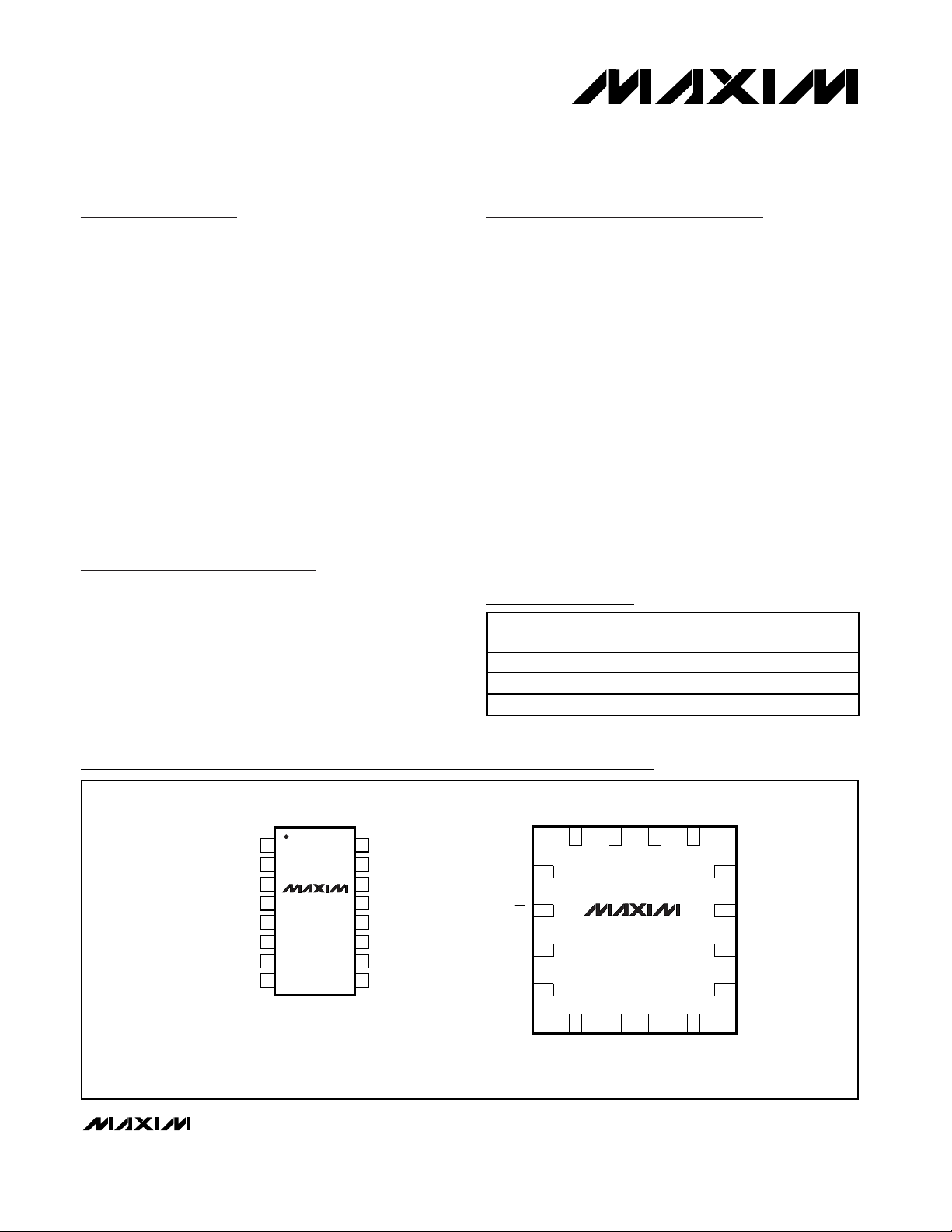
Pin Configurations
Ordering Information
19-2049; Rev 3; 1/05
For pricing, delivery, and ordering information, please contact Maxim/Dallas Direct! at
1-888-629-4642, or visit Maxim’s website at www.maxim-ic.com.
Ordering Information continued at end of data sheet.
Functional Diagram appears at end of data sheet.
SPI is a trademark of Motorola, Inc.
PART TEMP RANGE
MAX5408EEE -40°C to +85°C 16 QSOP 1
MAX5408ETE -40°C to +85°C 16 Thin QFN 1
MAX5409EEE -40°C to +85°C 16 QSOP 2
PIN-
PACKAGE
WIPERS PER
RESISTOR
TOP VIEW
1
DOUT V
2
DIN
SCLK
3
MAX5408-
4
CS
H0
W0A
N.C. (W0B)
L0
5
6
7
8
MAX5411
QSOP
(5mm x 6mm)
16
15
14
13
12
11
10
9
DD
V
LOGIC
GND
AGND
H1
L1
W1A
N.C. (W1B)
( ) ARE FOR MAX5409/MAX5411 ONLY
SCLK
CS
H0
L0
DIN
16 15 14 13
1
2
3
4
5
N.C. (W0B)
W0A
DOUT
MAX5408-
MAX5411
6
N.C. (W1B)
THIN QFN
(4mm x 4mm)
V
V
DD
LOGIC
78
W1A
12
GND
11
AGND
10
H1
9
L1
Page 2
VDD, V
LOGIC
, CS, SCLK, DIN to GND......................-0.3V to +6V
H_, L_, and W_ to GND ..............................-0.3V to (V
DD
+ 0.3V)
DOUT to GND.............................................-0.3V to (V
DD
+ 0.3V)
AGND to GND .......................................................-0.3V to +0.3V
Input and Output Latchup Immunity...............................±200mA
Maximum Continuous Current into H_, L_, and W_.........±500µA
Continuous Power Dissipation (T
A
= +70°C)
16-Pin QSOP (derate 8.3mW/°C above +70°C)........666.7mW
16-Pin QFN (derate 18.5mW/°C above +70°C) .........1481mW
Operating Temperature Range ...........................-40°C to +85°C
Storage Temperature Range .............................-60°C to +150°C
Maximum Junction Temperature .....................................+150°C
Lead Temperature (soldering, 10s) .................................+300°C
MAX5408–MAX5411
Dual, Audio, Log Taper Digital Potentiometers
2 _______________________________________________________________________________________
ABSOLUTE MAXIMUM RATINGS
ELECTRICAL CHARACTERISTICS
(VDD= +2.7V to +3.6V (MAX5408/MAX5409), VDD= +4.5V to +5.5V (MAX5410/MAX5411), VH_= VDD, VL_= 0, TA= T
MIN
to T
MAX
.
Typical values are at T
A
= +25°C, unless otherwise specified.)
Stresses beyond those listed under “Absolute Maximum Ratings” may cause permanent damage to the device. These are stress ratings only, and functional
operation of the device at these or any other conditions beyond those indicated in the operational sections of the specifications is not implied. Exposure to
absolute maximum rating conditions for extended periods may affect device reliability.
End-to-End Resistance 71013kΩ
Maximum Bandwidth (Note 1) CW_ = 50pF 100 kHz
Absolute Tolerance ±0.25 dB
Tap-to-Tap Tolerance ±0.1 dB
Total Harmonic Distortion + Noise THD+N VIN = 1V
Channel Isolation -100 dB
Interchannel Matching f = 20Hz to 20kHz, tap = -6dB ±0.5 dB
Mute Attenuation -90 dB
Power-Supply Rejection Ratio PSRR -80 dB
Wiper Resistance R
Wiper Capacitance C
Digital Clock Feedthrough f
End-to-End Resistance
Temperature Coefficient
Ratiometric Resistance
Temperature Coefficient
DIGITAL INPUTS (V
Input High Voltage V
Input Low Voltage V
Input Leakage Current ±1 µA
Input Capacitance 5pF
DIGITAL INPUTS (V
Input High Voltage V
Input Low Voltage V
Input Leakage Current ±1 µA
Input Capacitance 5pF
PARAMETER SYMBOL CONDITIONS MIN TYP MAX UNITS
W
W
SCLK
> 4.5V)
LOGIC
IH
IL
< 4.5V)
LOGIC
IH
IL
, f = 1kHz, tap = -6dB 0.002 %
RMS
= 20Hz to 20kHz, tap = -6dB -90 dB
V
1000 1700 Ω
10 pF
35 ppm/°C
5 ppm/°C
2.4 V
0.8 V
0.7 x
LOGIC
0. 3 x
V
LOGIC
V
V
Page 3
MAX5408–MAX5411
Dual, Audio, Log Taper Digital Potentiometers
_______________________________________________________________________________________ 3
ELECTRICAL CHARACTERISTICS (continued)
(VDD= +2.7V to +3.6V (MAX5408/MAX5409), VDD= +4.5V to +5.5V (MAX5410/MAX5411), VH_= VDD, VL_= 0, TA= T
MIN
to T
MAX
.
Typical values are at T
A
= +25°C, unless otherwise specified.)
Note 1: Guaranteed by design, not production tested.
Note 2: Supply current measured while changing wiper position with zero crossing enabled.
Note 3: Supply current measured while wiper position is fixed.
PARAMETER SYMBOL CONDITIONS MIN TYP MAX UNITS
DIGITAL OUTPUT
Output High Voltage V
Output Low Voltage V
TIMING CHARACTERISTICS (Figure 1)
SCLK Clock Period t
SCLK Pulse Width High t
SCLK Pulse Width Low t
CS Fall to SCLK Rise Setup
Time
SCLK Rise to CS Rise Hold Time t
DIN Setup Time t
DIN Hold Time t
SCLK Fall to DOUT Valid
Propagation Delay
CS Rise to SCLK Rise Hold Time t
CS Pulse Width High t
Wiper Settling Time t
POWER SUPPLIES
Supply Voltage V
Active Supply Current f
Standby Supply Current
Logic Supply Voltage V
Logic Active Supply Current f
Logic Standby Supply Current
OH
OL
CP
CH
CL
t
CSS
CSH
DS
DH
t
DO
CS1
CSW
IW
I
SOURCE
I
= 2mA 0.4 V
SINK
C
LOAD
Zero-crossing detect disabled 1 µs
MAX5408/MAX5409 2.7 3.6
DD
I
DD
LOGIC
I
LOGIC
MAX5410/MAX5411 4.5 5.5
SCLK
(Note 3) 0.2 10
= 2M H z, D OU T = fl oati ng ( N ote 2) 120
S C L K
DOUT = floating (Note 3) 0.5 10
V
= 0.5mA
LOGIC
- 0.5
100 ns
40 ns
40 ns
40 ns
0ns
40 ns
0ns
= 200pF 80 ns
40 ns
100 ns
= 2MHz (Note 2) 100
2.7 5.5 V
µA
µA
V
V
Page 4
MAX5408–MAX5411
Dual, Audio, Log Taper Digital Potentiometers
4 _______________________________________________________________________________________
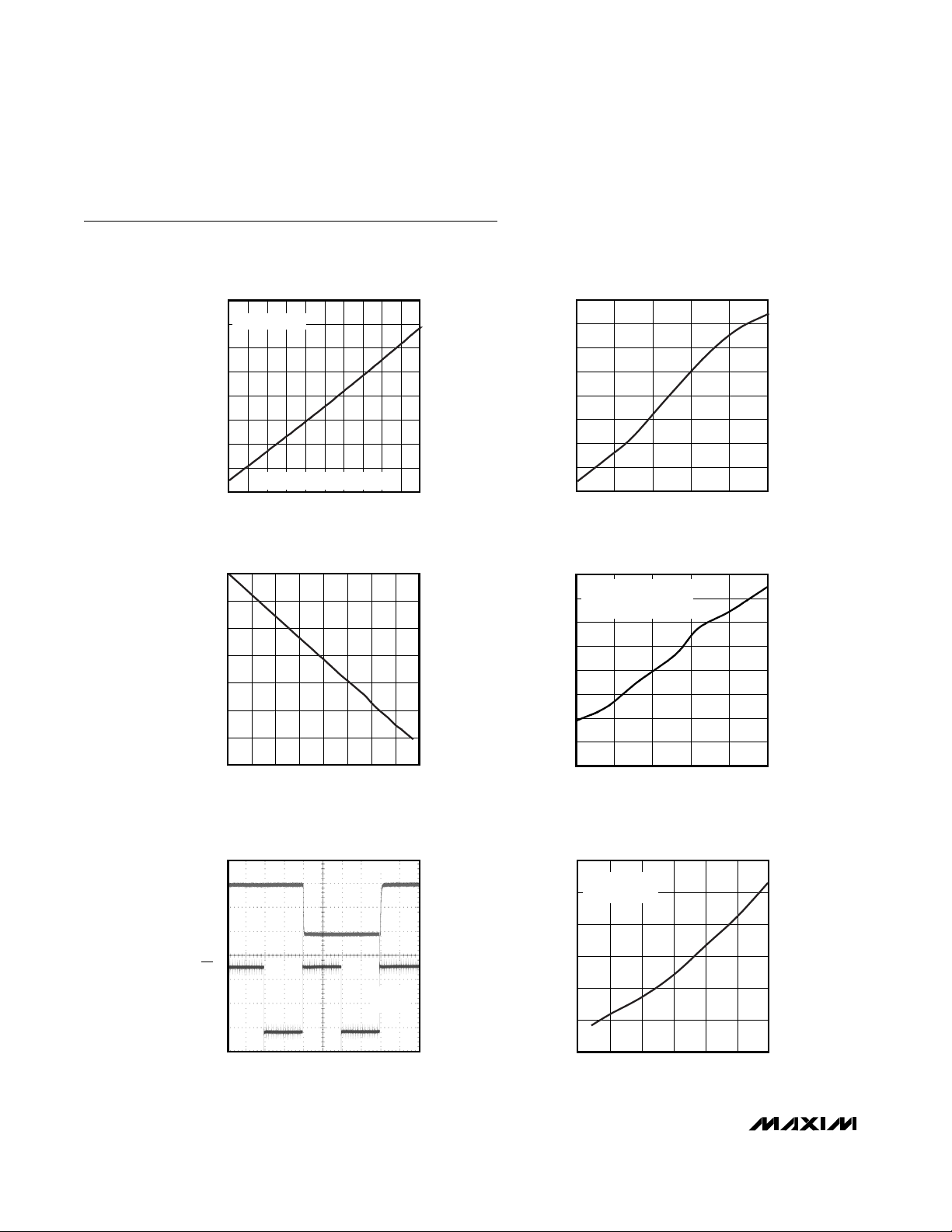
Typical Operating Characteristics
(VDD= +3V (MAX5408/MAX5409), VDD= +5V (MAX5410/MAX5411), DOUT = floating)
988
990
989
991
994
995
993
992
996
0 1.0 1.5 2.0 2.50.5 3.0 3.5 4.0 4.5 5.0
WIPER RESISTANCE vs.
WIPER VOLTAGE
MAX5408-11 toc01
WIPER VOLTAGE (V)
WIPER RESISTANCE (Ω)
TAP POSITION 31
VDD = 5V = V
LOGIC
, L_ = GND
-0.20
-0.15
-0.10
-0.05
0
0.05
0.10
0.15
0.20
-40 -15 10 35 60 85
END-TO-END RESISTANCE % CHANGE
vs. TEMPERATURE
MAX5408-11 toc02
TEMPERATURE (°C)
END-TO-END RESISTANCE CHANGE (%)
-70
-60
-40
-50
-20
-10
-30
0
081241620242832
ATTENUATION vs. TAP POSITION
MAX5408-11 toc03
TAP POSITION
ATTENUATION (dB)
20
25
30
35
40
45
50
55
60
-40 -15 10 35 60 85
TOTAL SUPPLY CURRENT
VS. TEMPERATURE
MAX5408-11 toc04
TEMPERATURE (°C)
TOTAL SUPPLY CURRENT (µA)
ZERO-CROSSING ENABLED
I
TOTAL
= I
DD
+ I
LOGIC
ACTIVE MODE
4µs/div
TAP-TO-TAP SWITCHING TRANSIENT
(ZERO-CROSSING DISABLE)
V
W_
2V/div
CS
2V/div
MAX5408-11 toc05
VH_ = 5V
V
L
_ = 0
0
0.10
0.05
0.20
0.15
0.25
0.30
2.5 3.5 4.03.0 4.5 5.0 5.5
LOGIC CURRENT
vs. LOGIC VOLTAGE
MAX5408-11 toc06
LOGIC SUPPLY VOLTAGE (V)
LOGIC SUPPLY CURRENT (µA)
STANDBY MODE
SCLK = GND
Page 5

MAX5408–MAX5411
Dual, Audio, Log Taper Digital Potentiometers
_______________________________________________________________________________________ 5
Typical Operating Characteristics (continued)
(VDD= +3V (MAX5408/MAX5409), VDD= +5V (MAX5410/MAX5411), DOUT = floating)
0
15
10
5
20
25
30
35
40
45
50
2.5 3.53.0 4.0 4.5 5.0 5.5
LOGIC CURRENT
vs. LOGIC VOLTAGE
MAX5408-11 toc07
LOGIC SUPPLY VOLTAGE (V)
LOGIC SUPPLY CURRENT (µA)
ACTIVE MODE
SCLK = 2MHz, O to V
LOGIC
0
0.05
0.10
0.15
0.20
0.25
0.30
0.35
0.40
0.45
0.50
0.55
2.5 3.0 3.5 4.0 4.5 5.0 5.5
SUPPLY CURRENT
vs. SUPPLY VOLTAGE
MAX5408-11 toc08
VDD (V)
I
DD
(µA)
ZERO-CROSSING DETECTION DISABLED
ACTIVE
STANDBY
Pin Description
(
M A X5 4 0 8 /
M A X5 4 1 0
Q F N )
1313SCLK Serial Clock Input
2424CS Chip-Select Input
3535H0 High Terminal of Resistor 0
4646L0 Low Terminal of Resistor 0
5757W0A Wiper Terminal A of Resistor 0
—— 68W0B Wiper Terminal B of Resistor 0
—— 79W1B Wiper Terminal B of Resistor 1
810810 W1A Wiper Terminal A of Resistor 1
911911 L1 Low Terminal of Resistor 1
10 12 10 12 H1 High Terminal of Resistor 1
11 13 11 13 AGND Analog Ground
12 14 12 14 GND Ground
13 15 13 15 V
14 16 14 16 V
15 1 15 1 DOUT Serial Data Output
16 2 16 2 DIN Serial Data Input
6, 7 8, 9 — — N.C. No Connection. Not internally connected.
PIN
M A X5 4 0 8 /
M A X5 4 1 0 ( Q SO P)
M A X5 4 0 9 /
M A X5 4 1 1 ( Q F N )
M A X5 4 0 9 /
M A X5 4 1 1 ( Q SO P)
NAME FUNCTION
LOGIC
Digital Logic Power Supply
Analog Power Supply
DD
Page 6

MAX5408–MAX5411
Dual, Audio, Log Taper Digital Potentiometers
6 _______________________________________________________________________________________
Detailed Description
Digital Serial Interface
An SPI-compatible serial interface controls the
MAX5408–MAX5411. The input word to the device is
eight bits long, composed of three address bits (A0,
A1, and A2), followed by five data bits, with MSB first
(see Tables 1 and 2). The first three address bits set
the value of internal registers. The five data bits control
the wiper position. For certain commands, some of the
five data bits are “don’t cares”, but must be sent to the
device.
The serial data is listed in Tables 1 and 2.
The control code determines:
• Potentiometer to update or register to set.
• Data for mute register (Tables 3 and 4).
• Data for zero-crossing detection register (Tables 5
and 6).
The data bits control the position of the wiper (Table 7).
A logic low on the chip-select input (CS) enables the
device’s serial interface. A logic high on CS disables
the interface control circuitry. See Figure 1 for serialinterface timing description.
Table 1. Serial Interface Programming Commands for MAX5408/MAX5410
Figure 1. Serial Timing Diagram
8-BIT SERIAL WORD
A0 A1 A2 D4–D0
00 05-bit DAC data Set position of wiper W0A
00 15-bit DAC data No change
01 05-bit DAC data Set position of wiper W1A
01 15-bit DAC data No change
10 04-bit mute data, D0 = “don’t care” Data for mute register (see Table 3)
10 1
4-bit zero-crossing detection data,
D0 = “don’t care”
11 000000
Data for zero-crossing detection register
(see Table 5)
Readback contents of wiper register for W0A
at DOUT
11 000001 No change
11 000010
Readback contents of wiper register for W1A
at DOUT
11 000011 No change
11 000100 Readback contents of mute register at DOUT
11 000101
Readback contents of zero-crossing detection
register at DOUT
Immediate update then analog power-down
11 1D4 = 0, D3–D0 = “don’t care”
when zero crossing is enabled. No effect
when zero crossing is disabled.
CS
t
SCLK
DIN
DOUT
CS
SCLK
DIN
DOUT
WIPER
CSS
t
DS
t
DH
FUNCTION
t
CL
t
CP
t
DO
t
CH
t
CSW
t
CSH
t
CSI
t
IW
Page 7

MAX5408–MAX5411
Dual, Audio, Log Taper Digital Potentiometers
_______________________________________________________________________________________ 7
Table 2. Serial Interface Programming Commands for MAX5409/MAX5411
Table 3. Mute Register Bit Definitions for MAX5408/MAX5410
Table 4. Mute Register Bit Definitions for MAX5409/MAX5411
A0 A1 A2 D4–D0
0005-bit DAC data Set position of wiper W0A
0015-bit DAC data Set position of wiper W0B
0105-bit DAC data Set position of wiper W1A
0115-bit DAC data Set position of wiper W1B
100
101
11000000 Readback contents of wiper register for W0A at DOUT
11000001 Readback contents of wiper register for W0B at DOUT
11000010 Readback contents of wiper register for W1A at DOUT
11000011 Readback contents of wiper register for W1B at DOUT
11000100 Readback contents of mute register at DOUT
11000101 Readback contents of zero-crossing detection register at DOUT
111D4 = 0, D3–D0 = “don’t care” Analog power-down
111D4 = 1, D3–D0 = “don’t care” Analog power-up
8-BIT SERIAL WORD
4-bit mute data, D0 = “don’t care”
4-bit zero-crossing detection data,
D0 = “don’t care”
FUNCTION
Data for mute register (see Table 4)
Data for zero-crossing detection register
(see Table 6)
DATA BIT VALUE FUNCTION
D4
D3 “don’t care” No change
D2
D1 “don’t care” No change
D0 “don’t care” No change
DATA BIT VALUE FUNCTION
D4
D3
D2
D1
D0 “don’t care” No change
0 Set wiper W0A to preprogrammed value (-62dB on power-up)
1 Set wiper W0A to mute (-90dB)
0 Set wiper W1A to preprogrammed value (-62dB on power-up)
1 Set wiper W1A to mute (-90dB)
0 Set wiper W0A to preprogrammed value (-62dB on power-up)
1 Set wiper W0A to mute (-90dB)
0 Set wiper W0B to preprogrammed value (-62dB on power-up)
1 Set wiper W0B to mute (-90dB)
0 Set wiper W1A to preprogrammed value (-62dB on power-up)
1 Set wiper W1A to mute (-90dB)
0 Set wiper W1B to preprogrammed value (-62dB on power-up)
1 Set wiper W1B to mute (-90dB)
Page 8

MAX5408–MAX5411
The digital output, DOUT, lags the digital input signal,
DIN by 8.5 clock cycles. Force CS high to disable
DOUT, placing DOUT in three-state mode. Force CS
low to enable DOUT and disable three-state mode.
Force CS high, after a word has been written to the
MAX5408–MAX5411 to make a readback request. The
next CS low period writes the requested data to DOUT.
A readback request overwrites any previous data in the
shift register. Note that the data appears at DOUT in
the order: A0, A1, A2, D4, D3, D2, D1, D0. A0 will be
available after the first high-to-low transition of SCLK
when CS is low. The input continues to load the shift
register while data is being read out of the MAX5408–
MAX5411. The input data appears at DOUT 8.5 clock
cycles later. A CS transition from low-to-high latches
the input data. For any control byte, the state of SCLK
must be the same for both CS low-to-high transitions
and CS high-to-low transitions in order to preserve the
data at DOUT while CS transitions. For proper operation, ensure that the input data remains valid on both
the SCLK rising and falling edges when daisy chaining
multiple devices.
Zero-Crossing Detection
The zero-crossing detection register enables the zerocrossing detect feature. The zero-crossing detect feature reduces the audible noise (“clicks and pops”) that
result from wiper transitions. The wiper changes position only when the voltage at L_ is the same as the voltage at H_. Each wiper has a zero-crossing and timeout
Dual, Audio, Log Taper Digital Potentiometers
8 _______________________________________________________________________________________
Table 5. Zero-Crossing Detection Register Bit Definitions for MAX5408/MAX5410
Table 6. Zero-Crossing Detection Register Bit Definitions for MAX5409/MAX5411
Table 7. Attenuation and Wiper Position
DATA BIT VALUE FUNCTION
D4
D3 “don’t care” No change
D2
D1 “don’t care” No change
D0 “don’t care” No change
DATA BIT VALUE FUNCTION
D4
D3
D2
D1
D0 “don’t care” No change
0 Disable wiper W0A zero-crossing detection circuit
1 Enable wiper W0A zero-crossing detection circuit
0 Disable wiper W1A zero-crossing detection circuit
1 Enable wiper W1A zero-crossing detection circuit
0 Disable wiper W0A zero-crossing detection circuit
1 Enable wiper W0A zero-crossing detection circuit
0 Disable wiper W0B zero-crossing detection circuit
1 Enable wiper W0B zero-crossing detection circuit
0 Disable wiper W1A zero-crossing detection circuit
1 Enable wiper W1A zero-crossing detection circuit
0 Disable wiper W1B zero-crossing detection circuit
1 Enable wiper W1B zero-crossing detection circuit
POSITION OUTPUT LEVEL (dB)
00
1-2
2-4
3-6
4-8
.
.
.
.
.
30 -60
31 -62
MUTE <-90
.
.
.
.
.
Page 9

MAX5408–MAX5411
Dual, Audio, Log Taper Digital Potentiometers
_______________________________________________________________________________________ 9
Figure 4. Stereo Volume Control with Front and Rear Fade
Figure 3. Attenuation Control
Figure 2. Zero-Crossing Timing Diagram
V
H_
V
H_
V
L_
-10dB
WIPER
POSITION
-20dB
50ms (TYP)t = 0
V
L_
WIPER
POSITION
100ms
CHANGING WIPER POSITIONS WITH ZERO-CROSSING ENABLED, COMMAND ISSUED AT t = 0
MAX5408–
MAX5411
V
IN1
H1
V
OUT1
L1
V
IN0
H0
V
OUT0
W0A W1A
L0
-20dB
50ms (TYP)t = 0
-10dB
100ms
V
LEFT
F
V
R
LEFT
W0A W1A
W0B W1B
V
LEFT
H0
L0
MAX5409/
MAX5411
V
RIGHT
H1
L1
V
F
RIGHT
V
R
RIGHT
Page 10

Chip Information
TRANSISTOR COUNT: 12,875
PROCESS: BiCMOS
MAX5408–MAX5411
Dual, Audio, Log Taper Digital Potentiometers
10 ______________________________________________________________________________________
Figure 6. Gain Control
Figure 5. Daisy-Chaining of Serial Interfaces
Ordering Information (continued)
circuit (see Figure 2). With zero-crossing enabled, the
MAX5408–MAX5411 change wiper position after 50ms
or when zero crossing is detected.
Power-On Reset
The power-on reset (POR) feature sets all the wipers to
the maximum attenuation (tap position 31, -62dB) at
power-up. If either VDDor V
LOGIC
is zero volts, a poweron reset intiates when one of the supplies is brought
back to the operating voltage.
Mute Function
When mute is enabled, the wipers go to -90dB attenuation. When mute is disabled, the wiper returns to its
position before mute was enabled. All wipers can be
muted simultaneously or independently.
Applications Information
Attenuation Control
Figure 3 shows the application of an attenuation control.
The op amps are connected in a follower configuration
with a fixed gain. The digitally controlled potentiometer
attenuates the input signal.
Stereo Volume Control
Figure 4 shows the application of stereo volume control using MAX5409/MAX5411. The op amps are connected in a follower configuration with fixed gain. The
digitally controlled potentiometer attenuates the input
signals. The second wiper of each potentiometer controls the signal amplitude at the rear set of speakers.
Daisy-Chaining
Figure 5 shows an application daisy-chaining the
serial-interfaces of the MAX5408–MAX5411. A singlewrite command updates multiple devices from a single
digital port in this configuration (see Digital Serial
Interface section).
Gain Control
Figure 6 shows the application of a gain control.
Note: Muting the potentiometer creates unpredictable
behavior at the output of the op amp, and may seriously
degrade the performance of the op amp.
SCLK
H1
V
IN1
SDIN
SCLK
SDIN
SCLK
DOUT SDIN
SCLK
DOUT SDIN
DOUT
V
OUT0
H0
V
IN0
W0A W1A
MAX5408–
MAX5411
V
OUT1
MAX5408–
CS
MAX5411
CS
CS
MAX5408–
MAX5411
CS
MAX5408–
MAX541
L0
L1
PART TEMP RANGE
MAX5409ETE -40°C to +85°C 16 Thin QFN 2
MAX5410EEE -40°C to +85°C 16 QSOP 1
MAX5410ETE -40°C to +85°C 16 Thin QFN 1
MAX5411EEE -40°C to +85°C 16 QSOP 2
MAX5411ETE -40°C to +85°C 16 Thin QFN 2
PINPACKAGE
WIPERS PER
RESISTOR
Page 11

MAX5408–MAX5411
Dual, Audio, Log Taper Digital Potentiometers
______________________________________________________________________________________ 11
Functional Diagram
W0A
H0
N.C. (W0B) DOUT W1A H1
MAX5408–
MAX5411
32 POSITION
DECODER/
REGISTER
N.C. (W1B)
AUDIO ZERO-
CROSSING
DETECTOR
SPI LOGIC
V
LOGICVDD GND AGND
( ) ARE FOR MAX5409/MAX5411 ONLY
L0
SCLK DIN CS L1
Page 12
MAX5408–MAX5411
Dual, Audio, Log Taper Digital Potentiometers
12 _______________________________________________________________________________________
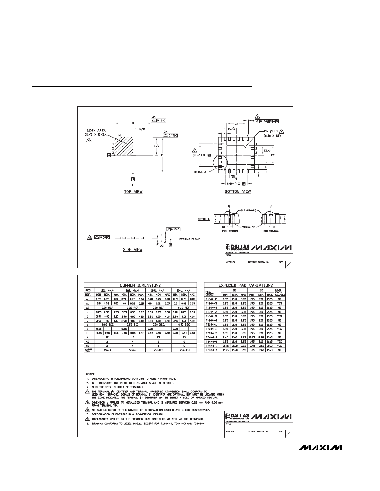
Package Information
(The package drawing(s) in this data sheet may not reflect the most current specifications. For the latest package outline information,
go to www.maxim-ic.com/packages.)
24L QFN THIN.EPS
PACKAGE OUTLINE
12, 16, 20, 24L THIN QFN, 4x4x0.8mm
21-0139
PACKAGE OUTLINE
12, 16, 20, 24L THIN QFN, 4x4x0.8mm
21-0139
1
C
2
2
C
2
Page 13

MAX5408-MAX5411
Dual, Audio, Log Taper Digital Potentiometers
Maxim cannot assume responsibility for use of any circuitry other than circuitry entirely embodied in a Maxim product. No circuit patent licenses are
implied. Maxim reserves the right to change the circuitry and specifications without notice at any time.
Maxim Integrated Products, 120 San Gabriel Drive, Sunnyvale, CA 94086 408-737-7600 ____________________ 13
© 2005 Maxim Integrated Products Printed USA is a registered trademark of Maxim Integrated Products, Inc.
Package Information (continued)
(The package drawing(s) in this data sheet may not reflect the most current specifications. For the latest package outline information,
go to www.maxim-ic.com/packages.)
QSOP.EPS
PACKAGE OUTLINE, QSOP .150", .025" LEAD PITCH
21-0055
1
E
1
 Loading...