

Page 1
General Description
The MAX5407 SOT-PoT™ is a logarithmic taper digital
potentiometer with 32 tap points that has 1dB steps
between taps. This device is ideal for audio applications, such as volume control and fading/balancing
audio signals.
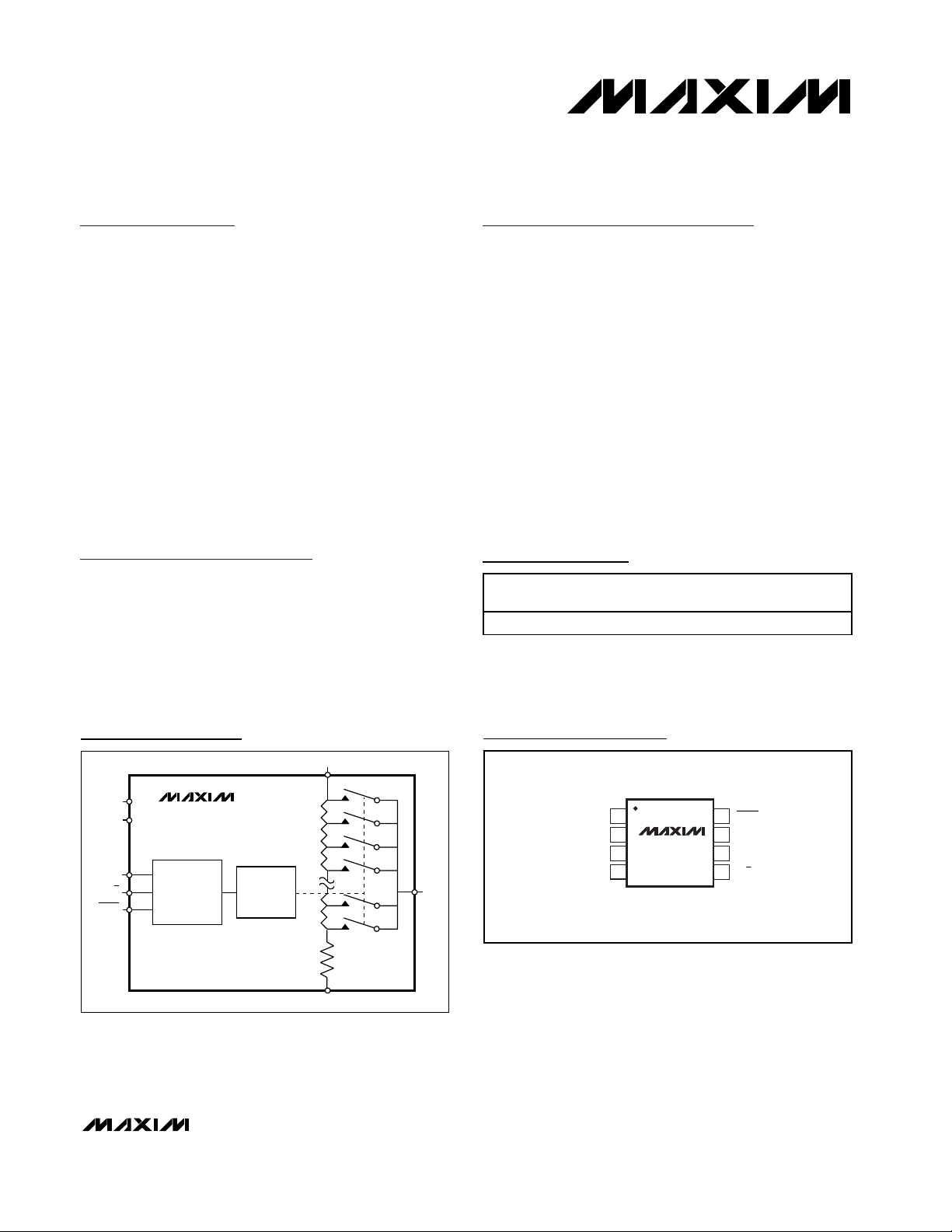
The MAX5407 consists of a resistor string and CMOS
switches that are digitally controlled through a simple 2wire serial interface. This device performs the same
function as a mechanical potentiometer. The device
has a fixed end-to-end resistance of 20kΩ and features
zero-crossing detection to minimize the audible noise
generated by the wiper transitions.
This device has nominal resistor temperature coefficients
of 35ppm/°C end-to-end and 5ppm/°C ratiometric. The
MAX5407 is available in a space saving 8-pin SOT23
package and is guaranteed from -40°C to +85°C.
Applications
Audio Volume Control
Fading/Balancing Audio Signals
Mechanical Potentiometer Replacement
Features
♦ Miniature 3mm x 3mm 8-Pin SOT23 Package
♦ Logarithmic Taper with 1dB Steps Between Taps
♦ 32 Tap Positions
♦ Low 0.35µA Supply Current
♦ +2.7V to +5.5V Single-Supply Operation
♦ Zero-Crossing Detection to Minimize Audible
Clicks During Wiper Transitions
♦ Simple Up/Down 2-Wire Serial Data Interface
♦ Power-On Reset
Wiper Goes To Maximum Attenuation
(Lowest Tap Position)
♦ 20kΩ End-to-End Resistance
MAX5407
32-Tap Audio Logarithmic Taper
Digital Potentiometer
________________________________________________________________ Maxim Integrated Products 1
Pin Configuration
Ordering Information
UP/DOWN
COUNTER
V
DD
GND
CS
H
L
W
U/D
ZCEN
32-POSITION
DECODER
MAX5407
Functional Diagram
19-2196; Rev 0; 10/01
For pricing, delivery, and ordering information, please contact Maxim/Dallas Direct! at
1-888-629-4642, or visit Maxim’s website at www.maxim-ic.com.
SOT-PoT is a trademark of Maxim Integrated Products, Inc.
PART TEMP. RANGE
MAX5407EKA -40°C to +85°C 8 SOT23 AAID
PIN-
PACKAGE
TOP MARK
TOP VIEW
1
H
2
GND
3
W
4
ZCEN
8
V
7
MAX5407
SOT23
DD
6
CS
5
U/DL
Page 2
MAX5407
32-Tap Audio Logarithmic Taper
Digital Potentiometer
2 _______________________________________________________________________________________
ABSOLUTE MAXIMUM RATINGS
ELECTRICAL CHARACTERISTICS
(VDD= +2.7V to +5.5V, VH= VDD, VL= 0, TA= T
MIN
to T
MAX
, unless otherwise noted. Typical values are at VDD= +5V and TA= +25°C.)
(Note 1)
Stresses beyond those listed under “Absolute Maximum Ratings” may cause permanent damage to the device. These are stress ratings only, and functional
operation of the device at these or any other conditions beyond those indicated in the operational sections of the specifications is not implied. Exposure to
absolute maximum rating conditions for extended periods may affect device reliability.
VDDto GND..............................................................-0.3V to +6V
H, W, L, CS, ZCEN, and U/D to GND .........-0.3V to (V
DD
+ 0.3V)
Input and Output Latchup Immunity...............................±200mA
Maximum Continuous Current into H, L, and W ..............±500µA
Continuous Power Dissipation (T
A
= +70°C)
8-Pin SOT23-8 (derate 8.9mW/°C above +70°C) ......714mW
Operating Temperature Range ...........................-40°C to +85°C
Junction Temperature......................................................+150°C
Storage Temperature Range .............................-65°C to +150°C
Soldering Temperature (soldering, 10s) ..........................+300°C
Number of Resistor Taps 32 Taps
End-to-End Resistance 15 20 25 kΩ
Bandwidth (Note 2) (Notes 3, 4) 500 kHz
Absolute Tolerance (Note 5) (Note 3) ±0.25 ±1 dB
Tap-to-Tap Tolerance (Note 6) (Note 3) ±0.05 ±0.1 dB
Total H ar m oni c D i stor ti on + N oi se THD + N
Power-Supply Rejection Ratio PSRR -80 dB
End-to-End Resistance
Temperature Coefficient
Ratiometric Resistance
Temperature Coefficient
Wiper Resistance R
DIGITAL INPUTS
Input High Voltage V
Input Low Voltage V
Input Leakage Current ±1 µA
Input Capacitance 5pF
TIMING CHARACTERISTICS (Figures 1, 2)
U/D Mode to CS Setup t
CS to U/D Step Setup t
CS to U/D Step Hold
U/D Step Low Period
U/D Step High Period t
Up/Down Toggle Rate f
PARAMETER SYMBOL CONDITIONS MIN TYP MAX UNITS
TC
R
W
IH
IL
CU
CI
t
IC
t
IL
IH
TOGGLE
V
= 1V
IN
Tap = -6dB (Notes 3, 4)
VDD = 2.7V 400 1700 Ω
RMS
, f = 1kHz,
2.4 V
0.002 %
35 ppm/°C
5 ppm/°C
0.8 V
25 ns
25 ns
25 ns
25 ns
25 ns
7 MHz
Wiper Switching Time t
Zero-Crossing Timeout 50 ms
IW
Zero-crossing detection disabled (Note 4) 0.1 µs
Page 3
MAX5407
32-Tap Audio Logarithmic Taper
Digital Potentiometer
_______________________________________________________________________________________ 3
ELECTRICAL CHARACTERISTICS (continued)
(VDD= +2.7V to +5.5V, VH= VDD, VL= 0, TA= T
MIN
to T
MAX
, unless otherwise noted. Typical values are at VDD= +5V and TA= +25°C.)
(Note 1)
Note 1: All devices are 100% production tested at TA= +25°C and guaranteed by design for TA= T
MIN
to T
MAX
.
Note 2: Bandwidth is measured from H to W at the -6dB wiper tap position (see Typical Operating Characteristics).
Note 3: These specifications are only valid for I
W
less than 100nA of continuous wiper current.
Note 4: Measured with 20pF load capacitor.
Note 5: Absolute tolerance is defined as the variation of the attenuation for any given tap from its expected value.
Note 6: Tap-to-tap tolerance is defined as the variation between any two adjacent taps from the typical value of 1dB.
Note 7: Supply current when f
TOGGLE
= 2MHz.
Note 8: Supply current when wiper position is not changing.
Typical Operating Characteristics
(VDD= +5V, TA = +25°C, unless otherwise noted.)
100
150
250
200
300
350
021345
WIPER RESISTANCE vs.
WIPER VOLTAGE
MAX5407 toc01
WIPER VOLTAGE (V)
WIPER RESISTANCE (Ω)
VDD = +3V
VDD = +5V
-0.25
-0.20
-0.15
-0.10
-0.05
0
0.05
0.10
0.15
-40 -15 10 35 60 85
END-TO-END RESISTANCE %
CHANGE vs. TEMPERATURE
MAX5407 toc02
TEMPERATURE (°C)
ENE-TO-END RESISTANCE CHANGE (%)
-35
-30
-20
-25
-10
-5
-15
0
08124 1620242832
ATTENUATION vs. TAP POSITION
MAX5407 toc03
TAP POSITION
ATTENUATION (dB)
PARAMETER SYMBOL CONDITIONS MIN TYP MAX UNITS
POWER SUPPLIES
Supply Voltage V
Supply Current I
DD
DD
All digital
inputs are
set to 0
Active (Note 7) 100
S tand b y ( N ote 8) 0.35 1
2.7 5.5 V
µA
Page 4

MAX5407
32-Tap Audio Logarithmic Taper
Digital Potentiometer
4 _______________________________________________________________________________________
32-Tap Audio Logarithmic Taper
Digital Potentiometer
Typical Operating Characteristics (continued)
(VDD= +5V, TA = +25°C, unless otherwise noted.)
0
-5
-10
-15
-20
0.001 10.01 0.1 10 100 1000
FREQUENCY RESPONSE
MAX5407 toc07
FREQUENCY (kHz)
GAIN (dB)
TAP POSITION 6
0.00001
0.0001
0.001
0.01
TOTAL HARMONIC DISTORTION + NOISE
vs. FREQUENCY
MAX5407 toc08
FREQUENCY (kHz)
THD+N (%)
0.01 10.1 10 100
TAP POSITION 6
Pin Description
SUPPLY CURRENT vs. TEMPERATURE
0.50
0.45
0.40
0.35
0.30
0.25
0.20
0.15
SUPPLY CURRENT (µA)
0.10
0.05
0
-40 10-15 35 60 85
VDD = +3V
TEMPERATURE (°C)
MAX5407 toc04
VDD = +5V
OUTPUT
200mV/div
TAP-TO-TAP SWITCHING TRANSIENT
U/D
2V/div
W
40ns/div
MAX5407 toc05
STANDBY SUPPLY CURRENT vs.
SUPPLY VOLTAGE
0.40
0.35
0.30
0.25
0.20
0.15
0.10
STANDBY SUPPLY CURRENT (µA)
0.05
0
2.5 3.53.0 4.0 4.5 5.0 5.5
SUPPLY VOLTAGE (V)
MAX5407 toc06
PIN NAME FUNCTION
1 H High Terminal of Resistor
2 GND Ground
3 W Wiper Terminal of Resistor
4 L Low Terminal of Resistor
5U/D
6CS
7VDDPower Supply
8 ZCEN Zero-Crossing Detection Enable Input. Set to low to enable zero-crossing detection.
Up/Down Control Input. With CS high, a low-to-high transition increments or decrements the wiper
position, depending on the mode.
Chip-Select Input. A low-to-high CS transition determines the mode: increment
if U/D is high, decrement if U/D is low.
Page 5

Detailed Description
Digital Interface Operation
The MAX5407 has two modes of operation when the serial interface is active: increment and decrement mode.
The serial interface is only active when CS is high.
The CS and U/D inputs control the position of the wiper
along the resistor array. When CS transitions from low
to high, the part will go into increment mode if U/D is
high and into decrement mode if U/D is low. Once the
mode is set, the device will remain in that mode until CS
goes low again. A low-to-high transition at the U/D pin
will increment or decrement the wiper position depending on the mode (Figures 1 and 2).
When the CS input transitions to low (serial interface
inactive), the value of the counter is stored and the
wiper position is maintained.
MAX5407
32-Tap Audio Logarithmic Taper
Digital Potentiometer
_______________________________________________________________________________________ 5
U/D
Figure 1. Serial Interface Timing Diagram, Increment Mode
Figure 2. Serial Interface Timing Diagram, Decrement Mode
CS
t
CU
t
IL
t
IC
W
NOTE: W IS NOT A DIGITAL SIGNAL. IT REPRESENTS THE WIPER TRANSITIONING.
CS
t
CU
U/D
W
t
CI
t
IW
t
IH
t
CI
t
IH
t
IC
t
IL
NOTE: W IS NOT A DIGITAL SIGNAL. IT REPRESENTS THE WIPER TRANSITIONING.
t
IW
Page 6
MAX5407
Power-On Reset
The power-on reset feature sets the wiper to the maximum attenuation (tap position 31, -31dB) at power-up.
If CS is initially high, the MAX5407 is in the increment
mode by default.
Zero-Crossing Detection
When the ZCEN input is low, the zero-crossing detect
feature is enabled. This feature reduces the audible
noise (“clicks and pops”) that result from wiper transitions. When zero-crossing detection is enabled, the
wiper changes position only when the voltage at L is
the same as the voltage at H. If no zero crossing is
detected after 50ms, the device will timeout and
change the wiper position.
Digital Logic Inputs
The MAX5407 can interface to +3V logic as well as +5V
logic, while using a +3V to +5V power supply. In order
to minimize the supply current, set all digital inputs low
while the part is inactive.
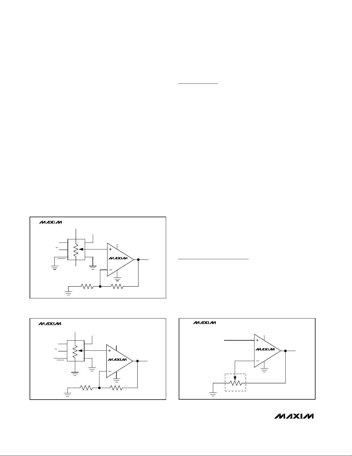
Applications Information
The MAX5407 is intended for circuits requiring digitally
controlled adjustable voltage or adjustable gain, such
as applications involving volume control.
Volume Control
The zero-crossing feature of the MAX5407 makes it
ideal for applications involving volume control. Figure 3
shows a typical application circuit, where the MAX5407
is followed by an op amp for output buffering and gain.
VCMrepresents the common voltage around which the
audio signal swings.
Signal Attenuator
Figure 4 shows a typical signal attenuator. Use an op
amp to provide buffering and gain to the output of the
MAX5407. Connect the MAX5407 to the positive input
of a noninverting op amp to select the level of attenuation of the input signal, by digitally controlling the wiper
terminal.
Adjustable Gain
Figure 5 shows how to use the MAX5407 to digitally
adjust the gain of a noninverting op amp configuration.
The MAX5407 has a low 5ppm/°C ratiometric tempco
that allows for a very stable adjustable gain configuration over temperature.
Chip Information
TRANSISTOR COUNT: 1942
32-Tap Audio Logarithmic Taper
Digital Potentiometer
6 _______________________________________________________________________________________
Figure 3. Volume Control Circuit
Figure 4. Signal Attenuator Circuit
Figure 5. Adjustable Gain Circuit
U/D
CS
ZCEN
AUDIO INPUT
H
L
V
CM
+5V
V
V
DD
W
DD
MAX4336
MAX5407
V
OUT
MAX5407
+5V
CS
U/D
SIGNAL INPUT
ZCEN
H
L
+5V
V
V
DD
W
DD
MAX4336
V
OUT
MAX5407
V
DD
V
IN
MAX4336
W
LH
MAX5407
V
OUT
Page 7
MAX5407
32-Tap Audio Logarithmic Taper
Digital Potentiometer
Maxim cannot assume responsibility for use of any circuitry other than circuitry entirely embodied in a Maxim product. No circuit patent licenses are
implied. Maxim reserves the right to change the circuitry and specifications without notice at any time.
Maxim Integrated Products, 120 San Gabriel Drive, Sunnyvale, CA 94086 408-737-7600 _____________________ 7
© 2001 Maxim Integrated Products Printed USA is a registered trademark of Maxim Integrated Products.
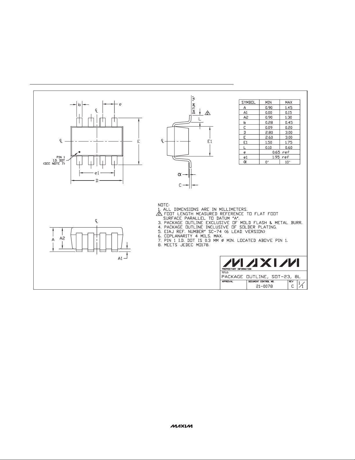
Package Information
SOT23, 8L.EPS
 Loading...