

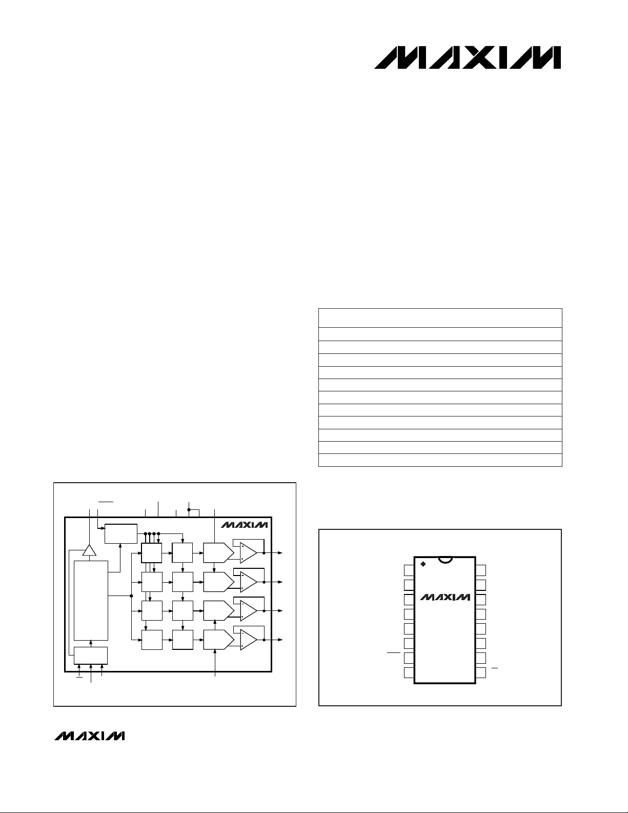
_______________General Description
The MAX536/MAX537 combine four 12-bit, voltage-output
digital-to-analog converters (DACs) and four precision
output amplifiers in a space-saving 16-pin package.
Offset, gain, and linearity are factory calibrated to provide
the MAX536’s ±1LSB total unadjusted error. The MAX537
operates with ±5V supplies, while the MAX536 uses -5V
and +12V to +15V supplies.
Each DAC has a double-buffered input, organized as
an input register followed by a DAC register. A 16-bit
serial word is used to load data into each input/DAC
register. The serial interface is compatible with either
SPI/QSPI™ or Microwire™, and allows the input and
DAC registers to be updated independently or simultaneously with a single software command. The DAC registers can be simultaneously updated with a hardware
LDAC pin. All logic inputs are TTL/CMOS compatible.
________________________Applications
Industrial Process Controls
Automatic Test Equipment
Digital Offset and Gain Adjustment
Motion Control Devices
Remote Industrial Controls
Microprocessor-Controlled Systems
____________________________Features
♦ Four 12-Bit DACs with Output Buffers
♦ Simultaneous or Independent Control of Four
DACs via a 3-Wire Serial Interface
♦ Power-On Reset
♦ SPI/QSPI and Microwire Compatible
♦ ±1LSB Total Unadjusted Error (MAX536)
♦ Full 12-Bit Performance without Adjustments
♦ ±5V Supply Operation (MAX537)
♦ Double-Buffered Digital Inputs
♦ Buffered Voltage Output
♦ 16-Pin DIP/SO Packages
______________Ordering Information
Ordering Information continued at end of data sheet.
* Contact factory for dice specifications.
** Contact factory for availability and processing to MIL-STD-883.
MAX536/MAX537
Calibrated, Quad, 12-Bit
Voltage-Output DACs with Serial Interface
________________________________________________________________
Maxim Integrated Products
1
16
15
14
13
12
11
10
9
1
2
3
4
5
6
7
8
OUTC
OUTD
V
DD
TP
AGND
V
SS
OUTA
OUTB
TOP VIEW
MAX536
MAX537
REFCD
SDO
SCK
CS
SDI
LDAC
DGND
REFAB
DIP/SO
__________________Pin Configuration
MAX536/MAX537
DAC A
DAC
REG A
INPUT
REG A
DAC B
DAC
REG B
INPUT
REG B
DAC C
DAC
REG C
INPUT
REG C
DAC D
DAC
REG D
INPUT
REG D
DECODE
CONTROL
OUTA
OUTB
OUTC
OUTD
16-BIT
SHIFT
REGISTER
SR
CONTROL
CS
SDI
SCK
SDO LDAC
AGND
DGND
VSSTP
V
DD
REFAB
REFCD
________________Functional Diagram
SPI and QSPI are trademarks of Motorola, Inc. Microwire is a trademark of National Semiconductor Corp.
PART TEMP. RANGE PIN-PACKAGE
MAX536ACPE
0°C to +70°C 16 Plastic DIP
MAX536BCPE 0°C to +70°C 16 Plastic DIP
MAX536ACWE 0°C to +70°C 16 Wide SO
MAX536AEPE -40°C to +85°C 16 Plastic DIP
MAX536BCWE 0°C to +70°C 16 Wide SO
±1⁄
2
±1
±1⁄
2
±1
±1⁄
2
INL
(LSB)
19-0230; Rev 2a; 1/97
MAX536BEPE -40°C to +85°C 16 Plastic DIP ±1
MAX536AEWE -40°C to +85°C 16 Wide SO ±1⁄
2
MAX536BEWE -40°C to +85°C 16 Wide SO ±1
MAX536AMDE -55°C to +125°C 16 Ceramic SB** ±1⁄
2
MAX536BMDE -55°C to +125°C 16 Ceramic SB** ±1
MAX536BC/D 0°C to +70°C Dice* ±1
For free samples & the latest literature: http://www.maxim-ic.com, or phone 1-800-998-8800.
For small orders, phone 408-737-7600 ext. 3468.
TA= T
MIN
to T
MAX
MAX536/MAX537
Calibrated, Quad, 12-Bit
Voltage-Output DACs with Serial Interface
2 _______________________________________________________________________________________
VDDto AGND or DGND
MAX536..................................................................-0.3V, +17V
MAX537....................................................................-0.3V, +7V
V
SS
to AGND or DGND ...............................................-7V, +0.3V
SDI, SCK, CS, LDAC, TP, SDO
to AGND or DGND.....................................-0.3V, (VDD+ 0.3V)
REFAB, REFCD to AGND or DGND .............-0.3V, (VDD+ 0.3V)
OUT_ to AGND or DGND.............................................VDD, V
SS
Maximum Current into Any Pin............................................50mA
Continuous Power Dissipation (T
A
= +70°C)
Plastic DIP (derate 10.53mW/°C above +70°C) .................842mW
Wide SO (derate 9.52mW/°C above +70°C).................762mW
Ceramic SB (derate 10.53mW/°C above +70°C)
..................842mW
Operating Temperature Ranges
MAX53_AC_E/BC_E.............................................0°C to +70°C
MAX53_AE_E/BE_E ..........................................-40°C to +85°C
MAX53_AMDE/BMDE.....................................-55°C to +125°C
Storage Temperature Range.............................-65°C to +150°C
Lead Temperature (soldering, 10sec).............................+300°C
ELECTRICAL CHARACTERISTICS—MAX536
(VDD= +15V, VSS= -5V, REFAB/REFCD = 10V, AGND = DGND = 0V, RL= 5kΩ, CL= 100pF, TA= T
MIN
to T
MAX
, unless
otherwise noted. Typical values are at T
A
= +25°C.)
Stresses beyond those listed under “Absolute Maximum Ratings” may cause permanent damage to the device. These are stress ratings only, and functional
operation of the device at these or any other conditions beyond those indicated in the operational sections of the specifications is not implied. Exposure to
absolute maximum rating conditions for extended periods may affect device reliability.
ABSOLUTE MAXIMUM RATINGS
MAX536B
MAX536A
MAX536B
MAX536A
MAX536BM
MAX536AM
MAX536AC
MAX536BC
MAX536AE
MAX536BE
LSB/V±0.03 ±0.30PSRR
LSB/V±0.02 ±0.125PSRR
±2.0
LSB
-0.1 ±1.0
Gain Error
LSB±1DNLDifferential Nonlinearity
±2.0
±1.0
±1
LSB
±0.15 ±0.50
INLIntegral Nonlinearity
±4.0
±3.0
±2.0
±3.0
±2.5
±3.5
UNITSMIN TYP MAXSYMBOLPARAMETER
T
A
= +25°C, -5.5V < VSS< -4.5V
T
A
= +25°C, 10.8V < VDD< 16.5V
RL= 5kΩ
Guaranteed monotonic
CONDITIONS
TUE
Total Unadjusted Error
(Note 1)
LSB
Bits12NResolution
VDDPower-Supply
Rejection Ratio
VSSPower-Supply
Rejection Ratio
TA= +25°C
MAX536_M
MAX536_C/E -0.6 ±1.5
RL= ∞
MAX536B
MAX536A
TA= +25°C
MAX536BM
MAX536AM
MAX536AC
MAX536BC
MAX536AE
MAX536BE
±5.0
Offset Error mV
±2.5
±10.0
±7.5
±5.0
±7.5
±6.1
±8.5
TA= T
MIN
to T
MAX
STATIC PERFORMANCE—ANALOG SECTION
MAX536B
MAX536/MAX537
Calibrated, Quad, 12-Bit
Voltage-Output DACs with Serial Interface
_______________________________________________________________________________________ 3
ELECTRICAL CHARACTERISTICS—MAX536 (continued)
(VDD= +15V, VSS= -5V, REFAB/REFCD = 10V, AGND = DGND = 0V, RL= 5kΩ, CL= 100pF, TA= T
MIN
to T
MAX
, unless
otherwise noted. Typical values are at T
A
= +25°C.)
PARAMETER
SYMBOL CONDITIONS MIN TYP MAX UNITS
Total Unadjusted Error
MAX536A ±1.0
LSB
MAX536B ±2.0
Gain Error ±0.1 ±1.0 LSB
Offset Error
MAX536A ±1.2 ±2.5
mV
±1.2 ±5.0
Integral Nonlinearity INL ±0.2 ±1.0 LSB
Reference Input Range REF 0.0 V
DD
– 4 V
Reference Input Resistance RREF Code dependent, minimum at code 555 hex 5
kΩ
Reference Feedthrough Input code = all 0s
-100
dB
-82
Input High Voltage V
IH
2.4 V
Input Low Voltage V
IL
0.8 V
Input Leakage Current VIN= 0V or V
DD
1.0
µA
Input Capacitance (Note 2) 10 pF
Output Low Voltage V
OL
SDO sinking 5mA 0.18 0.40 V
Output Leakage Current SDO = 0V to V
DD
±10
µA
Voltage-Output Slew Rate 5
V/µs
TUE
MATCHING PERFORMANCE (TA= +25°C)
REFERENCE INPUT
V
REF
= 10Vp-p
at 400Hz
V
REF
= 10Vp-p
at 4kHz
Output Settling Time To ±1⁄2LSB of full scale 3
µs
Digital Feedthrough 5 nV-s
Digital Crosstalk (Note 3) V
REF
= 5V 8 nV-s
Positive Supply Range V
DD
10.8 16.5 V
Negative Supply Range V
SS
-4.5 -5.5 V
DIGITAL INPUTS (SDI, SCK, CS, LDAC)
DIGITAL OUTPUT (SDO)
DYNAMIC PERFORMANCE (RL= 5kΩ, CL= 100pF)
POWER SUPPLIES
I
DD
TA= +25°C 8 18
mA
TA= T
MIN
to T
MAX
25
Negative Supply Current
(Note 4)
I
SS
TA= +25°C -6 -16
TA= T
MIN
to T
MAX
-23
mA
Positive Supply Current
(Note 4)
MULTIPLYING-MODE PERFORMANCE
Reference 3dB Bandwidth kHz700V
REF
= 2Vp-p
Total Harmonic Distortion
Plus Noise
THD + N V
REF
= 2.0Vp-p at 50kHz 0.012 %
MAX536/MAX537
Calibrated, Quad, 12-Bit
Voltage-Output DACs with Serial Interface
4 _______________________________________________________________________________________
ELECTRICAL CHARACTERISTICS—MAX536 (continued)
(VDD= +15V, VSS= -5V, REFAB/REFCD = 10V, AGND = DGND = 0V, RL= 5kΩ, CL= 100pF, TA= T
MIN
to T
MAX
, unless
otherwise noted. Typical values are at T
A
= +25°C.)
PARAMETER
SYMBOL CONDITIONS MIN TYP MAX UNITS
t
POR
20
µs
SCK Clock Period t
CP
100 ns
SCK Pulse Width High t
CH
30 ns
SCK Pulse Width Low t
CL
30 ns
t
CSS
20 ns
t
CSH
10 ns
SDI Setup Time t
DS
40 26 ns
SDI Hold Time t
DH
0 ns
t
DO1
1kΩ pull-up on SDO
to V
DD,
C
LOAD
=
50pF
SDO high 78 105
ns
SDO low 50 80
SCK Fall to SDO Valid
Propagation Delay (Note 7)
t
DO2
1kΩ pull-up on SDO
to V
DD,
C
L
OAD
=
50pF
SDO high 81 110
ns
SDO low 53 85
t
DV
27 45 ns
t
TR
40 60 ns
SCK Rise to CS Fall Delay
t
CS0
Continuous SCK, SCK edge ignored 20 ns
t
CS1
SCK edge ignored 20 ns
LDAC Pulse Width Low
t
LDAC
30 ns
CS Pulse Width High
t
CSW
40 ns
Internal Power-On Reset
Pulse Width (Note 2)
CS Fall to SCK Rise
Setup Time
SCK Rise to CS Rise
Hold Time
SCK Rise to SDO Valid
Propagation Delay (Note 6)
CS Fall to SDO Enable
(Note 8)
CS Rise to SDO Disable
(Note 9)
CS Rise to SCK Rise
Hold Time
Note 1: TUE is specified with no resistive load.
Note 2: Guaranteed by design.
Note 3: Crosstalk is defined as the glitch energy at any DAC output in response to a full-scale step change on any other DAC
.
Note 4: Digital inputs at 2.4V; with digital inputs at CMOS levels, I
DD decreases slightly.
Note 5: All input signals are specified with t
R
= tF≤ 5ns. Logic input swing is 0V to 5V.
Note 6: Serial data clocked out of SDO on SCK’s falling edge. (SDO is an open-drain output for the MAX536. The MAX537’s SDO
pin has an internal active pull-up.)
Note 7: Serial data clocked out of SDO on SCK’s rising edge.
Note 8: SDO changes from High-Z state to 90% of final value.
Note 9: SDO rises 10% toward High-Z state.
TIMING CHARACTERISTICS (Note 5)
MAX536/MAX537
Calibrated, Quad, 12-Bit
Voltage-Output DACs with Serial Interface
_______________________________________________________________________________________ 5
ELECTRICAL CHARACTERISTICS—MAX537
(VDD= +5V, VSS= -5V, REFAB/REFCD = 2.5V, AGND = DGND = 0V, RL= 5kΩ, CL= 100pF, TA= T
MIN
to T
MAX
, unless
otherwise noted. Typical values are at T
A
= +25°C.)
PARAMETER
SYMBOL CONDITIONS MIN TYP MAX UNITS
Resolution N 12 Bits
Integral Nonlinearity INL
MAX537A ±0.15 ±0.50
LSB
MAX537B ±1
Differential Nonlinearity DNL Guaranteed monotonic ±1 LSB
MAX537A ±3.0
MAX537B ±6.0
MAX537AC ±6.0
MAX537BC ±9.0
MAX537AE ±7.0
MAX537BE ±11.0
MAX537AM ±9.0
MAX537BM ±15.0
Gain Error
RL= ∞
-0.3 ±1.5
LSB
RL= 5kΩ
-0.8 ±3.0
PSRR
TA= +25°C, 4.5V ≤ VDD≤ 5.5V
±0.01 ±0.5 LSB/V
PSRR
TA= +25°C, -5.5V ≤ VSS≤ -4.5V
±0.02 ±0.7 LSB/V
Gain Error ±0.1 ±1.25 LSB
Integral Nonlinearity INL ±0.35 ±1.0 LSB
Reference Input Range REF 0.0 VDD- 2.2 V
Offset Error
TA= T
MIN
to T
MAX
mV
VDDPower-Supply
Rejection Ratio
VSSPower-Supply
Rejection Ratio
Offset Error
MAX537A ±0.3 ±3.0
mV
MAX537B ±0.3 ±6.0
Reference Input Resistance RREF Code dependent, minimum at code 555 hex 5
kΩ
Reference 3dB Bandwidth V
REF
= 2Vp-p 700 kHz
Reference Feedthrough Input code = all 0s
-100
dB
MATCHING PERFORMANCE (TA= +25°C)
REFERENCE INPUT
V
REF
= 10Vp-p at 4kHz -82
THD + N V
REF
= 850mVp-p at 100kHz 0.024 %
Input High Voltage V
IH
2.4 V
Input Low Voltage V
IL
0.8 V
Input Leakage Current VIN= 0V or V
DD
1.0
µA
Input Capacitance (Note 2) 10 pF
MULTIPLYING-MODE PERFORMANCE
V
REF
= 10V
p-p
at 400Hz
Total Harmonic Distortion
Plus Noise
DIGITAL INPUTS (SDI, SCK, CS, LDAC)
STATIC PERFORMANCE—ANALOG SECTION
TA= +25°C
MAX537_M
MAX536/MAX537
Calibrated, Quad, 12-Bit
Voltage-Output DACs with Serial Interface
6 _______________________________________________________________________________________
PARAMETER SYMBOL CONDITIONS MIN TYP MAX UNITS
Output High Voltage V
OH
SDO sourcing 2mA
V
DD
– 0.5 V
DD
– 0.25
V
Output Low Voltage V
OL
SDO sinking 2mA 0.13 0.40 V
Voltage-Output Slew Rate 5
V/µs
Output Settling Time To ±1⁄2LSB of full scale 5
µs
Digital Feedthrough 5 nV-s
Digital Crosstalk (Note 3) 5 nV-s
Positive Supply Range V
DD
4.5 5.5 V
Negative Supply Range V
SS
-4.5 -5.5 V
Positive Supply Current
(Note 4)
I
DD
TA= +25°C 5.5 12
mA
TA= T
MIN
to T
MAX
16
Negative Supply Current
(Note 4)
I
SS
TA= +25°C -4.7 -10
mA
TA= T
MIN
to T
MAX
-14
t
POR
50
µs
SCK Clock Period t
CP
100 ns
SCK Pulse Width High t
CH
MAX537_C/E 35
ns
MAX537_M 40
SCK Pulse Width Low t
CL
MAX537_C/E 35
ns
MAX537_M 40
CS Fall to SCK Rise
Setup Time
t
CSS
MAX537_C/E 40
ns
50
t
CSH
0 ns
t
DS
MAX537_C/E 40 24
SDI Hold Time t
DH
0 ns
SCK Rise to SDO Valid
Propagation Delay (Note 6)
t
DO1
C
LOAD
= 50pF
MAX537_C/E 116 200
ns
MAX537_M 230
SCK Fall to SDO Valid
Propagation Delay (Note 7)
t
DO2
C
LOAD
= 50pF
MAX537_C/E 123 210
ns
MAX537_M 250
Internal Power-On Reset
Pulse Width (Note 2)
SCK Rise to CS Rise
Hold Time
POWER SUPPLIES
DIGITAL OUTPUT (SDO)
DYNAMIC PERFORMANCE (RL= 5kΩ, CL= 100pF)
TIMING CHARACTERISTICS (Note 5)
ELECTRICAL CHARACTERISTICS—MAX537 (continued)
(VDD= +5V, VSS= -5V, REFAB/REFCD = 2.5V, AGND = DGND = 0V, RL= 5kΩ, CL= 100pF, TA= T
MIN
to T
MAX
, unless
otherwise noted. Typical values are at T
A
= +25°C.)
SDI Setup Time
MAX537_M 50
ns
MAX537_M
Note 2: Guaranteed by design.
Note 3: Crosstalk is defined as the glitch energy at any DAC output in response to a full-scale step change on any other DAC
.
Note 4: Digital inputs at 2.4V; with digital inputs at CMOS levels, I
DD decreases slightly.
Note 5: All input signals are specified with t
R
= tF≤ 5ns. Logic input swing is 0V to 5V.
Note 6: Serial data clocked out of SDO on SCK’s falling edge. (SDO is an open-drain output for the MAX536. The MAX537’s SDO
pin has an internal active pull-up.)
Note 7: Serial data clocked out of SDO on SCK’s rising edge.
Note 10: When disabled, SDO is internally pulled high.
MAX536/MAX537
Calibrated, Quad, 12-Bit
Voltage-Output DACs with Serial Interface
_______________________________________________________________________________________ 7
PARAMETER SYMBOL CONDITIONS MIN TYP MAX UNITS
CS Fall to SDO Enable
t
DV
C
LOAD
= 50pF
MAX537_C/E 75 140
ns
MAX537_M 170
CS Rise to SDO Disable
(Note 10)
t
TR
C
LOAD
= 50pF
MAX537_C/E 70 130
ns
MAX537_M 165
LDAC Pulse Width High
t
LDAC
MAX537_C/E 50
ns
MAX537_M 70
CS Pulse Width High
t
CSW
MAX537_C/E 100
ns
125
ELECTRICAL CHARACTERISTICS—MAX537 (continued)
(VDD= +5V, VSS= -5V, REFAB/REFCD = 2.5V, AGND = DGND = 0V, RL= 5kΩ, CL= 100pF, TA= T
MIN
to T
MAX
, unless
otherwise noted. Typical values are at T
A
= +25°C.)
SCK Rise to CS Fall Delay
t
CS0
Continuous SCK,
SCK edge ignored
MAX537_C/E 35
ns
MAX537_M 40
CS Rise to SCK Rise
Hold Time
t
CS1
SCK edge ignored
MAX537_C/E 35
ns
MAX537_M 40
MAX536/MAX537
Calibrated, Quad, 12-Bit
Voltage-Output DACs with Serial Interface
8 _______________________________________________________________________________________
__________________________________________Typical Operating Characteristics
(TA = +25°C, unless otherwise noted.)
INL ERROR (LSB)
-1.0
0
REFERENCE VOLTAGE (V)
MAX536/7-01
4 8 12 16
--0.6
-0.2
0.2
0.6
1.0
VDD = +15V
VDD = +12V
VSS = -5V
MAX536
INTEGRAL NONLINEARITY
ERROR vs. REFERENCE VOLTAGE
1k 10k 100k
MAX536
REFERENCE VOLTAGE INPUT
FREQUENCY RESPONSE
MAX536/7-02
FREQUENCY (Hz)
RELATIVE OUTPUT (dB)
1M 10M
-50
-40
-30
-20
-10
10
20
0
REFAB SWEPT 2Vp-p
V
OUTA
MONITORED
10 100 200
MAX536
TOTAL HARMONIC DISTORTION PLUS NOISE
vs. REFERENCE FREQUENCY
MAX1536/7-03
FREQUENCY (kHz)
THD + NOISE (%)
0.200
0.175
0.150
0.125
0.100
0.075
0.050
0.025
0
DAC CODE = ALL 1s
REFAB = 10Vp-p
RL = 10kΩ, CL = 100pF
RL = NO LOAD, CL = 0pF
1
-5
0.1 10 1000
MAX536
FULL-SCALE ERROR vs. LOAD
-4
MAX536/7-04
LOAD (kΩ)
FULL-SCALE ERROR (LSB)
-3
-2
-1
1 100
0
MAX536
SUPPLY CURRENT vs. TEMPERATURE
SUPPLY CURRENT (mA)
-10
-60
TEMPERATURE (°C)
MAX536/7-05
-6
-2
2
6
10
-20 20
60
100
140
V
DD
= +15V
V
SS
= -5V
I
SS
I
DD
INPUT CODE = ALL 0s
500µs/div
REFAB,
5V/div
0V
OUTA,
100µV/div
MAX536
REFERENCE FEEDTHROUGH AT 400Hz
INPUT CODE = ALL 0s
MAX536
REFERENCE FEEDTHROUGH AT 4kHz
50µs/div
REFAB,
5V/div
0V
OUTA,
200µV/div
10 100 200
MAX536
TOTAL HARMONIC DISTORTION PLUS NOISE
vs. REFERENCE FREQUENCY
MAX1536/7-03b
FREQUENCY (kHz)
THD + NOISE (%)
0.200
0.175
0.150
0.125
0.100
0.075
0.050
0.025
0
DAC CODE = ALL 1s
REFAB = 5Vp-p
RL = NO LOAD, CL = 0pF
RL = 10kΩ, CL = 100pF
MAX536

MAX536/MAX537
Calibrated, Quad, 12-Bit
Voltage-Output DACs with Serial Interface
_______________________________________________________________________________________
9
____________________________Typical Operating Characteristics (continued)
(TA = +25°C, unless otherwise noted.)
V
DD
= +15V, V
SS
= -5V, REFAB = 5V, CL = 100pF, RL = 10kΩ
MAX536
DYNAMIC RESPONSE (ALL BITS ON, OFF, ON)
5µs/div
CS,
5V/div
OUTA,
2V/div
V
DD
= +15V, V
SS
= -5V, REFAB = 10V, CL = 100pF, RL = 10kΩ
MAX536
NEGATIVE FULL-SCALE SETTLING TIME
(ALL BITS ON TO ALL BITS OFF)
1µs/div
CS,
5V/div
OUTA,
5V/div
OUTA,
5mV/div
V
DD
= +15V, V
SS
= -5V, REFAB = 10V, CL = 100pF, RL = 10kΩ
MAX536
POSITIVE FULL-SCALE SETTLING TIME
(ALL BITS OFF TO ALL BITS ON)
1µs/div
CS,
5V/div
OUTA,
5V/div
OUTA,
-10V OFFSET
5mV/div
V
DD
= +15V, V
SS
= -5V, REFAB = 10V, CS = HIGH,
DIN TOGGLING AT
1
⁄2 THE CLOCK RATE,
OUTA = 5V
MAX536
DIGITAL FEEDTHROUGH
SCK,
5V/div
OUTA,
AC-COUPLED,
10mV/div
MAX536

INPUT CODE = ALL 0s
MAX537
REFERENCE FEEDTHROUGH AT 400Hz
500µs/div
REFAB,
1V/div
0V
OUTA,
AC-COUPLED,
100µV/div
INPUT CODE = ALL 0s
MAX537
REFERENCE FEEDTHROUGH AT 4kHz
50µs/div
REFAB,
1V/div
0V
OUTA,
AC-COUPLED,
100µV/div
MAX536/MAX537
Calibrated, Quad, 12-Bit
Voltage-Output DACs with Serial Interface
10 ______________________________________________________________________________________
____________________________Typical Operating Characteristics (continued)
(TA = +25°C, unless otherwise noted.)
INL ERROR (LSB)
-2.0
0
V
REF
(V)
MAX536/7-06
1 2 4 5
-0.5
0.5
1.0
2.0
MAX537
INTEGRAL NONLINEARITY
ERROR vs. REFERENCE VOLTAGE
-1.5
-1.0
0
1.5
3
VDD = +5V
V
SS
= -5V
1k 10k 100k
MAX537
REFERENCE VOLTAGE INPUT
FREQUENCY RESPONSE
MAX536/7-07
FREQUENCY (Hz)
RELATIVE OUTPUT (dB)
1M 10M
-50
-40
-30
-20
-10
10
20
0
REFAB SWEPT 2Vp-p
V
OUTA
MONITORED
10 100 200
MAX537
TOTAL HARMONIC DISTORTION PLUS NOISE
vs. FREQUENCY
MAX1536/7-14
FREQUENCY (kHz)
THD + NOISE (%)
0.200
0.175
0.150
0.125
0.100
0.075
0.050
0.025
0
REFAB = 2.5Vp-p
RL = 10kΩ, CL = 100pF
RL = NO LOAD, CL = 0pF
MAX537
10 100 200
MAX537
TOTAL HARMONIC DISTORTION PLUS NOISE
vs. FREQUENCY
MAX1536/7-09
FREQUENCY (kHz)
THD + NOISE (%)
0.200
0.175
0.150
0.125
0.100
0.075
0.050
0.025
0
REFAB = 1Vp-p
RL = 10kΩ, CL = 100pF
RL = NO LOAD, CL = 0pF
-4
-3
0.1 10 1000
MAX537
FULL-SCALE ERROR vs. LOAD
-2
MAX536/7-10
LOAD (kΩ)
FULL-SCALE ERROR (LSB)
-1
0
1
1 100
2
MAX537
SUPPLY CURRENT vs. TEMPERATURE
SUPPLY CURRENT (mA)
-5
-60
TEMPERATURE (°C)
MAX536/7-11
-3
-1
1
3
5
-20 20
60
100
140
V
DD
= +5V
V
SS
= -5V
I
SS
I
DD

MAX536/MAX537
Calibrated, Quad, 12-Bit
Voltage-Output DACs with Serial Interface
______________________________________________________________________________________ 11
V
DD
= +5V, V
SS
= -5V, REFAB = 2.5V, CL = 100pF, RL = 10kΩ
MAX537
DYNAMIC RESPONSE (ALL BITS ON, OFF, ON)
5µs/div
CS,
5V/div
OUTA,
1V/div
V
DD
= +5V, V
SS
= -5V, REFAB = 2.5V, CL = 100pF, RL = 10kΩ
MAX537
NEGATIVE FULL-SCALE SETTLING TIME
(ALL BITS ON TO ALL BITS OFF)
1µs/div
CS,
5V/div
OUTA,
5mV/div
V
DD
= +5V, V
SS
= -5V, REFAB = 2.5V, CL = 100pF, RL = 10kΩ
MAX537
POSITIVE FULL-SCALE SETTLING TIME
(ALL BITS OFF TO ALL BITS ON)
1µs/div
CS,
5V/div
OUTA,
5mV/div
V
DD
= +5V, V
SS
= -5V, REFAB = 2.5V, CS = HIGH,
DIN TOGGLING AT
1
⁄2 THE CLOCK RATE,
OUTA = 1.25V
MAX537
DIGITAL FEEDTHROUGH
100ns/div
SCK,
5V/div
OUTA,
AC-COUPLED,
20mV/div
____________________________Typical Operating Characteristics (continued)
(TA = +25°C, unless otherwise noted.)
MAX537

MAX536/MAX537
_______________Detailed Description
The MAX536/MAX537 contain four 12-bit voltage-output
DACs that are easily addressed using a simple 3-wire
serial interface. They include a 16-bit data-in/data-out
shift register, and each DAC has a double-buffered
input composed of an input register and a DAC register
(see the
Functional Diagram
on the front page).
The DACs are “inverted” R-2R ladder networks that
convert 12-bit digital inputs into equivalent analog output voltages in proportion to the applied reference-voltage inputs. DAC A and DAC B share the REFAB reference input, while DAC C and DAC D share the REFCD
reference input. The two reference inputs allow different
full-scale output voltage ranges for each pair of DACs.
Figure 1 shows a simplified circuit diagram of one of
the four DACs.
Reference Inputs
The two reference inputs accept positive DC and AC
signals. The voltage at each reference input sets
the full-scale output voltage for its two corresponding DACs. The REFAB/REFCD voltage range is 0V to
(VDD- 4V) for the MAX536 and 0V to (VDD- 2.2V) for the
MAX537. The output voltages V
OUT
_ are represented by
a digitally programmable voltage source as:
V
OUT_
= NB(V
REF)
/ 4096
where N
B
is the numeric value of the DAC’s binary input
code (0 to 4095) and V
REF
is the reference voltage.
Calibrated, Quad, 12-Bit
Voltage-Output DACs with Serial Interface
12 ______________________________________________________________________________________
______________________________________________________________Pin Description
PIN NAME FUNCTION
OUTB DAC B Output Voltage
2 OUTA DAC A Output Voltage
3 V
SS
Negative Power Supply
AGND Analog Ground
5 REFAB Reference Voltage Input for DAC A and DAC B
6 DGND Digital Ground
7
LDAC
8 SDI Serial Data Input. Data is shifted into an internal 16-bit shift register on SCK's rising edge.
9
CS
10 SCK
11 SDO
12 REFCD Reference Voltage Input for DAC C and DAC D
13 TP Test Pin. Connect to VDDfor proper operation.
14 V
DD
Positive Power Supply
15 OUTD DAC D Output Voltage
1
4
16 DAC C Output Voltage
Load DAC Input (active low). Driving this asynchronous input low transfers the contents of all input
registers to their respective DAC registers.
Chip-Select Input (active low). A low level on CS enables the input shift register and SDO.
On CS’s rising edge, data is latched into the appropriate register(s).
Shift Register Clock Input
Serial Data Output. SDO is the output of the internal shift register. SDO is enabled when CS is low.
For the MAX536, SDO is an open-drain output. For the MAX537, SDO has an active pull-up to V
DD
.
OUTC
Figure 1. Simplified DAC Circuit Diagram
REF
AGND
SHOWN FOR ALL 1s ON DAC
R R R
2R 2R 2R 2R
D0 D9 D10
V
OUT
2R
D11

MAX536/MAX537
Calibrated, Quad, 12-Bit
Voltage-Output DACs with Serial Interface
The input impedance at each reference input is code
dependent, ranging from a low value of typically 6kΩ
(with an input code of 0101 0101 0101) to a high value
of 60kΩ (with an input code of 0000 0000 0000). Since
the input impedance at the reference pins is code
dependent, load regulation of the reference source is
important.
The REFAB and REFCD reference inputs have a 5kΩ
guaranteed minimum input impedance. When the two
reference inputs are driven from the same source, the
effective minimum impedance becomes 2.5kΩ. A voltage reference with a load regulation of 0.001%/mA,
such as the MAX674, would typically deviate by
0.164LSB (0.328LSB worst case) when simultaneously
driving both MAX536 reference inputs at 10V.
An op amp, such as the MAX400 or OP07, can be used
to buffer the reference to increase reference accuracy.
The op amp’s closed-loop output impedance should be
kept below 0.05Ω to ensure an error of less than
0.08LSB. Reference accuracy is also improved by driving the REFAB and REFCD pins separately, or by using
a reference with excellent accuracy and superior load
regulation, such as the MAX676/MAX677/MAX678.
The reference input capacitance is also code dependent and typically ranges from 125pF to 300pF.
Output Buffer Amplifiers
All MAX536/MAX537 voltage outputs are internally
buffered by precision unity-gain followers with a typical
slew rate of 5V/µs for the MAX536 and 3V/µs for the
MAX537.
With a full-scale transition at the MAX536 output (0V to
10V or 10V to 0V), the typical settling time to ±1/2LSB is
3µs when loaded with 5kΩ in parallel with 100pF (loads
less than 5kΩ degrade performance).
With a full-scale transition at the MAX537 output (0V to
2.5V or 2.5V to 0V), the typical settling time to ±1/2LSB
is 5µs when loaded with 5kΩ in parallel with 100pF
(loads less than 5kΩ degrade performance).
Output dynamic responses and settling performances
of the MAX536/MAX537 output amplifier are shown in
the
Typical Operating Characteristics
.
Serial-Interface Configurations
The MAX536/MAX537’s 3-wire or 4-wire serial interface is
compatible with both Microwire (Figure 2) and SPI/QSPI
(Figure 3). In Figures 2 and 3, LDAC can be tied either
high or low for a 3-wire interface, or used as the fourth
input with a 4-wire interface. The connection between
SDO and the serial-interface port is not necessary, but
may be used for data echo. (Data held in the shift register
SCK
SDI
SDO*
CS
LDAC**
SK
SO
SI*
I/O
I/O
MAX536
MAX537
MICROWIRE
PORT
5V
1k
*THE SDO-SI CONNECTION IS NOT REQUIRED FOR WRITING TO THE MAX536,
BUT MAY BE USED FOR READBACK PURPOSES.
**THE LDAC CONNECTION IS NOT REQUIRED WHEN USING THE 3-WIRE INTERFACE.
†
THE MAX537 HAS AN INTERNAL ACTIVE PULL-UP TO V
DD,
SO R
P
IS NOT NECESSARY.
†
R
P
Figure 2. Connections for Microwire Figure 3. Connections for SPI/QSPI
SDO*
SDI
SCK
CS
LDAC**
MISO*
MOSI
SCK
I/O
I/O
SPI/QSPI
PORT
SS
5V
CPOL = 0, CPHA = 0
1k
*THE SDO-MISO CONNECTION IS NOT REQUIRED FOR WRITING TO THE MAX536,
BUT MAY BE USED FOR READBACK PURPOSES.
**THE LDAC CONNECTION IS NOT REQUIRED WHEN USING THE 3-WIRE INTERFACE.
MAX536
MAX537
†
R
P
†
THE MAX537 HAS AN INTERNAL ACTIVE PULL-UP TO V
DD,
SO R
P
IS NOT NECESSARY.
_______________________________________________________________________________________ 13

MAX536/MAX537
Calibrated, Quad, 12-Bit
Voltage-Output DACs with Serial Interface
14 ______________________________________________________________________________________
CS
SCK
SDI
SDO
LDAC*
t
CSO
t
CSS
t
CL
t
CH
t
CP
t
DO1
t
TR
t
CSW
t
CSI
t
LDAC
t
DO2
t
CSH
t
DS
t
DH
t
DV
*USE OF LDAC IS OPTIONAL
Figure 6. Detailed Serial-Interface Timing Diagram
Figure 4. 3-Wire Serial-Interface Timing Diagram (LDAC = GND or VDD)
Figure 5. 4-Wire Serial-Interface Timing Diagram for Asynchronous DAC Updating Using LDAC
CS
SCK
SDI
SDO
MSB
MSB FROM
PREVIOUS WRITE
LSB
LSB FROM
PREVIOUS WRITE
D15 D14 D13
D2 D1 D0
..........
Q15 Q0
COMMAND
EXECUTED
..........
..........
...........
9
8
16
1
CS
SCK
98 161
INPUT REGISTER(S)
UPDATED
SDI
SDO
LDAC
D15 D14 D13
Q15 Q0
..........
MSB
..........
MSB FROM
PREVIOUS WRITE
..........
D2 D1 D0
..........
LSB
LSB FROM
PREVIOUS WRITE
DACs
UPDATED

of the MAX536/MAX537 can be shifted out of SDO and
returned to the microprocessor for data verification; data
in the MAX536/MAX537 input/DAC registers cannot be
read.)
With a 3-wire interface (CS, SCK, SDI) and LDAC tied
high, the DACs are double-buffered. In this mode,
depending on the command issued through the serial
interface, the input register(s) may be loaded
without affecting the DAC register(s), the DAC register(s)
can be loaded directly, or all four DAC registers may be
simultaneously updated from the input registers. With a 3wire interface (CS, SCK, SDI) and LDAC tied low (Figure
4), the DAC registers remain transparent. Any time an
input register is updated, the change appears at the DAC
output with the rising edge of CS.
The 4-wire interface (CS, SCK, SDI, LDAC) is similar to
the 3-wire interface with
LDAC
tied high, except
LDAC
is
a hardware input that simultaneously and asynchronously
loads all DAC registers from their respective input registers when driven low (Figure 5).
Serial-Interface Description
The MAX536/MAX537 require 16 bits of serial data. Data is
sent MSB first and can be sent in two 8-bit packets or one
16-bit word (CSmust remain low until 16 bits are transferred). The serial data is composed of two DAC address
bits (A1, A0), two control bits (C1, C0), and the 12 data bits
D11…D0 (Figure 7). The 4-bit address/control code determines the following: 1) the register(s) to be updated and/or
the status of the input and DAC registers (i.e., whether they
are in transparent or latch mode), and 2) the edge on which
data is clocked out of SDO.
Figure 6 shows the serial-interface timing requirements. The
chip-select pin (CS) must be low to enable the DAC’s serial
interface. When CS is high, the interface control circuitry is
disabled and the serial data output pin (SDO) is driven high
(MAX537) or is a high-impedance open drain (MAX536). CS
must go low at least t
CSS
before the rising serial clock (SCK)
edge to properly clock in the first bit. When CS is low, data is
clocked into the internal shift register via the serial data input
pin (SDI) on SCK’s rising edge. The maximum guaranteed
clock frequency is 10MHz. Data is latched into the appropriate MAX536/MAX537 input/DAC registers on CS’s rising
edge.
Interface timing is optimized when serial data is clocked out
of the microcontroller/microprocessor on one clock edge
and clocked into the MAX536/MAX537 on the other edge.
Table 1 lists the serial-interface programming commands.
For certain commands, the 12 data bits are “don’t cares”.
The programming command Load-All-DACs-From-ShiftRegister allows all input and DAC registers to be simultaneously loaded with the same digital code from the input shift
register. The NOP (no operation) command allows the register contents to be unaffected and is useful when the
MAX536/MAX537 are configured in a daisy-chain (see the
Daisy-Chaining Devices
section). The command to change
the clock edge on which serial data is shifted out of the
MAX536/MAX537 SDO pin also loads data from all input registers to their respective DAC registers.
Serial-Data Output
The serial-data output, SDO, is the internal shift register’s
output. The MAX536/MAX537 can be programmed so that
data is clocked out of SDO on SCK’s rising (Mode 1) or
falling (Mode 0) edge . In Mode 0, output data at SDO lags
input data at SDI by 16.5 clock cycles, maintaining compatibility with Microwire, SPI/QSPI, and other serial interfaces. In
Mode 1, output data lags input data by 16 clock cycles. On
power-up, SDO defaults to Mode 1 timing.
For the MAX536, SDO is an open-drain output that should be
pulled up to +5V. The data sheet timing specifications for
SDO use a 1kΩ pull-up resistor. For the MAX537, SDO is a
complementary output and does not require an external
pull-up.
Test Pin
The test pin (TP) is used for pre-production analysis of the IC.
Connect TP to VDDfor proper MAX536/MAX537 operation.
Failure to do so affects DAC operation.
Daisy-Chaining Devices
Any number of MAX536/MAX537s can be daisy-chained by
connecting the SDO pin of one device (with a pull-up resistor, if appropriate) to the SDI pin of the following device in the
chain (Figure 8).
Since the MAX537’s SDO pin has an internal active pull-up,
the SDO sink/source capability determines the time required
to discharge/charge a capacitive load. Refer to the serial
data out VOHand VOLspecifications in the
Electrical
Characteristics.
MAX536/MAX537
Calibrated, Quad, 12-Bit
Voltage-Output DACs with Serial Interface
______________________________________________________________________________________ 15
MSB..................................................................................LSB
16 Bits of Serial Data
Control
Bits
Data Bits
MSB.............................................LSB
A1 A0 C1 C0 D11................................................D0
12 Data Bits
4 Address/
Control Bits
Address
Bits
Figure 7. Serial-Data Format (MSB Sent First)

MAX536/MAX537
When daisy-chaining MAX536s, the delay from
CS
low to SCK high (t
CSS
) must be the greater of:
t
DV
+ t
DS
or
t
TR
+ tRC+ tDS- t
CSW
where tRCis the time constant of the external pull-up resistor
(Rp) and the load capacitance (C) at SDO. For tRC< 20ns,
t
CSS
is simply tDV+ tDS. Calculate tRCfrom the following
equation:
t
RC
= Rp(C) ln
where V
PULL-UP
is the voltage to which the pull-up resistor is
connected.
Additionally, when daisy-chaining devices, the maximum
clock frequency is limited to:
1
f
SCK
(max) = ——————————————
2 (tDO+ tRC- 38ns + tDS)
For example, with t
RC
= 23ns (5V ±10% supply with
Rp= 1kΩ and C = 30pF), the maximum clock frequency is
8.7MHz.
Figure 9 shows an alternate method of connecting sev
eral
MAX536/MAX537s. In this configuration, the data bus is
common to all devices; data is not shifted through a
daisy-chain. More I/O lines are required in this configuration because a dedicated chip-select input (CS) is
required for each IC.
Calibrated, Quad, 12-Bit
Voltage-Output DACs with Serial Interface
16 ______________________________________________________________________________________
V
PULL-UP
V
PULL-UP
- 2.4V
Table 1. Serial-Interface Programming Commands
“X” = Don’t Care. LDAC provides true latch control: when LDAC is low, the DAC registers are transparent; when LDAC is high,
the DAC registers are latched.
Mode 0, DOUT clocked out on SCK’s falling edge. All DACs
updated from their respective input registers.
Mode 1 (default condition at power-up), DOUT clocked out on
SCK’s rising edge. All DACs updated from their respective
input registers.
Load DAC D input register; DAC D is immediately updated.012-bit DAC data1X11
Load DAC C input register; DAC C is immediately updated.012-bit DAC data1X01
Load DAC B input register; DAC B is immediately updated.012-bit DAC data1X10
Load DAC A input register; DAC A is immediately updated.012-bit DAC data10 X0
XXXXXXXXXXXXX0101
XXXXXXXXXXXXX0111
Update all DACs from their respective input registers.1XXXXXXXXXXXX01X0
No operation (NOP)XXXXXXXXXXXXX001X
Load all DACs from shift register.X12-bit DAC data000X
Load input register D; all DAC registers updated.112-bit DAC data1111
Load input register C; all DAC registers updated.112-bit DAC data1101
Load input register B; all DAC registers updated.112-bit DAC data1110
Load input register A; all DAC registers updated.112-bit DAC data1100
Load DAC D input register; DAC output unchanged.112-bit DAC data1011
Load DAC C input register; DAC output unchanged.112-bit DAC data1001
Load DAC B input register; DAC output unchanged.112-bit DAC data1010
Load DAC A input register; DAC output unchanged.112-bit DAC data1000
D11…D0C0C1A0A1
FUNCTIONLDAC
16-BIT SERIAL WORD
( )
[
]

MAX536/MAX537
Calibrated, Quad, 12-Bit
Voltage-Output DACs with Serial Interface
______________________________________________________________________________________ 17
DIN
CS
TO OTHER
SERIAL DEVICES
MAX536
MAX537
SCK
SDI
CS
SDO
+5V +5V +5V
RP*
1k
MAX536
MAX537
SCK
SDI
CS
SDO
MAX536
MAX537
SCK
SDI
CS
SDO
RP*
1k
R
P
*
1k
* THE MAX537 HAS AN ACTIVE INTERNAL PULL-UP, SO R
P
IS NOT NECESSARY.
SCK
Figure 8. Daisy-Chaining MAX536/MAX537s with a 3-Wire Serial Interface
TO OTHER
SERIAL DEVICES
MAX536
MAX537
SDI
SCK
LDAC
CS
MAX536
MAX537
SDI
SCK
LDAC
CS
MAX536
MAX537
SDI
SCK
LDAC
CS
DIN
SCK
LDAC
CS1
CS2
CS3
Figure 9. Multiple devices sharing a common DIN line may be simultaneously updated by bringing LDAC low. CS1, CS2, CS3… are
driven separately, thus controlling which data are written to devices 1, 2, 3…

__________Applications Information
Interfacing to the M68HC11*
PORT D of the 68HC11 supports SPI. The four registers
used for SPI operation are the Serial Peripheral Control
Register, the Serial Peripheral Status Register, the Serial
Peripheral Data I/O Register, and PORT D’s Data Direction
Register. These registers have a default starting location of
$1000.
On reset, the PORT D register (memory location $1008) is
cleared and bits 5-0 are configured as general-purpose
inputs. Setting bit 6 (SPE) of the Serial Peripheral Control
Register (SPCR) configures PORT D for SPI as follows:
BIT
7 6 5 4 3 2 1 0
NAME
– – SS SCK MOSI MISO TXD RXD
Bits 6 and 7 are not used. Writes to these bits are ignored.
The PORT D Data Direction Register (DDRD) deter-
mines whether the port bits are inputs or outputs. Its
configuration is shown below:
Setting DDD_ = 0 configures the port bit as an input, while
setting DDD_ = 1 configures the port bit as an output. Writes
to bits 6 and 7 have no effect.
In SPI mode with MSTR = 1, when a PORT D bit is expected
to be an input (SS, MISO, RXD), the corresponding DDRD bit
(DDD_) is ignored. If the bit is expected to be an output
(SCK, MOSI, TXD), the corresponding DDRD bit must be
set for the bit to be an output.
Table 3. Serial Peripheral Status-Register Definitions
MAX536/MAX537
Calibrated, Quad, 12-Bit
Voltage-Output DACs with Serial Interface
18 ______________________________________________________________________________________
NAME
SPIE
SPE
MSTR
CPOL
CPHA
SPR1/0
SPR1 SPR0
0 0 µP clock divided by 2
0 1 µP clock divided by 4
1 0 µP clock divided by 16
1 1 µP clock divided by 32
DEFINITION
When DWOM is set, the six PORT D outputs are open drain. When DWOM is cleared, the outputs are complementary.
Master/Slave select option
Determines the clock phase.
Setting SPE (Serial Peripheral System Enable) configures PORT D for SPI. Clearing SPE configures the port as a generalpurpose I/O port.
Serial Peripheral Interrupt Enable. Clearing SPIE disables the SPI hardware-interrupt request; the SPSR is polled to
determine when an SPI data transfer is complete. Setting SPIE requests a hardware interrupt when the Serial Peripheral
Status Register’s SPIF bit or MODF bit is set.
Determines clock polarity. When set, the serial clock idles high while data is not being transferred; when cleared, the
clock idles low.
Table 2. Serial Peripheral Control-Register Definitions
DWOM
SPI Clock-Rate Select
NAME DEFINITION
SPIF SPIF is set when an SPI data transfer is complete. It is cleared by reading the SPSR and then accessing the SPDR.
WCOL
MODF
The Write Collision flag is set when a write to the SPDR occurs while a data transfer is in progress. It is cleared by reading the SPSR and then accessing the SPDR.
The Mode Fault flag detects master/slave conflicts in a multimaster environment. It is set when the “master” controller
has its SS line (PORT D) pulled low, and cleared by reading the SPSR followed by a write to the SPCR.
*M68HC11 is a Motorola microcontroller. General information about the device was obtained from M68HC11 technical manuals.
BIT
7 6 5 4 3 2 1 0
NAME
– – DDD5 DDD4 DDD3 DDD2 DDD1 DDD0

MAX536/MAX537
Calibrated, Quad, 12-Bit
Voltage-Output DACs with Serial Interface
______________________________________________________________________________________ 19
Table 4. M68HC11 Programming Code

MAX536/MAX537
SS is an input intended for use in a multimaster environment. However, SS or unused PORT D bit RXD, TXD, or
possibly MISO (if DAC readback is not used) should be
configured as a general-purpose output and used as CS by
setting the appropriate Data Direction Register bit.
The SPCR configuration (memory location $1028) is shown
below:
When MSTR = 1 in the SPCR, a write to the Serial
Peripheral Data I/O Register (SPDR), located at memory
location $102A, initiates the transmission/reception of
data. The data transfer is monitored and the appropriate flags are set in the Serial Peripheral Status
Register (SPSR).
The SPSR configuration is shown below:
An example of 68HC11 programming code for a
two-byte SPI transfer to the MAX536/MAX537 is given in
Table 4. SS is used for CS, the high byte of MAX536/
MAX537 digital data is stored in memory location $0100,
and the low byte is stored in memory location $0101.
Interfacing to Other Controllers
When using Microwire, refer to the section on
Inter-
facing to the M68HC11
for guidance, since Microwire
can be considered similar to SPI when CPOL = 0 and
CPHA = 0. When interfacing to Intel’s 80C51/80C31
microcontroller family, use bit-pushing to configure a
desired port as the MAX536/MAX537 interface port. Bitpushing involves arbitrarily assigning I/O port bits as
interface control lines, and then writing to the port each
time a signal transition is required.
Unipolar Output
For a unipolar output, the output voltages and the reference
inputs are the same polarity. Figure 10 shows the
MAX536/MAX537 unipolar output circuit, which is also the typical operating circuit. Table 5 lists the unipolar output codes.
Bipolar Output
The MAX536/MAX537 outputs can be configured for
bipolar operation using Figure 11’s circuit. One op amp
and two resistors are required per DAC. With R1 = R2:
V
OUT
= V
REF
[(2NB/ 4096) - 1]
where N
B
is the numeric value of the DAC’s binary
input code. Table 6 shows digital codes and corresponding output voltages for Figure 11’s circuit.
Calibrated, Quad, 12-Bit
Voltage-Output DACs with Serial Interface
20 ______________________________________________________________________________________
DAC CONTENTS
ANALOG OUTPUT
MSB LSB
4095
1111 1111 1111 +V
REF
( ——— )
4096
2049
1000 0000 0001 +V
REF
( ——— )
4096
2048 +V
REF
1000 0000 0000 +V
REF
( ——— ) = ————
4096 2
2047
0111 1111 1111 +V
REF
( ——— )
4096
1
0000 0000 0001 +V
REF
( ——— )
4096
0000 0000 0000 0V
DAC CONTENTS
ANALOG OUTPUT
MSB LSB
2047
1111 1111 1111 +V
REF
( ——— )
2048
1
1000 0000 0001 +V
REF
( ——— )
2048
1000 0000 0000 0V
1
0111 1111 1111 -V
REF
( ——— )
2048
2047
0000 0000 0001 -V
REF
( ——— )
2048
2048
0000 0000 0000 -V
REF
( ——— ) = -V
REF
2048
Table 5. Unipolar Code Table
Table 6. Bipolar Code Table
NOTE: 1LSB = (V
REF
) (
4096
)
1
BIT
7 6 5 4 3 2 1 0
NAME
SPIE SPE
DWOM
MSTR CPOL CPHA SPR1 SPR0
SETTING AFTER RESET
0 0 0 0 0 1 U* U*
SETTING FOR TYPICAL SPI COMMUNICATION
0 1 0 1 0 0 0
** 1**
*U = Unknown
**Depends on µP clock frequency.
Always configure the 68HC11 as the “master” controller
and the MAX536/MAX537 as the “slave” device.
BIT
7 6 5 4 3 2 1 0
NAME
SPIF
WCOL
– MODF – – – –
RESET CONDITIONS
0 0 0 0 0 0 0 0

MAX536/MAX537
Calibrated, Quad, 12-Bit
Voltage-Output DACs with Serial Interface
______________________________________________________________________________________ 21
MAX536
MAX537
DAC A
DAC B
DAC C
DAC D
OUTA
2
1
16
15
OUTB
OUTC
OUTD
DGNDAGND
V
SS
3
4
6
-5V
REFAB
REFCD
13
14
125
REFERENCE INPUTS
+15V (+5V)
NOTE: ( ) ARE FOR MAX537.
V
DD
TP
Figure 10. Unipolar Output Circuit Figure 11. Bipolar Output Circuit
V
REF
DAC
OUTPUT
R1 R2
+15V (+5V)
V
OUT
–5V
NOTES: ( ) ARE FOR MAX537.
V
REF
IS THE SELECTED REFERENCE INPUT FOR THE MAX536/MAX537.
R1 = R2 = 10kΩ 0.1%
MAX536
MAX537
Figure 12. AC Reference Input Circuit Figure 13. AGND Bias Circuit
+15V
(+5V)
AC
15k
10k
-4V
NOTES: ( ) ARE FOR MAX537.
DIGITAL INPUTS NOT SHOWN.
REFAB
5
DAC B
V
-5V
SS
14
13
TP V
DD
MAX536/MAX537
AGND DGND
+
V
IN
-
1
OUTB
4
+
V
643
BIAS
-
NOTES: ( ) ARE FOR MAX537.
DIGITAL INPUTS NOT SHOWN.
REFERENCE
INPUT
+4V (+750mV)
(-750mV)
AGND
5
REFAB TP V
DAC A
MAX536/MAX537
V
SS
3
-5V
13
+15V (+5V)
14
DD
DGND
6
2
OUTA

MAX536/MAX537
Using an AC Reference
In applications where the reference has AC signal components, the MAX536/MAX537 have multiplying capability
within the reference input range specifications. Figure 12
shows a technique for applying a sine-wave signal to the
reference input where the AC signal is offset before being
applied to REFAB/REFCD. The reference voltage must
never be more negative than DGND.
The MAX536’s total harmonic distortion plus noise
(THD + N) is typically less than 0.012%, given a 5V
p-p sig-
nal swing and input frequencies up to 35kHz, or given a
2Vp-p swing and input frequencies up to 50kHz. The typical -3dB frequency is 700kHz as shown in the
Typical
Operating Characteristics
graphs.
For the MAX537, with an input signal amplitude of
0.85mV
p-p, THD + N is typically less than 0.024% with a
5kΩ load in parallel with 100pF and input frequencies up to
100kHz, or with a 2kΩ load in parallel with 100pF and input
frequencies up to 95kHz.
Offsetting AGND
AGND can be biased from DGND to the reference voltage
to provide an arbitrary nonzero output voltage for a zero
input code (Figure 13). The output voltage V
OUTA
is:
V
OUTA
= V
BIAS
+ NB(V
IN)
where V
BIAS
is the positive offset voltage (with respect
to DGND) applied to AGND, and NBis the numeric
value of the DAC’s binary input code. Since AGND is
common to all four DACs, all outputs will be offset by
V
BIAS
in the same manner. As the voltage at AGND
increases, the DAC’s resolution decreases because its
full-scale voltage swing is effectively reduced. AGND
should not be biased more negative than DGND.
Power-Supply Considerations
On power-up, VSSshould come up first, VDDnext, then
REFAB or REFCD. If supply sequencing is not possible,
tie an external Schottky diode between VSSand AGND
as shown in Figure 14. On power-up, all input and DAC
registers are cleared (set to zero code) and SDO is in
Mode 0 (serial data is shifted out of SDO on the clock’s
rising edge).
For rated MAX536 performance, VDDshould be 4V
higher than REFAB/REFCD and should be between
10.8V and 16.5V. When using the MAX537, VDDshould
be at least 2.2V higher than REFAB/REFCD and should
be between 4.75V and 5.5V. Bypass both VDDand V
SS
with a 4.7µF capacitor in parallel with a 0.1µF capacitor
to AGND. Use short lead lengths and place the bypass
capacitors as close to the supply pins as possible.
Grounding and Layout Considerations
Digital or AC transient signals between AGND and
DGND can create noise at the analog outputs. Tie
AGND and DGND together at the DAC, then tie this
point to the highest quality ground available.
Good printed circuit board ground layout minimizes
crosstalk between DAC outputs, reference inputs, and
digital inputs. Reduce crosstalk by keeping analog
lines away from digital lines. Wire-wrapped boards are
not recommended.
Calibrated, Quad, 12-Bit
Voltage-Output DACs with Serial Interface
22 ______________________________________________________________________________________
MAX536
MAX537
1N5817
3
4
V
SS
AGND
Figure 14. When VSSand VDDcannot be sequenced, tie a
Schottky diode between V
SS
and AGND.

MAX536/MAX537
Calibrated, Quad, 12-Bit
Voltage-Output DACs with Serial Interface
______________________________________________________________________________________ 23
___________________Chip Topography
V
SS
AGND
REFAB
DGND
LDAC
SDI
V
DD
OUTCOUTBOUTA OUTD
TP
REFCD
SDO
SCK
CS
0.139"
(3.5306mm)
0.309"
(7.848mm)
TRANSISTOR COUNT: 5034
SUBSTRATE CONNECTED TO V
DD
_Ordering Information (continued)
MAX537ACPE
0°C to +70°C 16 Plastic DIP
MAX537BCPE 0°C to +70°C 16 Plastic DIP
MAX537ACWE 0°C to +70°C 16 Wide SO
MAX537BC/D 0°C to +70°C Dice*
MAX537BCWE 0°C to +70°C 16 Wide SO
MAX537AEPE -40°C to +85°C 16 Plastic DIP
PART TEMP. RANGE PIN-PACKAGE
MAX537BEPE -40°C to +85°C 16 Plastic DIP
MAX537AEWE -40°C to +85°C 16 Wide SO
MAX537BEWE -40°C to +85°C 16 Wide SO
MAX537BMDE 16 Ceramic SB**
MAX537AMDE 16 Ceramic SB**-55°C to +125°C
-55°C to +125°C ±1
±
1
⁄
2
±1
±
1
⁄
2
±1
±
1
⁄
2
±1
±1
±
1
⁄
2
±1
±
1
⁄
2
INL
(LSB)
* Contact factory for dice specifications.
** Contact factory for availability and processing to MIL-STD-883.

MAX536/MAX537
Calibrated, Quad, 12-Bit
Voltage-Output DACs with Serial Interface
________________________________________________________Package Information
PDIPN.EPS
Maxim cannot assume responsibility for use of any circuitry other than circuitry entirely embodied in a Maxim product. No circuit patent licenses are
implied. Maxim reserves the right to change the circuitry and specifications without notice at any time.
24
____________________Maxim Integrated Products, 120 San Gabriel Drive, Sunnyvale, CA 94086 408-737-7600
© 1997 Maxim Integrated Products Printed USA is a registered trademark of Maxim Integrated Products.
SOICW.EPS
 Loading...