Maxim MAX5304CUA, MAX5304EUA Datasheet

General Description
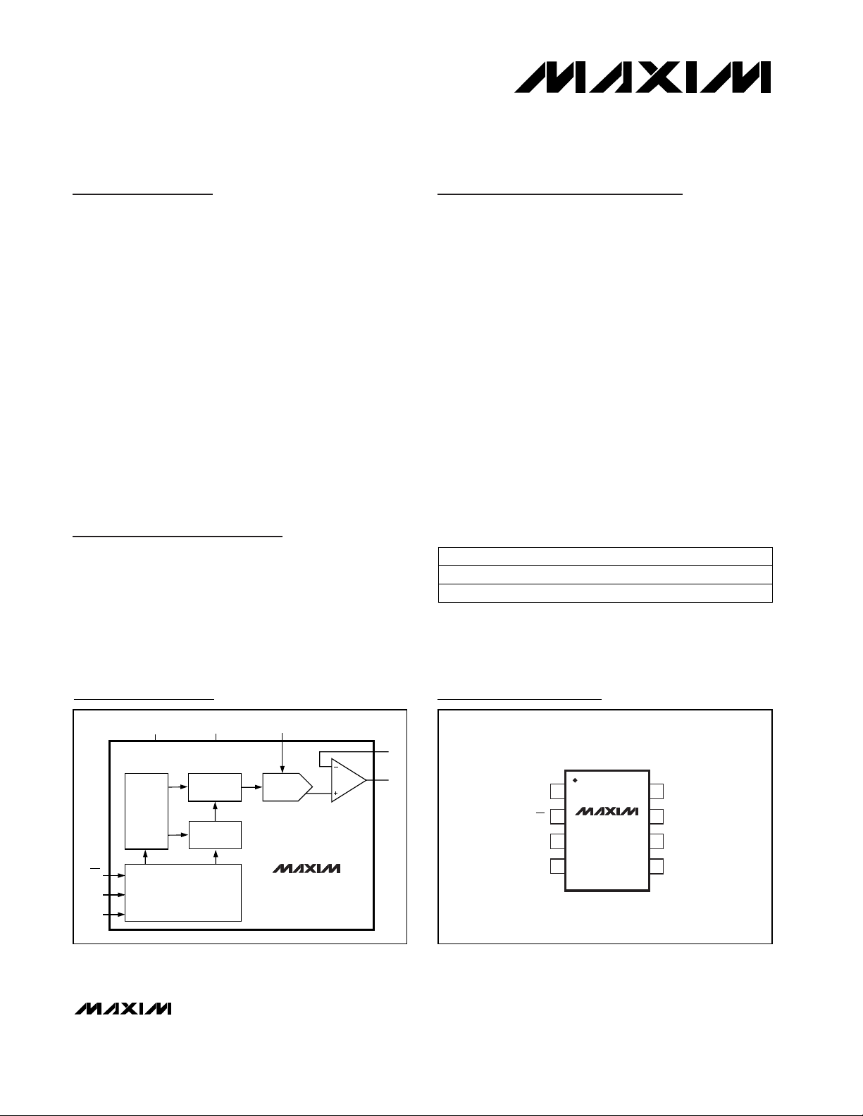
The MAX5304 combines a low-power, voltage-output,
10-bit digital-to-analog converter (DAC) and a precision
output amplifier in an 8-pin µMAX package. It operates
from a single +5V supply, drawing less than 280µA of
supply current.
The output amplifier’s inverting input is available to the
user, allowing specific gain configurations, remote
sensing, and high output-current capability. This makes
the MAX5304 ideal for a wide range of applications,
including industrial process control. Other features
include a software shutdown and power-on reset.
The serial interface is SPI™/QSPI™/MICROWIRE™
compatible. The DAC has a double-buffered input,
organized as an input register followed by a DAC register. A 16-bit serial word loads data into the input register. The DAC register can be updated independently or
simultaneously with the input register. All logic inputs
are TTL/CMOS-logic compatible and buffered with
Schmitt triggers to allow direct interfacing to optocouplers.
Applications
Digital Offset and Gain Adjustment
Industrial Process Control
Microprocessor-Controlled Systems
Portable Test Instruments
Remote Industrial Control
Features
♦ 10-Bit DAC with Configurable Output Amplifier
♦ +5V Single-Supply Operation
♦ Low Supply Current
0.28mA Normal Operation
2µA Shutdown Mode
♦ Available in 8-Pin µMAX
♦ Power-On Reset Clears DAC Output to Zero
♦ SPI/QSPI/MICROWIRE Compatible
♦ Schmitt-Trigger Digital Inputs for Direct
Optocoupler Interface
MAX5304
10-Bit Voltage-Output DAC
in 8-Pin µMAX
________________________________________________________________ Maxim Integrated Products 1
Functional Diagram
REF
DIN
FB
SCLK
1
2
8
7
V
DD
GND
CS
OUT
MAX5304
µMAX
TOP VIEW
3
4
6
5
Pin Configuration
19-1562; Rev 0; 10/99
PART
MAX5304CUA
MAX5304EUA -40°C to +85°C
0°C to +70°C
TEMP. RANGE PIN-PACKAGE
8 µMAX
8 µMAX
_________________Ordering Information
SPI and QSPI are trademarks of Motorola, Inc.
MICROWIRE is a trademark of National Semiconductor Corp.
For free samples & the latest literature: http://www.maxim-ic.com, or phone 1-800-998-8800.
For small orders, phone 1-800-835-8769.
V
GND
CONTROL
CS
DIN
SCLK
REGISTER
DD
DAC
REGISTER
INPUT
REGISTER
16-BIT
SHIFT
REF
FB
OUT
DAC
MAX5304

MAX5304
10-Bit Voltage-Output DAC
in 8-Pin µMAX
2 _______________________________________________________________________________________
ABSOLUTE MAXIMUM RATINGS
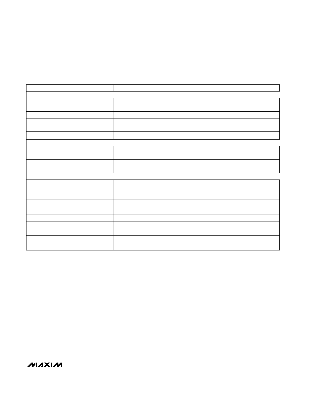
ELECTRICAL CHARACTERISTICS
(Circuit of Figure 8, VDD= +5V ±10%, V
REF
= +2.5V, RL= 5kΩ, CL= 100pF, TA= T
MIN
to T
MAX
, unless otherwise noted. Typical values
are at T
A
= +25°C. Output buffer connected in unity-gain configuration.)
Stresses beyond those listed under “Absolute Maximum Ratings” may cause permanent damage to the device. These are stress ratings only, and functional
operation of the device at these or any other conditions beyond those indicated in the operational sections of the specifications is not implied. Exposure to
absolute maximum rating conditions for extended periods may affect device reliability.
V
DD
to GND...............................................................-0.3V to +6V
REF, OUT, FB to GND.................................-0.3V to (V
DD
+ 0.3V)
Digital Inputs to GND................................................-0.3V to +6V
Continuous Current into Any Pin.......................................±20mA
Continuous Power Dissipation (T
A
= +70°C)
8-Pin µMAX (derate 4.10mW/°C above+70°C) ..........330mW
Operating Temperature Ranges
MAX5304CUA...................................................0°C to +70°C
MAX5304EUA ................................................-40°C to +85°C
Junction Temperature......................................................+150°C
Storage Temperature Range.............................-65°C to +150°C
Lead Temperature (soldering, 10s)........................... ......+300°C
Code dependent, minimum at code 1550 hex
4.5V ≤ VDD≤ 5.5V
Guaranteed monotonic
CONDITIONS
kΩ18 30R
REF
Reference Input Resistance
V0V
DD
- 1.4V
REF
Reference Input Range
µV/VPSRRPower-Supply Rejection Ratio 800
Bits10NResolution
ppm/°C1Gain-Error Tempco
LSBGEGain Error (Note 1) -0.3 ±2
ppm/°C6TCV
OS
Offset-Error Tempco
LSBDNLDifferential Nonlinearity ±1.0
±0.3 ±8 mVV
OS
Offset Error
UNITSMIN TYP MAXSYMBOLPARAMETER
LSB±4INL
Integral Nonlinearity
(Note 1)
V
REF
= 0.67Vp-p kHz650Reference -3dB Bandwidth
Input code = all 0s, V
REF
= 3.6Vp-p at 1kHz
V
REF
= 1Vp-p at 25kHz, code = full scale dB77SINAD
Signal-to-Noise Plus
Distortion Ratio
dB-84Reference Feedthrough
V2.4V
IH
Input High Voltage
VIN= 0 or V
DD
pF8C
IN
Input Capacitance
µA0.001 ±0.5I
IN
Input Leakage Current
V0.8V
IL
Input Low Voltage
STATIC PERFORMANCE—ANALOG SECTION
DIGITAL INPUTS
REFERENCE INPUT
MULTIPLYING-MODE PERFORMANCE

MAX5304
10-Bit Voltage-Output DAC
in 8-Pin µMAX
_______________________________________________________________________________________ 3
ELECTRICAL CHARACTERISTICS (continued)
(Circuit of Figure 8, VDD= +5V ±10%, V
REF
= +2.5V, RL= 5kΩ, CL= 100pF, TA= T
MIN
to T
MAX
, unless otherwise noted. Typical values
are at T
A
= +25°C. Output buffer connected in unity-gain configuration.)
(Note 3)
CS = VDD, DIN = 100kHz
Rail-to-rail (Note 2)
To ±1/2LSB, V
STEP
= 2.5V
CONDITIONS
mA0.28 0.4I
DD
Supply Current
V4.5 5.5V
DD
Supply Voltage
nVs5Digital Feedthrough
µs20Start-Up Time
µA0.001 ±0.1Current into FB
V0 to V
DD
Output Voltage Swing
µs10Output Settling Time
V/µs0.6SRVoltage Output Slew Rate
UNITSMIN TYP MAXSYMBOLPARAMETER
(Note 3) µA420Supply Current in Shutdown
µA0.001 ±0.5Reference Current in Shutdown
ns40t
CH
SCLK Pulse Width High
ns100t
CP
SCLK Clock Period
ns40t
CSS
CS Fall to SCLK Rise Setup Time
ns40t
DS
DIN Setup Time
ns0t
CSH
SCLK Rise to CS Rise Hold Time
ns40t
CL
SCLK Pulse Width Low
ns40t
CS1
CS Rise to SCLK Rise Hold Time
ns100t
CSW
CS Pulse Width High
ns40t
CS0
SCLK Rise to CS Fall Delay
ns0t
DH
DIN Hold Time
Note 1: Guaranteed from code 3 to code 1023 in unity-gain configuration.
Note 2: Accuracy is better than 1LSB for V
OUT
= 8mV to (VDD- 100mV), guaranteed by a power-supply rejection test at the end
points.
Note 3: R
L
= ∞, digital inputs at GND or VDD.
DIGITAL INPUTSDYNAMIC PERFORMANCE
POWER SUPPLIES
TIMING CHARACTERISTICS (Figure 6)

MAX5304
10-Bit Voltage-Output DAC
in 8-Pin µMAX
4 _______________________________________________________________________________________
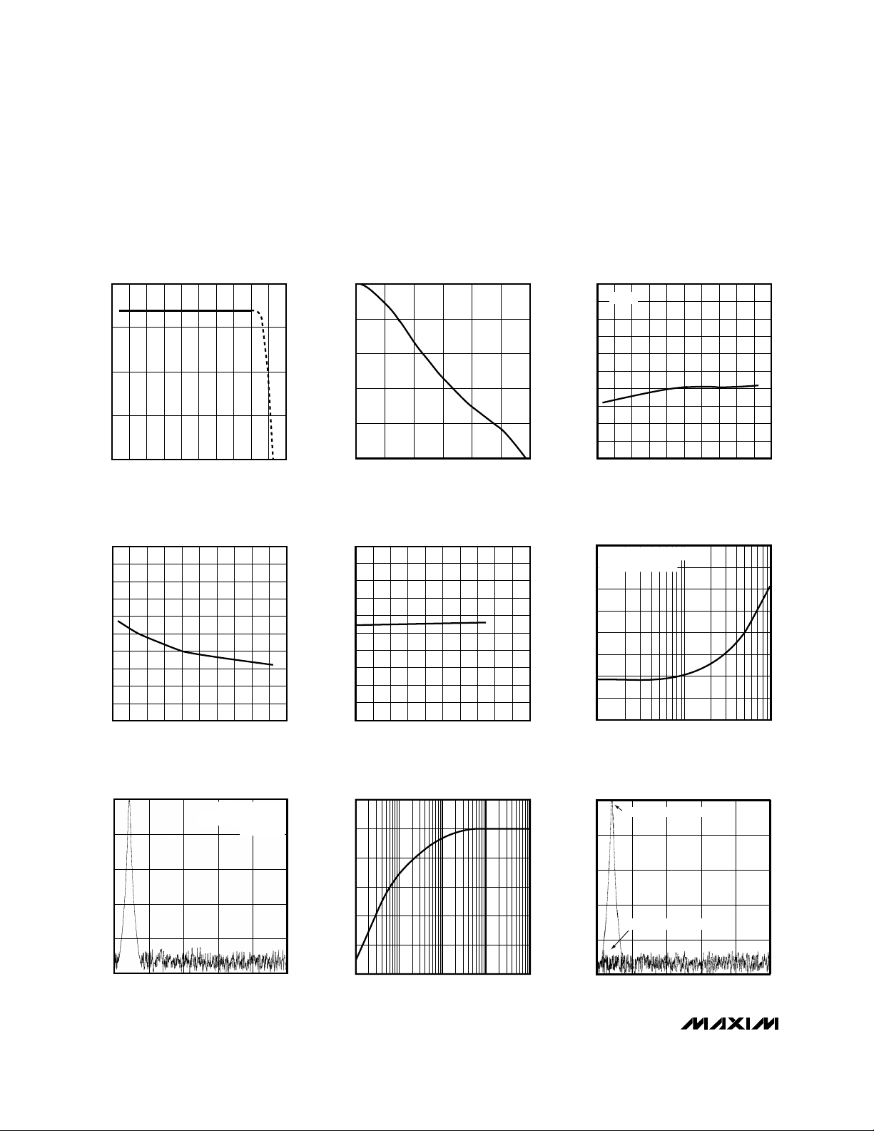
__________________________________________Typical Operating Characteristics
(VDD= +5V, RL= 5kΩ, CL= 100pF, TA = +25°C, unless otherwise noted.)
INL (LSB)
-0.050
0.4 1.2 2.0 2.8 3.6
REFERENCE VOLTAGE (V)
MAX5304-01
4.4
0.050
0.025
0
-0.025
INTEGRAL NONLINEARITY
vs. REFERENCE VOLTAGE
0
-4
-8
-12
-16
-20
500k0
1M 1.5M
2M 2.5M 3M
MAX5304-02
RELATIVE OUTPUT (dB)
REFERENCE VOLTAGE INPUT
FREQUENCY RESPONSE
FREQUENCY (Hz)
400
380
360
340
320
300
280
260
240
220
200
-60 -20 20 60 100 140
MAX5304-03
SUPPLY CURRENT (µA)
SUPPLY CURRENT
vs. TEMPERATURE
TEMPERATURE (°C)
RL = ∞
10
9
8
7
6
5
4
3
2
1
0
-60 -20 20 60 100 140
MAX5304-04
POWER-DOWN SUPPLY CURRENT (µA)
POWER-DOWN SUPPLY CURRENT
vs. TEMPERATURE
TEMPERATURE (°C)
-100
0.5 1.6 3.8
OUTPUT FFT PLOT
-60
0
MAX5304-07
FREQUENCY (kHz)
SIGNAL AMPLITUDE (dB)
2.7 4.9 6.0
-20
-40
-80
V
REF
= +3.6Vp-p
CODE = FULL SCALE
f
IN
= 1kHz
4.0 4.4 4.8 6.05.2 5.6
SUPPLY CURRENT
vs. SUPPLY VOLTAGE
MAX5304-05
SUPPLY VOLTAGE (V)
SUPPLY CURRENT (µA)
400
350
500
450
300
250
150
100
200
50
0
-50
-90
1
100
TOTAL HARMONIC DISTORTION
PLUS NOISE vs. FREQUENCY
-85
MAX5304-06
FREQUENCY (kHz)
THD + NOISE (dB)
-70
-60
10
-55
-80
-75
-65
V
REF
= +2.5VDC + 1Vp-p SINE
CODE = FULL SCALE
2.49956
2.49960
2.49964
2.49968
2.49972
2.49976
2.49980
0.1k 1k 10k 1M100k
OUTPUT VOLTAGE
vs. LOAD
MAX5304-08
LOAD (Ω)
OUTPUT VOLTAGE (V)
-100
0.5 1.6 3.8
REFERENCE FEEDTHROUGH
AT 1kHz
-60
0
MAX5304-09a/09b
FREQUENCY (kHz)
SIGNAL AMPLITUDE (dB)
2.7 4.9 6.0
-20
-40
-80
OUTPUT FEEDTHROUGH
REFERENCE INPUT SIGNAL
 Loading...