

Page 1
General Description
The MAX5290–MAX5295 dual, 12-/10-/8-bit, voltageoutput digital-to-analog converters (DACs) offer
buffered outputs and a 3µs maximum settling time at
the 12-bit level. The DACs operate from a 2.7V to 5.25V
analog supply and a separate 1.8V to 3.6V digital supply. The 20MHz 3-wire serial interface is compatible
with SPI™, QSPI™, MICROWIRE™, and digital signal
processor (DSP) protocol applications. Multiple devices
can share a common serial interface in direct access or
daisy-chained configuration. The MAX5290–MAX5295
provide two multifunctional, user-programmable, digital
I/O ports. The externally selectable power-up states of
the DAC outputs are either zero scale, midscale, or full
scale. Software-selectable FAST and SLOW settling
modes decrease settling time in FAST mode, or reduce
supply current in SLOW mode.
The MAX5290/MAX5291 are 12-bit DACs, the MAX5292/
MAX5293 are 10-bit DACs, and the MAX5294/MAX5295
are 8-bit DACs. The MAX5290/ MAX5292/MAX5294 provide unity-gain-configured output buffers, while the
MAX5291/MAX5293/MAX5295 provide force-sense-configured output buffers. The MAX5290– MAX5295 are
specified over the extended -40°C to +85°C temperature
range, and are available in space-saving 4mm x 4mm,
16-pin thin QFN and 6.5mm x 5mm, 14-pin and 16-pin
TSSOP packages.
Applications
Portable Instrumentation
Automatic Test Equipment (ATE)
Digital Offset and Gain Adjustment
Automatic Tuning
Programmable Voltage and Current Sources
Programmable Attenuators
Industrial Process Controls
Motion Control
Microprocessor (µP)-Controlled Systems
Power Amplifier Control
Fast Parallel-DAC to Serial-DAC Upgrades
Features
♦ Dual, 12-/10-/8-Bit Serial DACs in 4mm x 4mm
Thin QFN and TSSOP Packages
♦ 3µs (max) 12-Bit Settling Time to 1/2 LSB
♦ Integral Nonlinearity
1 LSB (max) MAX5290/MAX5291 A-Grade (12-Bit)
1 LSB (max) MAX5292/MAX5293 (10-Bit)
1/2 LSB (max) MAX5294/MAX5295 (8-Bit)
♦ Guaranteed Monotonic, ±1 LSB (max) DNL
♦ Two User-Programmable Digital I/O Ports
♦ Single +2.7V to +5.25V Analog Supply
♦ +1.8V to AV
DD
Digital Supply
♦ 20MHz 3-Wire SPI-/QSPI-/MICROWIRE- and
DSP-Compatible Serial Interface
♦ Glitch-Free Outputs Power Up to Zero Scale,
Midscale or Full Scale
♦ Unity-Gain- or Force-Sense-Configured Output
Buffers
MAX5290–MAX5295
Buffered, Fast-Settling, Dual, 12-/10-/8-Bit,
Voltage-Output DACs
________________________________________________________________ Maxim Integrated Products 1
Ordering Information
19-3005; Rev 3; 7/07
For pricing, delivery, and ordering information, please contact Maxim Direct at 1-888-629-4642,
or visit Maxim’s website at www.maxim-ic.com.
*Future product—contact factory for availability. Specifications
are preliminary.
**EP = Exposed paddle.
Selector Guide and Pin Configurations appear at end of data
sheet.
SPI/QSPI are trademarks of Motorola, Inc.
MICROWIRE is a trademark of National Semiconductor Corp.
PART TEMP RANGE PIN-PACKAGE
MAX5290AEUD -40°C to +85°C 14 TSSOP
MAX5290BEUD -40°C to +85°C 14 TSSOP
MAX5290AETE* -40°C to +85°C 16 Thin QFN-EP**
MAX5290BETE* -40°C to +85°C 16 Thin QFN-EP**
MAX5291AEUE -40°C to +85°C 16 TSSOP
MAX5291BEUE -40°C to +85°C 16 TSSOP
MAX5291AETE* -40°C to +85°C 16 Thin QFN-EP**
MAX5291BETE* -40°C to +85°C 16 Thin QFN-EP**
MAX5292EUD -40°C to +85°C 14 TSSOP
MAX5292ETE* -40°C to +85°C 16 Thin QFN-EP**
MAX5293EUE -40°C to +85°C 16 TSSOP
MAX5293ETE* -40°C to +85°C 16 Thin QFN-EP**
MAX5294EUD -40°C to +85°C 14 TSSOP
MAX5294ETE* -40°C to +85°C 16 Thin QFN-EP**
MAX5295EUE -40°C to +85°C 16 TSSOP
MAX5295ETE* -40°C to +85°C 16 Thin QFN-EP**
Page 2
MAX5290–MAX5295
Buffered, Fast-Settling, Dual, 12-/10-/8-Bit,
Voltage-Output DACs
2 _______________________________________________________________________________________
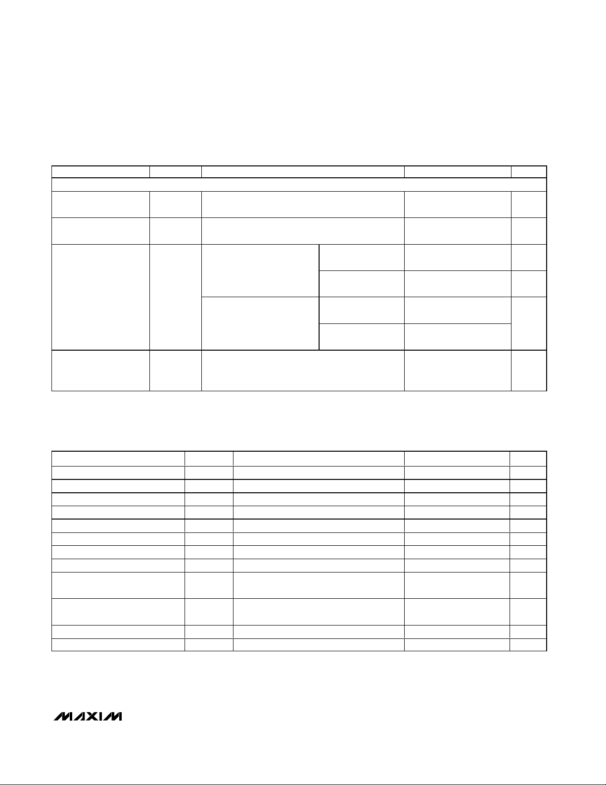
ABSOLUTE MAXIMUM RATINGS
ELECTRICAL CHARACTERISTICS
(AVDD= 2.7V to 5.25V, DVDD= 1.8V to AVDD, AGND = 0, DGND = 0, V
REF
= 2.5V, RL= 10kΩ, CL= 100pF, TA= T
MIN
to T
MAX
,
unless otherwise noted. Typical values are at T
A
= +25°C.) (Note 1)
Stresses beyond those listed under “Absolute Maximum Ratings” may cause permanent damage to the device. These are stress ratings only, and functional
operation of the device at these or any other conditions beyond those indicated in the operational sections of the specifications is not implied. Exposure to
absolute maximum rating conditions for extended periods may affect device reliability.
AVDDto DVDD........................................................................±6V
AGND to DGND ..................................................................±0.3V
AV
DD
to AGND, DGND.............................................-0.3V to +6V
DV
DD
to AGND, DGND ............................................-0.3V to +6V
FB_, OUT_,
REF to AGND........-0.3V to the lower of (AV
DD
+ 0.3V) or +6V
SCLK, DIN, CS, PU,
DSP to DGND.......-0.3V to the lower of (DV
DD
+ 0.3V) or +6V
UPIO1, UPIO2
to DGND ...............-0.3V to the lower of (DV
DD
+ 0.3V) or +6V
Maximum Current into Any Pin .........................................±50mA
Continuous Power Dissipation (T
A
= +70°C)
14-Pin TSSOP (derate 9.1mW/°C above +70°C) .........727mW
16-Pin TSSOP (derate 9.4mW/°C above +70°C) .........755mW
16-Pin Thin QFN (derate 16.9mW/°C above +70°C) .1349mW
Operating Temperature Range ...........................-40°C to +85°C
Storage Temperature Range .............................-65°C to +150°C
Maximum Junction Temperature .....................................+150°C
Lead Temperature (soldering, 10s) .................................+300°C
PARAMETER
CONDITIONS
UNITS
STATIC ACCURACY
MAX5290/MAX5291 12
MAX5292/MAX5293 10Resolution N
MAX5294/MAX5295 8
Bits
±1
±2 ±4
MAX5292/MAX5293 (10-bit)
±1
Integral Nonlinearity INL
V
REF
= 2.5V at
AV
DD
= 2.7V,
V
REF
= 4.096V
at AV
DD
= 5.25V
(Note 2)
MAX5294/MAX5295 (8-bit)
LSB
Differential Nonlinearity
DNL Guaranteed monotonic (Note 2) ±1 LSB
±5
±5
MAX5292/MAX5293 (10-bit), decimal code = 21 ±5
Offset Error V
OS
MAX5294/MAX5295 (8-bit), decimal code = 5 ±5
mV
Offset-Error Drift 5
ppm of
FS/°C
±4
MAX5292/MAX5293 (10-bit) ±3 ±5
Gain Error GE
MAX5294/MAX5295 (8-bit)
±2
LSB
Gain-Error Drift 1
ppm of
FS/°C
SYMBOL
MIN TYP MAX
MAX5290A/MAX5291A (12-bit)
MAX5290B/MAX5291B (12-bit)
MAX5290A/MAX5291A (12-bit), decimal code = 40
MAX5290B/MAX5291B (12-bit), decimal code = 82
MAX5290A/MAX5291A (12-bit)
Full-scale output
MAX5290B/MAX5291B (12-bit) ±10 ±20
±0.5
±0.125 ±0.5
±0.5
±25
±25
±25
Page 3
MAX5290–MAX5295
Buffered, Fast-Settling, Dual, 12-/10-/8-Bit,
Voltage-Output DACs
_______________________________________________________________________________________ 3
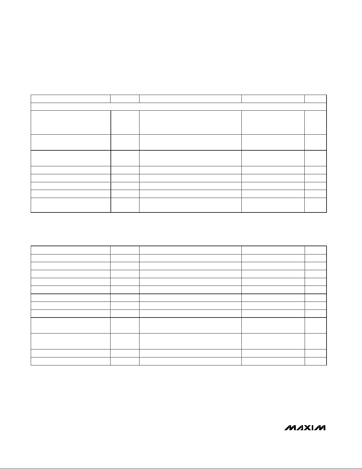
ELECTRICAL CHARACTERISTICS (continued)
(AVDD= 2.7V to 5.25V, DVDD= 1.8V to AVDD, AGND = 0, DGND = 0, V
REF
= 2.5V, RL= 10kΩ, CL= 100pF, TA= T
MIN
to T
MAX
,
unless otherwise noted. Typical values are at T
A
= +25°C.) (Note 1)
PARAMETER
CONDITIONS
Power-Supply Rejection
Ratio
PSRR Full-scale output, AV
DD
= 2.7V to 3.6V
REFERENCE INPUT
Reference Input Range
V
REF
V
Reference Input
Resistance
R
REF
Normal operation (no code dependence) 145
kΩ
Reference Leakage
Current
I
REF
Shutdown mode 0.5 1 µA
DAC OUTPUT CHARACTERISTICS
Unity gain 85
SLOW mode,
full scale
Force sense 67
Unity gain
Output Voltage Noise
FAST mode,
full scale
Force sense
Unity-gain output 0
Output Voltage Range
(Note 4)
Force-sense output 0
V
DC Output Impedance
38 Ω
Short-Circuit Current AVDD = 3V, OUT_ to AGND, full scale, FAST mode 45 mA
Power-Up Time From DVDD applied, interface is functional 30 60 µs
Wake-Up Time Coming out of shutdown, outputs settled 40 µs
Output OUT_ and FB_
Open-Circuit Leakage
Current
Programmed in shutdown mode, force-sense
outputs only
µA
DIGITAL OUTPUTS (UPIO_)
Output High Voltage V
OH
I
SOURCE
= 2mA
DV
DD
-
0.5
V
Output Low Voltage V
OL
I
SINK
= 2mA 0.4 V
DIGITAL INPUTS (SCLK, CS, DIN, DSP, UPIO_)
DVDD ≥ 2.7V 2.4
Input High Voltage V
IH
DVDD < 2.7V
0.7 x
V
DVDD > 3.6V 0.8
2.7V ≤ DVDD ≤ 3.6V 0.6
Input Low Voltage V
IL
DVDD < 2.7V 0.2
V
Input Leakage Current I
IN
±1 µA
Input Capacitance C
IN
10 pF
SYMBOL
MIN TYP MAX UNITS
0.25 AV
DV
DD
200 µV/V
200
140
110
0.01
±0.1
AV
AV
DD
DD
DD
/ 2
µV
RMS
Page 4
MAX5290–MAX5295
Buffered, Fast-Settling, Dual, 12-/10-/8-Bit,
Voltage-Output DACs
4 _______________________________________________________________________________________
ELECTRICAL CHARACTERISTICS (continued)
(AVDD= 2.7V to 5.25V, DVDD= 1.8V to AVDD, AGND = 0, DGND = 0, V
REF
= 2.5V, RL= 10kΩ, CL= 100pF, TA= T
MIN
to T
MAX
,
unless otherwise noted. Typical values are at T
A
= +25°C.) (Note 1)
PARAMETER
CONDITIONS
UNITS
PU INPUT
Input High Voltage V
IH-PU
DVDD -
V
Input Low Voltage V
IL-PU
200 mV
Input Leakage Current I
IN-PU
PU still considered floating when connected to a
tri-state bus
nA
DYNAMIC PERFORMANCE
Fast mode 3.6
Voltage-Output Slew
Rate
SR
Slow mode 1.6
V/µs
M AX 5290/M AX 5291 fr om cod e 322 to
cod e 4095 to 1/2 LS B
23
M AX 5292/M AX 5293 fr om cod e 82 to
cod e 1023 to 1/2 LS B
1.5 3
MAX5294/MAX5295 from code 21 to
code 255 to 1/2 LSB
12
M AX 5290/M AX 5291 fr om cod e 322 to
cod e 4095 to 1/2 LS B
36
MAX5292/MAX5293 from code 82 to
code 1023 to 1/2 LSB
2.5 6
Voltage-Output Settling
Time (Note 5)
MAX5294/MAX5295 from code 21 to
code 255 to 1/2 LSB
24
µs
FB_ Input Voltage 0
V
FB_ Input Current 0.1 µA
Unity gain 200
Reference -3dB
Bandwidth (Note 6)
Force sense 150
kHz
Digital Feedthrough
CS = DV
DD
, code = zero scale, any digital input
from 0 to DV
DD
and DVDD to 0, f = 100kHz
0.1
nV-s
Digital-to-Analog Glitch
Impulse
Major carry transition 2
nV-s
(Note 3) 15
nV-s
SYMBOL
MIN TYP MAX
200mV
±200
DAC-to-DAC Crosstalk
FAST mode
SLOW mode
V
REF
/ 2
Page 5
MAX5290–MAX5295
Buffered, Fast-Settling, Dual, 12-/10-/8-Bit,
Voltage-Output DACs
_______________________________________________________________________________________ 5
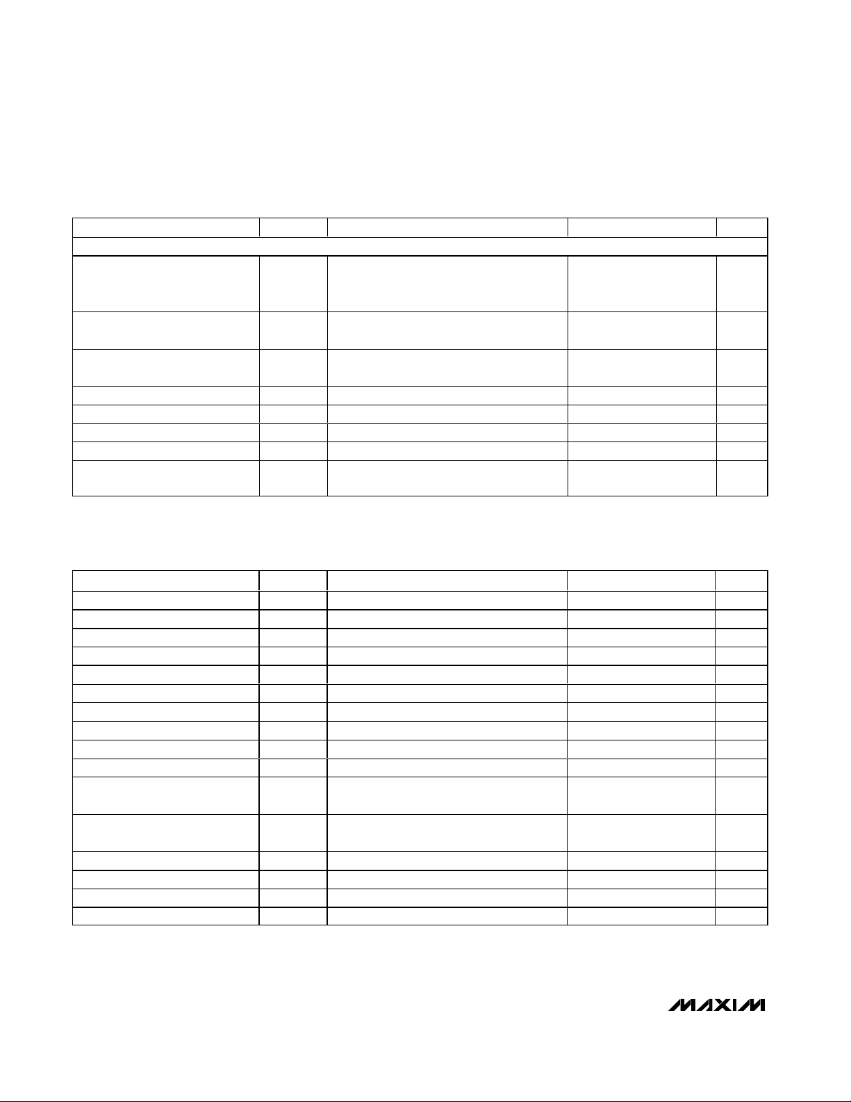
ELECTRICAL CHARACTERISTICS (continued)
(AVDD= 2.7V to 5.25V, DVDD= 1.8V to AVDD, AGND = 0, DGND = 0, V
REF
= 2.5V, RL= 10kΩ, CL= 100pF, TA= T
MIN
to T
MAX
,
unless otherwise noted. Typical values are at T
A
= +25°C.) (Note 1)
PARAMETER
SYMBOL
CONDITIONS
MIN
TYP
MAX
UNITS
POWER REQUIREMENTS
Analog Supply Voltage
Range
AV
DD
V
Digital Supply Voltage
Range
DV
DD
1.8
V
Unity gain
0.8 mA
SLOW mode, all digital inputs
at DGND or DV
DD
, no load,
V
REF
= 2.5V
Force sense 0.9 1.2 mA
Unity gain
2
Operating Supply
Current
I
AVDD
+
I
DVDD
FAST mode, all digital inputs
at DGND or DV
DD
, no load,
V
REF
= 2.5V
Force sense 1.2 2
mA
Shutdown Supply
Current
I
AV D D ( S H D N )
+
No clocks, all digital inputs at DGND or DVDD, all
DACs in shutdown mode
0.5 1.0 µA
TIMING CHARACTERISTICS—DSP Mode Disabled (3V, 3.3V Logic) (Figure 1)
(DVDD= 2.7V to 5.25V, DGND = 0, TA= T
MIN
to T
MAX
, unless otherwise noted.)
PARAMETER
CONDITIONS
UNITS
SCLK Frequency f
SCLK
2.7V < DVDD < 5.25V 20
MHz
SCLK Pulse-Width High t
CH
(Note 7) 20 ns
SCLK Pulse-Width Low t
CL
(Note 7) 20 ns
CS Fall to SCLK Rise Setup Time
t
CSS
10 ns
SCLK Rise to CS Rise Hold Time
t
CSH
5ns
SCLK Rise to CS Fall Setup Time
t
CS0
10 ns
DIN to SCLK Rise Setup Time t
DS
12 ns
DIN to SCLK Rise Hold Time t
DH
5ns
SCLK Rise to DOUTDC1 Valid
Propagation Delay
t
DO1
CL = 20pF, UPIO_ = DOUTDC1 mode 30 ns
SCLK Fall to DOUT_ Valid
Propagation Delay
t
DO2
CL = 20pF, UPIO_ = DOUTDC0 or DOUTRB
mode
30 ns
CS Rise to SCLK Rise Hold Time
t
CS1
MICROWIRE and SPI modes 0 and 3 10 ns
CS Pulse-Width High t
CSW
45 ns
I
D V D D ( S H D N )
2.70 5.25
0.55
0.85
AV
DD
SYMBOL
MIN TYP MAX
Page 6
MAX5290–MAX5295
Buffered, Fast-Settling, Dual, 12-/10-/8-Bit,
Voltage-Output DACs
6 _______________________________________________________________________________________
TIMING CHARACTERISTICS—DSP Mode Disabled (3V, 3.3V Logic) (Figure 1) (continued)
(DVDD= 2.7V to 5.25V, DGND = 0, TA= T
MIN
to T
MAX
, unless otherwise noted.)
PARAMETER
SYMBOL
CONDITIONS
MIN
TYP
MAX
UNITS
UPIO TIMING CHARACTERISTICS
DOUT Tri-State Time when Exiting
DOUTDC0, DOUTDC1, or
DOUTRB UPIO Modes
t
DOZ
CL = 20pF, from end of write cycle to UPIO_
in high impedance
100 ns
DOUTRB Tri-State Time from CS
Rise
t
DRBZ
CL = 20pF, from rising edge of CS to UPIO_
in high impedance
20 ns
DOUTRB Tri-State Enable Time
from 8th SCLK Rise
t
ZEN
CL = 20pF, from 8th rising edge of SCLK to
UPIO_ driven out of tri-state
0ns
LDAC Pulse-Width Low t
LDL
Figure 5 20 ns
LDAC Effective Delay t
LDS
Figure 6 100 ns
CLR, MID, SET Pulse-Width Low t
CMS
Figure 5 20 ns
GPO Output Settling Time t
GP
Figure 6 100 ns
GPO Output High-Impedance
Time
t
GPZ
100 ns
TIMING CHARACTERISTICS—DSP Mode Disabled (1.8V Logic) (Figure 1)
(DVDD= 1.8V to 5.25V, DGND = 0, TA= T
MIN
to T
MAX
, unless otherwise noted.)
PARAMETER
SYMBOL
CONDITIONS
MIN
TYP
MAX
UNITS
SCLK Frequency f
SCLK
1.8V < DVDD < 5.25V 10
MHz
SCLK Pulse-Width High t
CH
(Note 7) 40 ns
SCLK Pulse-Width Low t
CL
(Note 7) 40 ns
CS Fall to SCLK Rise Setup Time
t
CSS
20 ns
SCLK Rise to CS Rise Hold Time
t
CSH
0ns
SCLK Rise to CS Fall Setup Time
t
CS0
10 ns
DIN to SCLK Rise Setup Time t
DS
20 ns
DIN to SCLK Rise Hold Time t
DH
5ns
SCLK Rise to DOUTDC1 Valid
Propagation Delay
t
DO1
CL = 20pF, UPIO_ = DOUTDC1 mode 60 ns
SCLK Fall to DOUT_ Valid
Propagation Delay
t
DO2
CL = 20pF, UPIO_ = DOUTDC0 or DOUTRB
mode
60 ns
CS Rise to SCLK Rise Hold Time
t
CS1
MICROWIRE and SPI modes 0 and 3 20 ns
CS Pulse-Width High t
CSW
90 ns
Page 7
MAX5290–MAX5295
Buffered, Fast-Settling, Dual, 12-/10-/8-Bit,
Voltage-Output DACs
_______________________________________________________________________________________ 7
TIMING CHARACTERISTICS—DSP Mode Disabled (1.8V Logic) (Figure 1) (continued)
(DVDD= 1.8V to 5.25V, DGND = 0, TA= T
MIN
to T
MAX
, unless otherwise noted.)
PARAMETER
CONDITIONS
UNITS
UPIO_ TIMING CHARACTERISTICS
DOUT Tri-State Time when
Exiting DOUTDC0, DOUTDC1, or
DOUTRB UPIO Modes
t
DOZ
CL = 20pF, from end of write cycle to UPIO_
in high impedance
200 ns
DOUTRB Tri-State Time from CS
Rise
t
DRBZ
CL = 20pF, from rising edge of CS to UPIO_
in high impedance
40 ns
DOUTRB Tri-State Enable Time
from 8th SCLK Rise
t
ZEN
CL = 20pF, from 8th rising edge of SCLK to
UPIO_ driven out of tri-state
0ns
LDAC Pulse-Width Low t
LDL
Figure 5 40 ns
LDAC Effective Delay t
LDS
Figure 6 200 ns
CLR, MID, SET Pulse-Width Low
t
CMS
Figure 5 40 ns
GPO Output Settling Time t
GP
Figure 6 200 ns
GPO Output High-Impedance
Time
t
GPZ
200 ns
TIMING CHARACTERISTICS—DSP Mode Enabled (3V, 3.3V Logic) (Figure 2)
(DVDD= 2.7V to 5.25V, DGND = 0, TA= T
MIN
to T
MAX
, unless otherwise noted.)
PARAMETER
CONDITIONS
UNITS
SCLK Frequency f
SCLK
2.7V < DVDD < 5.25V 20
MHz
SCLK Pulse-Width High t
CH
(Note 7) 20 ns
SCLK Pulse-Width Low t
CL
(Note 7) 20 ns
CS Fall to SCLK Fall Setup Time t
CSS
10 ns
DSP Fall to SCLK Fall Setup Time
t
DSS
10 ns
SCLK Fall to CS Rise Hold Time t
CSH
5ns
SCLK Fall to CS Fall Delay t
CS0
10 ns
SCLK Fall to DSP Fall Delay t
DS0
10 ns
DIN to SCLK Fall Setup Time t
DS
12 ns
DIN to SCLK Fall Hold Time t
DH
5ns
SCLK Rise to DOUT_ Valid
Propagation Delay
t
DO1
CL = 20pF, UPIO_ = DOUTDC1 or DOUTRB
mode
30 ns
SCLK Fall to DOUTDC0 Valid
Propagation Delay
t
DO2
CL = 20pF, UPIO_ = DOUTDC0 mode 30 ns
CS Rise to SCLK Fall Hold Time t
CS1
MICROWIRE and SPI modes 0 and 3 10 ns
CS Pulse-Width High t
CSW
45 ns
DSP Pulse-Width High t
DSW
20 ns
DSP Pulse-Width Low t
DSPWL
(Note 8) 20 ns
SYMBOL
MIN TYP MAX
SYMBOL
MIN TYP MAX
Page 8
MAX5290–MAX5295
Buffered, Fast-Settling, Dual, 12-/10-/8-Bit,
Voltage-Output DACs
8 _______________________________________________________________________________________
TIMING CHARACTERISTICS—DSP Mode Enabled (3V, 3.3V Logic) (Figure 2) (continued)
(DVDD= 2.7V to 5.25V, DGND = 0, TA= T
MIN
to T
MAX
, unless otherwise noted.)
PARAMETER
SYMBOL
CONDITIONS
MIN
TYP
MAX
UNITS
UPIO_ TIMING CHARACTERISTICS
DOUT Tri-State Time when
Exiting DOUTDC0, DOUTDC1, or
DOUTRB UPIO Modes
t
DOZ
CL = 20pF, from end of write cycle to UPIO_
in high impedance
100 ns
DOUTRB Tri-State Time from CS
Rise
t
DRBZ
CL = 20pF, from rising edge of CS to UPIO_
in high impedance
20 ns
DOUTRB Tri-State Enable Time
from 8th SCLK Fall
t
ZEN
CL = 20pF, from 8th falling edge of SCLK to
UPIO_ driven out of tri-state
0ns
LDAC Pulse-Width Low t
LDL
Figure 5 20 ns
LDAC Effective Delay t
LDS
Figure 6
ns
CLR, MID, SET Pulse-Width Low
t
CMS
Figure 5 20 ns
GPO Output Settling Time t
GP
Figure 6 100 ns
GPO Output High-Impedance
Time
t
GPZ
100 ns
TIMING CHARACTERISTICS—DSP Mode Enabled (1.8V Logic) (Figure 2)
(DVDD= 1.8V to 5.25V, DGND = 0, TA= T
MIN
to T
MAX
, unless otherwise noted.)
PARAMETER
CONDITIONS
UNITS
SCLK Frequency f
SCLK
1.8V < DVDD < 5.25V 10
MHz
SCLK Pulse-Width High t
CH
(Note 7) 40 ns
SCLK Pulse-Width Low t
CL
(Note 7) 40 ns
CS Fall to SCLK Fall Setup Time t
CSS
20 ns
DSP Fall to SCLK Fall Setup Time
t
DSS
20 ns
SCLK Fall to CS Rise Hold Time t
CSH
0ns
SCLK Fall to CS Fall Delay t
CS0
10 ns
SCLK Fall to DSP Fall Delay t
DS0
15 ns
DIN to SCLK Fall Setup Time t
DS
20 ns
DIN to SCLK Fall Hold Time t
DH
5ns
SCLK Rise to DOUT_ Valid
Propagation Delay
t
DO1
CL = 20pF, UPIO_ = DOUTDC1 or DOUTRB
mode
60 ns
SCLK Fall to DOUTDC0 Valid
Propagation Delay
t
DO2
CL = 20pF, UPIO_ = DOUTDC0 mode 60 ns
CS Rise to SCLK Fall Hold Time t
CS1
MICROWIRE and SPI modes 0 and 3 20 ns
CS Pulse-Width High t
CSW
90 ns
DSP Pulse-Width High t
DSW
40 ns
DSP Pulse-Width Low
t
DSPWL
(Note 8)
40 ns
100
SYMBOL
MIN TYP MAX
Page 9
MAX5290–MAX5295
Buffered, Fast-Settling, Dual, 12-/10-/8-Bit,
Voltage-Output DACs
_______________________________________________________________________________________ 9
TIMING CHARACTERISTICS—DSP Mode Enabled (1.8V Logic) (Figure 2) (continued)
(DVDD= 1.8V to 5.25V, DGND = 0, TA= T
MIN
to T
MAX
, unless otherwise noted.)
PARAMETER
CONDITIONS
UNITS
UPIO_ TIMING CHARACTERISTICS
DOUT Tri-State Time when
Exiting DOUTDC0, DOUTDC1, or
DOUTRB UPIO_ Modes
t
DOZ
CL = 20pF, from end of write cycle to UPIO_
in high impedance
200 ns
DOUTRB Tri-State Time from CS
Rise
t
DRBZ
CL = 20pF, from rising edge of CS to UPIO_
in high impedance
40 ns
DOUTRB Tri-State Enable Time
from 8th SCLK Fall
t
ZEN
CL = 20pF, from 8th falling edge of SCLK to
UPIO_ driven out of tri-state
0ns
LDAC Pulse-Width Low t
LDL
Figure 5 40 ns
LDAC Effective Delay t
LDS
Figure 6
ns
CLR, MID, SET Pulse-Width Low
t
CMS
Figure 5 40 ns
GPO Output Settling Time t
GP
Figure 6 200 ns
GPO Output High-Impedance
Time
t
GPZ
200 ns
Note 1: For the force-sense versions, FB_ is connected to its respective OUT_. V
OUT
(max) = V
REF
/ 2, unless otherwise noted.
Note 2: Linearity guaranteed from decimal code 40 to 4095 for the MAX5290A/MAX5291A (12-bit, A-grade), code 82 to 4095 for the
MAX5290B/MAX5291B (12-bit, B-grade), code 21 to 1023 for the MAX5292/MAX5293 (10-bit), and code 5 to 255 for the
MAX5294/MAX5295 (8-bit).
Note 3: DAC-to-DAC crosstalk is measured as follows: outputs of DACA and DACB are set to full scale and the output of DACB is
measured. While keeping DACB unchanged, the output of DACA is transitioned to zero scale and the ∆V
OUT
of DACB is
measured. The procedure is repeated with DACA and DACB interchanged. DAC-to-DAC crosstalk is the maximum ∆V
OUT
measured.
Note 4: Represents the functional range. The linearity is guaranteed at V
REF
= 2.5V. See the Typical Operating Characteristics sec-
tion for linearity at other voltages.
Note 5: Guaranteed by design.
Note 6: The reference -3dB bandwidth is measured with a 0.1V
P-P
sine wave on V
REF
and with the input code at full scale.
Note 7: In some daisy-chain modes, data is required to be clocked in on one clock edge and the shifted data clocked out on the fol-
lowing edge. In the case of a 1/2 clock-period delay, it is necessary to increase the minimum high/low clock times to 25ns
(2.7V) or 50ns (1.8V).
Note 8: The falling edge of DSP starts a DSP-type bus cycle, provided that CS is also active low to select the device. DSP active low
and CS active low must overlap by a minimum of 10ns (2.7V) or 20ns (1.8V). CS can be permanently low in this mode of
SYMBOL
MIN TYP MAX
200
Page 10
MAX5290–MAX5295
Buffered, Fast-Settling, Dual, 12-/10-/8-Bit,
Voltage-Output DACs
10 ______________________________________________________________________________________
Typical Operating Characteristics
(AVDD= DVDD= 3V, V
REF
= 2.5V, RL= 10kΩ, CL= 100pF, speed mode = FAST, PU = floating, TA= +25°C, unless otherwise noted.)
-0.8
-0.4
-0.6
0
-0.2
0.2
0.4
0 20001000 3000 4000 4096
INTEGRAL NONLINEARITY vs. DIGITAL
INPUT CODE (MAX5290A)
MAX5290 toc01
INPUT CODE
INL (LSB)
-0.35
-0.20
-0.25
-0.30
-0.15
-0.10
-0.05
0
0.05
0.10
0.15
0 20001000 3000 4000 4096
INTEGRAL NONLINEARITY vs. DIGITAL
INPUT CODE (MAX5291A)
MAX5290 toc02
INPUT CODE
INL (LSB)
INTEGRAL NONLINEARITY
vs. DIGITAL INPUT CODE (12-BIT)
MAX5290 toc03
DIGITAL INPUT CODE
INL (LSB)
307220481024
-3
-2
-1
0
1
2
3
4
-4
0 4096
UNITY GAIN
B-GRADE
INTEGRAL NONLINEARITY
vs. DIGITAL INPUT CODE (10-BIT)
MAX5290 toc04
DIGITAL INPUT CODE
INL (LSB)
768512256
-0.75
-0.50
-0.25
0
0.25
0.50
0.75
1.00
-1.00
01024
UNITY GAIN
INTEGRAL NONLINEARITY
vs. DIGITAL INPUT CODE (8-BIT)
MAX5290 toc05
DIGITAL INPUT CODE
INL (LSB)
19212864
-0.25
0
0.25
0.50
-0.50
0256
UNITY GAIN
DIFFERENTIAL NONLINEARITY
vs. DIGITAL INPUT CODE (12-BIT)
MAX5290 toc06
DIGITAL INPUT CODE
DNL (LSB)
307220481024
-0.1
0
0.1
0.2
-0.2
0 4096
UNITY GAIN
DIFFERENTIAL NONLINEARITY
vs. DIGITAL INPUT CODE (10-BIT)
MAX5290 toc07
DIGITAL INPUT CODE
DNL (LSB)
768512256
-0.025
0
0.025
0.050
-0.050
01024
UNITY GAIN
DIFFERENTIAL NONLINEARITY
vs. DIGITAL INPUT CODE (8-BIT)
MAX5290 toc08
DIGITAL INPUT CODE
DNL (LSB)
19212864
-0.01
0
0.01
0.02
-0.02
0256
UNITY GAIN
0
0.05
0.10
0.15
0.20
0.25
0.30
0.35
0.40
-40 -15 10 35 60 85
INTEGRAL NONLINEARITY
vs. TEMPERATURE (A-GRADE)
MAX5290 toc09
TEMPERATURE (°C)
INL (LSB)
UNITY GAIN
FORCE
SENSE
MIDSCALE
Page 11
MAX5290–MAX5295
Buffered, Fast-Settling, Dual, 12-/10-/8-Bit,
Voltage-Output DACs
______________________________________________________________________________________ 11
Typical Operating Characteristics (continued)
(AVDD= DVDD= 3V, V
REF
= 2.5V, RL= 10kΩ, CL= 100pF, speed mode = FAST, PU = floating, TA= +25°C, unless otherwise noted.)
INTEGRAL NONLINEARITY
vs. TEMPERATURE (12-BIT)
MAX5290 toc10
TEMPERATURE (°C)
INL (LSB)
603510-15
-2
0
2
4
-4
-40 85
UNITY GAIN
B-GRADE
DIFFERENTIAL NONLINEARITY
vs. TEMPERATURE (12-BIT)
MAX5290 toc11
TEMPERATURE (°C)
DNL (LSB)
603510-15
-0.1
0
0.1
0.2
-0.2
-40 85
UNITY GAIN
0
0.10
0.05
0.20
0.15
0.30
0.25
0.35
0.45
0.40
0.50
1.0 2.0 2.51.5 3.0 3.5 4.0 4.5 5.0
MAX5290 toc12
V
REF
(V)
INL (LSB)
INTEGRAL NONLINEARITY
vs. REFERENCE VOLTAGE (MAX5290A)
0
0.2
0.1
0.4
0.3
0.6
0.5
0.7
0.9
0.8
1.0
1.0 2.0 2.51.5 3.0 3.5 4.0 4.5 5.0
INTEGRAL NONLINEARITY
vs. REFERENCE VOLTAGE (MAX5291A)
MAX5290 toc13
V
REF
(V)
INL (LSB)
0
0.1
0.2
0.3
0.4
0.5
0.6
0.7
0.8
-40 -15 10 35 60 85
OFFSET ERROR vs. TEMPERATURE
(A-GRADE)
MAX5290 toc14
TEMPERATURE (°C)
OFFSET ERROR (mV)
UNITY GAIN
FORCE
SENSE
CODE = 40
UNITY GAIN: 1 LSB = 0.6mV
FORCE SENSE: 1 LSB = 0.3mV
OFFSET ERROR vs. TEMPERATURE
MAX5290 toc15
TEMPERATURE (°C)
OFFSET ERROR (LSB)
603510-15
-8
-6
-4
-2
0
-10
-40 85
FORCE SENSE
UNITY GAIN
UNITY GAIN: 1 LSB = 0.6mV
FORCE SENSE: 1 LSB = 0.3mV
-0.35
-0.20
-0.25
-0.30
-0.15
-0.10
-0.05
0
0.05
0.10
0.15
-40 10-15 356085
GAIN ERROR vs. TEMPERATURE
(A-GRADE)
MAX5290 toc16
TEMPERATURE (°C)
GAIN ERROR (LSB)
UNITY GAIN
FORCE
SENSE
UNITY GAIN: 1 LSB = 0.6mV
FORCE SENSE: 1 LSB = 0.3mV
GAIN ERROR vs. TEMPERATURE
MAX5290 toc17
TEMPERATURE (°C)
GAIN ERROR (LSB)
603510-15
-8
-6
-4
-2
0
-10
-40 85
FORCE SENSE
UNITY GAIN
UNITY GAIN: 1 LSB = 0.6mV
FORCE SENSE: 1 LSB = 0.3mV
REFERENCE INPUT BANDWIDTH
MAX5290 toc18
FREQUENCY (Hz)
GAIN (dB)
1M100k10k1k
-25
-20
-15
-10
-5
0
5
-30
010M
V
REF
= 0.1V
P-P
AT 2.5V
DC
Page 12

MAX5290–MAX5295
Buffered, Fast-Settling, Dual, 12-/10-/8-Bit,
Voltage-Output DACs
12 ______________________________________________________________________________________
Typical Operating Characteristics
(TA = +25°C, unless otherwise noted.)
0.4
0.7
0.6
0.5
0.8
0.9
1.1
1.0
1.2
0 1024 2048 3072 4096
SUPPLY CURRENT vs. DIGITAL
INPUT CODE (FORCE SENSE)
MAX5290 toc19
DIGITAL INPUT CODE
SUPPLY CURRENT (mA)
SLOW MODE
12-BIT
NO LOAD
0.3
0.2
0.1
0
0
0.1
0.2
0.3
0.4
0.5
0.6
0.7
0.8
0 1024 2048 3072 4096
SUPPLY CURRENT vs. DIGITAL
INPUT CODE (UNITY GAIN)
MAX5290 toc20
DIGITAL INPUT CODE
SUPPLY CURRENT (mA)
SLOW MODE
12-BIT
NO LOAD
0.4
0.7
0.6
0.5
0.9
0.8
1.3
1.2
1.1
1.0
1.4
2.7 3.1 3.5 3.9 4.3 4.7 5.1 5.5
SUPPLY CURRENT vs. SUPPLY
VOLTAGE (FORCE SENSE)
MAX5290 toc21
SUPPLY VOLTAGE (V)
SUPPLY CURRENT (mA)
FAST MODE
I = I
AVDD
+ I
DVDD
AVDD = DV
DD
NO LOAD
SLOW MODE
0
0.3
0.2
0.1
0.5
0.4
0.9
0.8
0.7
0.6
1.0
2.7 3.1 3.5 3.9 4.3 4.7 5.1 5.5
SUPPLY CURRENT vs. SUPPLY
VOLTAGE (UNITY GAIN)
MAX5290 toc22
SUPPLY VOLTAGE (V)
SUPPLY CURRENT (mA)
FAST MODE
I = I
AVDD
+ I
DVDD
AVDD = DV
DD
NO LOAD
SLOW MODE
50
65
60
55
75
70
95
90
85
80
100
2.7 3.1 3.5 3.9 4.3 4.7 5.1 5.5
SHUTDOWN SUPPLY CURRENT
vs. SUPPLY VOLTAGE
MAX5290 toc23
SUPPLY VOLTAGE (V)
SHUTDOWN SUPPLY CURRENT (nA)
FORCE SENSE
AVDD = DV
DD
I = I
AVDD
+ I
DVDD
NO LOAD
UNITY GAIN
-5
-2
-3
-4
-1
0
1
2
3
4
5
-40 10-15 35 60 85
OFFSET ERROR vs. TEMPERATURE
MAX5290 toc24
TEMPERATURE (°C)
OFFSET ERROR (LSB)
FORCE SENSE
B-GRADE
UNITY GAIN: 1 LSB = 1mV
FORCE SENSE: 1 LSB = 0.5mV
UNITY GAIN
-5
-2
-3
-4
-1
0
1
2
3
4
5
-40 10-15 35 60 85
GAIN ERROR vs. TEMPERATURE
MAX5290 toc25
TEMPERATURE (°C)
GAIN ERROR (LSB)
FORCE SENSE
B-GRADE
UNITY GAIN: 1 LSB = 1mV
FORCE SENSE: 1 LSB = 0.5mV
UNITY GAIN
1.80
1.90
1.85
2.00
1.95
2.05
2.10
2.15
2.20
-40 -20 -10-30 0 10 20 30 40
OUTPUT VOLTAGE vs. OUTPUT
SOURCE/SINK CURRENT
MAX5290 toc26
I
OUT
(mA)
OUTPUT VOLTAGE (V)
MIDSCALE
UNITY GAIN
V
REF
= 4.096V
200ns/div
MAJOR-CARRY TRANSITION GLITCH
OUT_
(AC-COUPLED)
10mV/div
MAX5290 toc27
CS
2V/div
Page 13

MAX5290–MAX5295
Buffered, Fast-Settling, Dual, 12-/10-/8-Bit,
Voltage-Output DACs
______________________________________________________________________________________ 13
400ns/div
SETTLING TIME POSITIVE
OUT_
2V/div
MAX5290 toc28
CS
2V/div
FULL-SCALE TRANSITION
400ns/div
SETTLING TIME NEGATIVE
OUT_
2V/div
MAX5290 toc29
CS
2V/div
FULL-SCALE TRANSITION
REFERENCE INPUT BANDWIDTH
MAX5290 toc30
FREQUENCY (kHz)
GAIN (dB)
100010010
-20
-15
-10
-5
0
5
-25
1 10,000
V
REF
= 0.1V
P-P
AT 4.096V
DC
UNITY GAIN
REFERENCE FEEDTHROUGH AT 1kHz
MAX5290 toc31
FREQUENCY (kHz)
5.0
4.53.5 4.01.5 2.0 2.5 3.01.0
-110
-120
-130
-100
-90
-80
-70
-60
-50
-40
-30
-22
-142
0.5 5.5
100µs/div
DAC-TO-DAC CROSSTALK
OUTB
1mV/div
MAX5290 toc32
OUTA
2V/div
1µs/div
DIGITAL FEEDTHROUGH
OUT_
(AC-COUPLED)
10mV/div
MAX5290 toc33
SCLK
2V/div
20µs/div
POWER-UP GLITCH
AV
DD
2V/div
MAX5290 toc34
OUT_
1V/div
PU = FLOATING
10µs/div
EXITING SHUTDOWN TO MIDSCALE
OUT_
1V/div
MAX5290 toc35
UPIO_
2V/div
PU = FLOATING
Typical Operating Characteristics
(TA = +25°C, unless otherwise noted.)
Page 14

MAX5290–MAX5295
Buffered, Fast-Settling, Dual, 12-/10-/8-Bit,
Voltage-Output DACs
14 ______________________________________________________________________________________
Pin Description
PIN
MAX5290
MAX5292
MAX5294
MAX5291
MAX5293
MAX5295
THIN QFN
TSSOP
TSSOP
NAME FUNCTION
1213DSP
Clock Enable. Connect DSP to DV
DD
at power-up to transfer
data on the rising edge of SCLK. Connect DSP to DGND at
power-up to transfer data on the falling edge of SCLK.
2 3 2 4 DIN Serial Data Input
3435CS Active-Low Chip-Select Input
4 5 4 6 SCLK Serial Clock Input
5657DVDDDigital Supply
6 7 6 8 DGND Digital Ground
7 8 7 9 AGND Analog Ground
89810AVDDAnalog Supply
9 10 9 11 OUTB DACB Output
— — 10 12 FBB Feedback for DACB Output Buffer
10 11 11 13 REF Reference Input
— — 12 14 FBA Feedback for DACA Output Buffer
11, 13 — — — N.C. No Connection. Not internally connected.
12 12 13 15 OUTA DACA Output
14 13 14 16 PU
Power-Up State Select Input. Connect PU to DV
DD
to set OUTA
and OUTB to full scale upon power-up. Connect PU to DGND to
set OUTA and OUTB to zero upon power-up. Leave PU floating
to set OUTA and OUTB to midscale upon power-up.
15 14 15 1 UPIO2 User-Programmable Input/Output 2
16 1 16 2 UPIO1 User-Programmable Input/Output 1
————EP
Exposed Paddle (QFN Only). Not internally connected. Do not
connect to circuitry.
THIN QFN
Page 15

MAX5290–MAX5295
Buffered, Fast-Settling, Dual, 12-/10-/8-Bit,
Voltage-Output DACs
______________________________________________________________________________________ 15
Functional Diagrams
MAX5290
MAX5292
MAX5294
DOUT
REGISTER
16-BIT SHIFT
REGISTER
CS
SCLK
DIN
DSP
SERIAL
INTERFACE
CONTROL
MUX
AV
DD
UPIO1
UPIO2
REF
PU
UPIO1 AND
UPIO2
LOGIC
POWER-DOWN
LOGIC AND
REGISTER
DECODE
CONTROL
INPUT
REGISTER
DAC
REGISTER
DAC A
OUTA
INPUT
REGISTER
DAC B
OUTB
DAC
REGISTER
DV
DD
AGND DGND
Page 16

MAX5290–MAX5295
Buffered, Fast-Settling, Dual, 12-/10-/8-Bit,
Voltage-Output DACs
16 ______________________________________________________________________________________
Functional Diagrams (continued)
MAX5291
MAX5293
MAX5295
DOUT
REGISTER
16-BIT SHIFT
REGISTER
CS
SCLK
DIN
DSP
SERIAL
INTERFACE
CONTROL
MUX
AV
DD
UPIO1
UPIO2
REF
PU
UPIO1 AND
UPIO2
LOGIC
POWER-DOWN
LOGIC AND
REGISTER
DECODE
CONTROL
INPUT
REGISTER
DAC
REGISTER
DAC A
OUTA
FBA
INPUT
REGISTER
DAC B
OUTB
FBB
DAC
REGISTER
DV
DD
AGND DGND
Page 17

MAX5290–MAX5295
Buffered, Fast-Settling, Dual, 12-/10-/8-Bit,
Voltage-Output DACs
______________________________________________________________________________________ 17
Detailed Description
The MAX5290–MAX5295 dual, 12-/10-/8-bit, voltageoutput digital-to-analog converters (DACs) offer
buffered outputs and a 3µs maximum settling time at
the 12-bit level. The DACs operate from a single 2.7V to
5.25V analog supply and a separate 1.8V to AVDDdigital supply. The MAX5290–MAX5295 include an input
register and DAC register for each channel and a
16-bit data-in/data-out shift register. The 3-wire serial
interface is compatible with SPI, QSPI, MICROWIRE,
and DSP applications. The MAX5290–MAX5295 provide two user-programmable digital I/O ports, which
are programmed through the serial interface. The externally selectable power-up states of the DAC outputs
are either zero scale, midscale, or full scale.
Reference Input
The reference input, REF, accepts both AC and DC values with a voltage range extending from 0.25V to
AVDD. The voltage at REF (V
REF
) sets the full-scale output of the DACs. Determine the output voltage using
the following equation:
Unity-gain versions:
V
OUT_
= (V
REF
x CODE) / 2
N
Force-sense versions (FB_ connected to OUT_):
V
OUT
= 0.5 x (V
REF
x CODE) / 2
N
where CODE is the numeric value of the DAC’s binary
input code and N is the bits of resolution. For the
MAX5290/MAX5291, N = 12 and CODE ranges from 0
to 4095. For the MAX5292/MAX5293, N = 10 and
CODE ranges from 0 to 1023. For the MAX5294/
MAX5295, N = 8 and CODE ranges from 0 to 255.
Output Buffers
The DACA and DACB output-buffer amplifiers of the
MAX5290–MAX5295 are unity-gain stable with rail-torail output voltage swings and a typical slew rate of
5.7V/µs. The MAX5290/MAX5292/MAX5294 provide
unity-gain outputs, while the MAX5291/MAX5293/
MAX5295 provide force-sense outputs. For the
MAX5291/MAX5293/MAX5295, access to the output
amplifier’s inverting input provides flexibility in output
gain setting and signal conditioning (see the
Applications Information section).
The MAX5290–MAX5295 offer FAST and SLOW-settling
time modes. In the FAST mode, the settling time is 3µs
(max), and the supply current is 2mA (max). In the SLOW
mode, the settling time is 6µs (max), and the supply current drops to 0.8mA (max). See the Digital Interface section for settling-time mode programming details.
Use the serial interface to set the shutdown output
impedance of the amplifiers to 1kΩ or 100kΩ for the
MAX5290/MAX5292/MAX5294 and 1kΩ or high imped-
ance for the MAX5291/MAX5293/MAX5295. The DAC
outputs can drive a 2kΩ (typ) load and are stable with
up to 500pF (typ) of capacitive load.
Power-On Reset
At power-up, all DAC outputs power up to full scale,
midscale, or zero scale, depending on the configuration
of the PU input. Connect PU to DVDDto set OUT_ to full
scale upon power-up. Connect PU to DGND to set
OUT_ to zero scale upon power-up. Leave PU floating
to set OUT_ to midscale.
Digital Interface
The MAX5290–MAX5295 use a 3-wire serial interface
that is compatible with SPI, QSPI, MICROWIRE, and
DSPs (Figures 1 and 2). Connect DSP to DVDDbefore
power-up to clock data in on the rising edge of SCLK.
Connect DSP to DGND before power-up to clock data in
on the falling edge of SCLK. After power-up, the device
enters DSP frame sync mode on the first rising edge of
DSP. Refer to the Programmer’s Handbook for details.
Each MAX5290–MAX5295 includes a 16-bit input shift
register. The data is loaded into the input shift register
through the serial interface. The 16 bits can be sent in
two serial 8-bit packets or one 16-bit word (CS must
remain low until all 16 bits are transferred). The data is
loaded MSB first. For the MAX5290/MAX5291, the 16
bits consist of 4 control bits (C3–C0) and 12 data bits
(D11–D0) (see Table 1). For the 10-bit MAX5292/
MAX5293 devices, D11–D2 are the data bits and D1
and D0 are sub-bits. For the 8-bit MAX5294/
MAX5295 devices, D11–D4 are the data bits and
D3–D0 are sub-bits. Set all sub-bits to zero for optimum
performance.
Each DAC channel includes two registers: an input register and the DAC register. At power-up, the DAC output is set according to the state of PU. The DACs are
double-buffered, which allows any of the following for
each channel:
• Loading the input register without updating the DAC
register
• Loading the DAC register without updating the input
register
• Updating the DAC register from the input register
• Updating the input and DAC registers simultaneously
Page 18

MAX5290–MAX5295
Buffered, Fast-Settling, Dual, 12-/10-/8-Bit,
Voltage-Output DACs
18 ______________________________________________________________________________________
Table 1. Serial Write Data Format
MSB 16 BITS OF SERIAL DATA
LSB
CONTROL BITS DATA BITS
C3
D0
Figure 1. Serial-Interface Timing Diagram (DSP Mode Disabled)
Figure 2. Serial-Interface Timing Diagram (DSP Mode Enabled)
SCLK
DIN
CS
DOUTDC1*
DOUTDC0
OR
DOUTRB*
*UPIO1/UPIO2 CONFIGURED AS DOUTDC_ (DAISY-CHAIN DATA OUTPUT, MODE 0 OR 1) OR DOUTRB (READ-BACK DATA OUTPUT).
SEE THE DATA OUTPUT SECTION FOR DETAILS.
t
CH
t
DS
t
CS0
t
DH
t
CSH
t
DO1
t
DO2
t
CL
C2C3 C1 D0
t
CSW
t
CS1
DOUT VALID
DOUT VALID
t
CSS
C2 C1 C0 D11 D10 D9 D8 D7 D6 D5 D4 D3 D2 D1
SCLK
t
DS
DIN
t
CS0
CS
DSP
DOUTDC0*
DOUTDC1
OR
DOUTRB*
*UPIO1/UPIO2 CONFIGURED AS DOUTDC_ (DAISY-CHAIN DATA OUTPUT, MODE 0 OR 1) OR DOUTRB (READ-BACK DATA OUTPUT).
SEE THE DATA OUTPUT SECTION FOR DETAILS.
t
CSW
t
DSWtDSPWL
C3 C2 C1 D0
t
DH
t
CSS
t
DSS
t
DS0
t
D01
t
CL
t
D02
DOUT VALID
t
CH
DOUT VALID
t
CSH
t
CS1
Page 19

MAX5290–MAX5295
Buffered, Fast-Settling, Dual, 12-/10-/8-Bit,
Voltage-Output DACs
______________________________________________________________________________________ 19
SCLK
DIN
C3 C2 C1 C0 D11 D10 D9 D8 D7 D6 D5 D4 D3 D2 D1 D0
DIN
SCLK
DV
DD
COMMAND TAKES EFFECT HERE
ONLY IF SCLK COUNT = N
✕
16
COMMAND TAKES EFFECT HERE
ONLY IF SCLK COUNT = N
✕
16
MICROWIRE OR SPI (CPOL = 0, CPHA = 0) 8-BIT CONTROL DATA OR 12-BIT DAC DATA WRITE:
CS MUST REMAIN LOW BETWEEN BYTES ON A 16-BIT WRITE OPERATION
SPI (CPOL = 1, CPHA = 1) 8-BIT CONTROL DATA OR 12-BIT DAC DATA WRITE:
CS MUST REMAIN LOW BETWEEN BYTES ON A 16-BIT WRITE OPERATION
DIN
SCLK
CS
CS
MAX5290–
MAX5295
V
DD
V
DD
MICROWIRE
SK
SO
I/O
SCLK
DIN
DV
DD
MAX5290–
MAX5295
V
DD
V
DD
SPI OR QSPI
SCK
MOSI
SS OR I/O
CS
DSPDSP
CS
C3 C2 C1 C0 D11 D10 D9 D8 D7 D6 D5 D4 D3 D2 D1 D0
Figure 3. MICROWIRE and SPI (CPOL = 0, CPHA = 0 or CPOL = 1, CPHA = 1) DAC Writes
Figure 4. DSP and SPI (CPOL = 0, CPHA = 1 or CPOL = 1, CPHA = 0) DAC Writes
Serial-Interface Programming Commands
Tables 2a, 2b, and 2c provide all of the serial-interface
programming commands for the MAX5290–MAX5295.
Table 2a shows the basic DAC programming commands, Table 2b gives the advanced-feature programming commands, and Table 2c provides the 24-bit
read commands. Figures 3 and 4 illustrate the serialinterface diagrams for read and write operations.
Loading Input and DAC Registers
The MAX5290–MAX5295 contain a 16-bit shift register
that is followed by a 12-bit input register and a 12-bit
DAC register for each channel (see the Functional
Diagrams). Tables 3, 4, and 5 highlight a few of the commands for the loading of the input and DAC registers.
See Table 2a for all DAC programming commands.
DSP
MAX5290–
V
SS
TCLK, SCLK, OR CLKX
DT OR DX
TFS OR FSX
DSP OR SPI (CPOL = 0, CPHA = 1) 8-BIT CONTROL DATA OR 12-BIT DAC DATA WRITE:
CS
SCLK
DIN
DSP OR SPI (CPOL = 1, CPHA = 0) 8-BIT CONTROL DATA OR 12-BIT DAC DATA WRITE:
CS
SCLK
DIN
C3 C2 C1 C0 D11 D10 D9 D8 D7 D6 D5 D4 D3 D2 D1 D0
C3 C2 C1 C0 D11 D10 D9 D8 D7 D6 D5 D4 D3 D2 D1 D0
DGND
MAX5295
SCLK
DIN
CS
CS MUST REMAIN LOW BETWEEN BYTES ON A 16-BIT WRITE OPERATION
CS MUST REMAIN LOW BETWEEN BYTES ON A 16-BIT WRITE OPERATION
SPI OR QSPI
V
SS
SCK
MOSI
SS OR I/O
COMMAND TAKES EFFECT HERE
ONLY IF SCLK COUNT = N
COMMAND TAKES EFFECT HERE
ONLY IF SCLK COUNT = N
DGND
DSPDSP
SCLK
DIN
CS
MAX5290–
MAX5295
✕
16
✕
16
Page 20

MAX5290–MAX5295
Buffered, Fast-Settling, Dual, 12-/10-/8-Bit,
Voltage-Output DACs
20 ______________________________________________________________________________________
CONTROL BITS DATA BITS
DATA
D1 D1
FUNCTION
LOADING INPUT AND DAC REGISTERS A AND B
DIN
Load input register A from shift register; DAC
registers are unchanged. DAC outputs are
unchanged.*
DIN
Load DAC register A from shift register; input
registers are unchanged. DAC outputs are
updated.*
DIN
Load input register A and DAC register A from
shift register. DAC outputs are updated.*
DIN
Load input register B; DAC registers are
unchanged. DAC outputs are unchanged.*
DIN
Load DAC register B from shift register; input
registers are unchanged. DAC outputs are
updated.*
DIN
Load input register B and DAC register B from
shift register. DAC outputs are updated.*
DIN
X X X X Command is ignored.
DIN
X X X X Command is ignored.
DIN
X X X X Command is ignored.
DIN
X X X X Command is ignored.
DIN
X X X X Command is ignored.
DIN
X X X X Command is ignored.
DIN
Load all input registers from the shift register; all
DAC registers are unchanged. All DAC outputs
are unchanged.*
DIN
Load all input and DAC registers from shift
register. DAC outputs are updated.*
Table 2a. DAC Programming Commands
X = Don’t care.
*For the MAX5292/MAX5293 (10-bit version), D11–D2 are the significant bits and D1 and D0 are sub-bits. For the MAX5294/MAX5295 (8-bit version),
D11–D4 are the significant bits and D3–D0 are sub-bits. Set all sub-bits to zero during the write commands.
D9 D8 D7 D6 D5 D4 D3 D2 D1 D0
C3 C2 C1 C0
0 0 0 0 D11 D10 D9 D8 D7 D6 D5 D4 D3/0 D2/0 D1/0 D0/0
0 0 0 1 D11 D10 D9 D8 D7 D6 D5 D4 D3/0 D2/0 D1/0 D0/0
0 0 1 0 D11 D10 D9 D8 D7 D6 D5 D4 D3/0 D2/0 D1/0 D0/0
0 0 1 1 D11 D10 D9 D8 D7 D6 D5 D4 D3/0 D2/0 D1/0 D0/0
0 1 0 0 D11 D10 D9 D8 D7 D6 D5 D4 D3/0 D2/0 D1/0 D0/0
0 1 0 1 D11 D10 D9 D8 D7 D6 D5 D4 D3/0 D2/0 D1/0 D0/0
0110XXXXXXXX
0111XXXXXXXX
1000XXXXXXXX
1001XXXXXXXX
1010XXXXXXXX
1011XXXXXXXX
1 1 0 0 D11 D10 D9 D8 D7 D6 D5 D4 D3/0 D2/0 D1/0 D0/0
1 1 0 1 D11 D10 D9 D8 D7 D6 D5 D4 D3/0 D2/0 D1/0 D0/0
Page 21

MAX5290–MAX5295
Buffered, Fast-Settling, Dual, 12-/10-/8-Bit,
Voltage-Output DACs
______________________________________________________________________________________ 21
CONTROL BITS
DATA BITS
DATA
D1 D1
D7 D6 D5 D4 D3 D2 D1 D0
FUNCTION
SELECT BITS
DIN
XXXXXX
Load DAC register A from
input register A when MA
is 1. DAC register A is
unchanged if MA is 0.
Load DAC register B from
input register B when MB
is 1. DAC register B is
unchanged if MB is 0.
SHUTDOWN-MODE BITS
DIN
XXXX
Write DACA and DACB
shutdown mode bits. See
Table 8.
DIN
XXXXXXXX
DOUTRB
XXXX
Read DACA and DACB
shutdown mode bits.
UPIO CONFIGURATION BITS
DIN
XX
Write UPIO configuration
bits. See Tables 19 and
22.
DIN
XXXXXXXX
DOUTRB
Read UPIO configuration
bits.
SETTLING-TIME-MODE BITS
DIN
XXXXXX
Write DACA and DACB
settling-time mode bits.
DIN
XXXXXXXX
DOUTRB
XXXXXX
Read DACA and DACB
settling-time mode bits.
CPOL AND CPHA CONTROL BITS
DIN
XXXXXX
Write CPOL, CPHA control
bits. See Table 15.
DIN
XXXXXXXX
DOUTRB
XXXXXX
Read CPOL, CPHA control
bits.
Table 2b. Advanced-Feature Programming Commands
X = Don’t care.
D9 D8
MB MA
PDB1 PDB0 PDA1 PDA0
PDB1 PDB0 PDA1 PDA0
SPDB SPDA
SPDB SPDA
CPOL CPHA
CPOL CPHA
C3 C2 C1 C0
111000XX
1110010X
1110011X
XXXXXXXX
1 1 1 0 1 0 0 X UPSL2 UPSL1 UP3 UP2 UP1 UP0
1110101X
X X X X X X X X UP3-2 UP2-2 UP1-2 UP0-2 UP3-1 UP2-1 UP1-1 UP0-1
1110110X
1110111X
XXXXXXXX
11110000
11110001
XXXXXXXX
Page 22

MAX5290–MAX5295
Buffered, Fast-Settling, Dual, 12-/10-/8-Bit,
Voltage-Output DACs
22 ______________________________________________________________________________________
DATA BITS
FUNCTION
READ INPUT AND DAC REGISTERS A AND B
DIN
11
1
D15/
D14/
D13/
D12/
D3/
D2/
D1/
Read i np ut
r eg i ster A
and D AC
r eg i ster A
( al l 24
b i ts) .**†
DIN
11
1
D15/
D14/
D13/
D12/
D3/
D2/
D1/
D0/
Read i np ut
r eg i ster B
and D AC
r eg i ster B
( al l 24
b i ts) .** †
Table 2c. 24-Bit Read Commands
X = Don’t care.
**D23–D12 represent the 12-bit data from the corresponding DAC register. D11–D0 represent the 12-bit data from the corresponding input register. For
the MAX5292/MAX5293, bits D13, D12, D1, and D0 are don’t-care bits. For the MAX5294/MAX5295, bits D15–D12 and D3–D0 are don’t-care bits.
†
During readback, all ones (code FF) must be clocked into DIN for all 24 bits. No command may be issued before all 24 bits have been clocked out.
CS
must be kept low while all 24 bits are clocked out.
DATA BITS
DATA
D1 D1
D7 D6 D5 D4 D3 D2 D1 D0
FUNCTION
UPIO_ AS GPI (GENERAL-PURPOSE INPUT)
DIN
XXXXXXXX
DOUTRB
XX
Read UPIO_ inputs. (Valid
only when UPIO1 or
UPIO2 is configured as a
general-purpose input.)
See GPI, GPOL, GPOH
section.
OTHER COMMANDS
DIN
X X X X X X X X Command is ignored.
DIN
X X X X X X X X Command is ignored.
DIN
X X X X X X X X Command is ignored.
DIN
X X X X X X X X Command is ignored.
DIN
11111111
16-bit no-op command. All
DACs are unaffected.
Table 2b. Advanced-Feature Programming Commands (continued)
X = Don’t care.
D0/
X
X
X
X
X
X
X
X
D9 D8
RTP2 LF2 LR2 RTP1 LF1 LR1
1 1 1 X XXXX X X X
1
1 1 1 X XXXX X X X
D11 D10 D9 D8 D7 D6 D5 D4
X
X
X
X
D11 D10 D9 D8 D7 D6 D5 D4
1
X
X
X
X
CONTROL BITS
C3 C2 C1 C0
1111001X
XXXXXXXX
1111100X
1111101X
1111110X
11111110
11111111
CONTROL BITS
1111 0 1 0 X 1 1 1 1 1 1 1 1 1
C3 C2 C1 C0 D27 D26 D25 D24 D23 D22 D21 D20 D19 D18 D17 D16 D15 D14 D13 D12 D11 D10 D9 D8 D7 D6 D5 D4 D3 D2 D1 D0
DATA
D OU TRB X X X X X X X X D23 D22 D21 D20 D19 D18 D17 D16
1111 0 1 1 X 1 1 1 1 1 1 1 1 1
D OU TRB X X X X X X X X D23 D22 D21 D20 D19 D18 D17 D16
Page 23

MAX5290–MAX5295
Buffered, Fast-Settling, Dual, 12-/10-/8-Bit,
Voltage-Output DACs
______________________________________________________________________________________ 23
Default register values at power-up correspond to the
state of PU, e.g. input and DAC registers are set to
800hex if PU is floating, FFFhex if PU = DVDD, and
000hex if PU= DGND.
DAC Programming Examples:
To load input register A from the shift register, leaving
DAC register A unchanged (DAC output unchanged),
use the command in Table 3.
The MAX5290–MAX5295 can load DAC register A from
the shift register, leaving input register A unchanged,
by using the command in Table 4.
To load input register A and DAC register A simultaneously from the shift register, use the command in Table 5.
For the 10-bit and 8-bit versions, set sub-bits = 0 for
best performance.
Advanced Feature
Programming Commands
Refer to the Programmer’s Handbook for details.
Select Bits (MA, MB)
The select bits allow synchronous updating of any combination of channels. The select bits command the
loading of the DAC register from the input register of
each channel. Set the select bit M_ = 1 to load the DAC
register “_” with data from the input register “_”, where
“_” is replaced with A or B depending on the selected
channel. Setting the select bit to M_ = 0 results in no
action for that channel (Table 6).
Table 3. Load Input Register A from Shift Register
Table 4. Load DAC Register A from Shift Register
Table 5. Load Input Register A and DAC Register A from Shift Register
Table 6. Select Command
DATA
DATA BITS
DIN
D5
D0/0
Table 7. Select Bits Programming Example
DATA
CONTROL BITS DATA BITS
DIN
00XXXXXXXX10
X = Don’t care.
X = Don’t care.
DATA CONTROL BITS DATA BITS
DIN 0 0 0 1 D11 D10 D9 D8 D7 D6 D5 D4 D3/0 D2/0 D1/0 D0/0
CONTROL BITS
0 0 0 0 D11 D10 D9 D8 D7 D6
D4 D3/0 D2/0 D1/0
DATA CONTROL BITS DATA BITS
DIN 0 0 1 0 D11 D10 D9 D8 D7 D6 D5 D4 D3/0 D2/0 D1/0 D0/0
DATA CONTROL BITS DATA BITS
DIN1110 0 0 X X X X X X X X MB MA
1110
Page 24

MAX5290–MAX5295
Buffered, Fast-Settling, Dual, 12-/10-/8-Bit,
Voltage-Output DACs
24 ______________________________________________________________________________________
Table 9. Shutdown-Mode Write Command
Table 10. Shutdown-Mode Bits Write Example
Table 11. Shutdown-Mode Read Command
DATA
CONTROL BITS DATA BITS
DIN
010XXXXX
PDA0
X = Don’t care.
X = Don’t care.
Table 12. Settling-Time-Mode Write Command
DATA
DATA BITS
DIN
110XXXXXXX
SPDA
X = Don’t care.
X = Don’t care.
Select Bits Programming Example:
To load DAC register B from input register B while
keeping channel A unchanged, set MB = 1 and MA =
0, as in the command in Table 7.
Shutdown-Mode Bits (PDA0, PDA1, PDB0, PDB1)
Use the shutdown-mode bits to shut down each DAC
independently. Set PD_0 and PD_1 according to Table
8 to select the shutdown mode for DAC_, where “_” is
replaced with A or B depending on the selected channel. The three possible states for unity-gain versions
are 1) normal operation, 2) shutdown with 1kΩ output
impedance, and 3) shutdown with 100kΩ output impedance. The three possible states for force-sense versions are 1) normal operation, 2) shutdown with 1kΩ
output impedance, and 3) shutdown with high-impedance output. Table 9 shows the command for writing to
the shutdown mode bits.
Shutdown-Mode Bits Write Example:
To put a unity-gain version’s DACA into shutdown
mode with internal 1kΩ termination to ground and
DACB into the shutdown mode with the internal 100kΩ
termination to ground, use the command in Table 10
(applicable to unity-gain output only).
To read back the shutdown-mode bits, use the command in Table 11.
Table 8. Shutdown-Mode Bits
PD_1
PD_0
DESCRIPTIONS
00
Shutdown with 1kΩ termination to ground
on DAC_ output.
01
Shutdown with 100kΩ termination to
ground on DAC_ output for unity-gain
versions. Shutdown with high-impedance
output for force-sense versions.
1 0 Ignored.
11
DAC_ is powered up in its normal operating
mode.
1110
PDB1 PDB0 PDA1
DATA CONTROL BITS DATA BITS
DIN1110010XXXXX0100
DATA CONTROL BITS DATA BITS
DIN 1110011XXXXXXXXX
DOUTRB X X X XXXXXXXXXPDB1 PDB0 PDA1 PDA0
CONTROL BITS
1110
SPDB
Page 25

MAX5290–MAX5295
Buffered, Fast-Settling, Dual, 12-/10-/8-Bit,
Voltage-Output DACs
______________________________________________________________________________________ 25
Settling-Time-Mode Bits (SPDA, SPDB)
The settling-time-mode bits select the settling time
(FAST mode or SLOW mode) of the MAX5290–
MAX5295. Set SPD_ = 1 to select FAST mode or set
SPD_ = 0 to select SLOW mode, where “_” is replaced
by A or B, depending on the selected channel (see
Table 12). FAST mode provides a 3µs maximum settling time and SLOW mode provides a 10µs maximum
settling time. Default settling-time mode bits are [0, 0]
(SLOW mode for both DACs).
Settling-Time-Mode Write Example:
To configure DACA into FAST mode and DACB into
SLOW mode, use the command in Table 13.
To read back the settling-time-mode bits, use the command in Table 14.
CPOL and CPHA Control Bits
The CPOL and CPHA control bits of the
MAX5290–MAX5295 are defined the same as the CPOL
and CPHA bits in the SPI standard. Set the CPOL = 0
and CPHA = 0 or set CPOL = 1 and CPHA = 1 for
MICROWIRE and SPI applications requiring the clocking
of data in on the rising edge of SCLK. Set the CPOL = 0
Table 13. Settling-Time-Mode Write Example
DATA
CONTROL BITS DATA BITS
DIN
110XXXXXXX01
X = Don’t care.
Table 14. Settling-Time-Mode Read Command
DATA CONTROL BITS DATA BITS
DIN 1110111XXXXXXXX X
DOUTRB
XXXXXXXXXXXXXX
SPDA
Table 17. CPOL and CPHA Read Command
DATA CONTROL BITS DATA BITS
DIN
000 1XXXXXXXX
DOUTRB
XXXXXXXXXX
CPHA
Table 15. CPOL and CPHA Bits
CPOL CPHA DESCRIPTION
00
Default values at power-up when DSP is connected to DV
DD
. Data is clocked in on the rising edge
of SCLK.
01
Default values at power-up when DSP is connected to DGND. Data is clocked in on the falling edge
of SCLK.
1 0 Data is clocked in on the falling edge of SCLK.
1 1 Data is clocked in on the rising edge of SCLK.
Table 16. CPOL and CPHA Write Command
DATA
CONTROL BITS
DATA BITS
DIN
0000XXXXXX
CPHA
X = Don’t care.
X = Don’t care.
X = Don’t care.
1110
SPDB
11 1 1
1111
XXXX
CPOL
CPOL
Page 26
MAX5290–MAX5295
Buffered, Fast-Settling, Dual, 12-/10-/8-Bit,
Voltage-Output DACs
26 ______________________________________________________________________________________
Table 20. UPIO Programming Example
DATA
CONTROL BITS DATA BITS
100X010000XX
X = Don’t care.
Table 21. UPIO Read Command
DATA CONTROL BITS DATA BITS
DIN 11 101 01XXXXXXXXX
DOUTRB
XXXXX XXX
UP0-1
X = Don’t care.
and CPHA = 1 or set CPOL = 1 and CPHA = 0 for DSP
and SPI applications requiring the clocking of data in on
the falling edge of SCLK (refer to the Programmer’s
Handbook and see Table 15 for details). At power-up, if
DSP = DVDD, the default value of CPHA is zero and if
DSP = DGND, the default value of CPHA is one. The
default value of CPOL is zero at power-up.
To write to the CPOL and CPHA bits, use the command
in Table 16.
To read back the device’s CPOL and CPHA bits, use
the command in Table 17.
UPIO Bits (UPSL1, UPSL2, UP0–UP3)
The MAX5290–MAX5295 provide two user-programmable input/output (UPIO) ports: UPIO1 and UPIO2. These
ports have 15 possible configurations, as shown in
Table 22. UPIO1 and UPIO2 can be programmed independently or simultaneously by writing to the UPSL1,
UPSL2, and UP0–UP3 bits (see Table 18).
Table 19 shows how UPIO1 and UPIO2 are selected for
configuration. The UP0–UP3 bits select the desired
functions for UPIO1 and/or UPIO2 (see Table 22).
Default states of UP10_ are high impedance. If using
UP10_, connect 10kΩ pullup resistors from each UPIO
pin to DVDD.
UPIO Programming Example:
To set only UPIO1 as LDAC and leave UPIO2
unchanged, write the command in Table 20.
The UPIO selection and configuration bits can be read
back from the MAX5290–MAX5295 when UPIO1 or
UPIO2 is configured as a DOUTRB output. Table 21
shows the read-back data format for the UPIO bits.
Writing a 1110 101X XXXX XXXX initiates a read operation
of the UPIO bits. The data is clocked out starting on the
9th clock cycle of the sequence. UP3-2 through UP0-2
provide the UP3–UP0 configuration bits for UPIO2 (see
Table 22), and UP3-1 through UP0-1 provide the
UP3–UP0 configuration bits for UPIO1.
Table 18. UPIO Write Command
DATA
CONTROL BITS DATA BITS
DIN
100X
XX
X = Don’t care.
Table 19. UPIO Selection Bits (UPSL1 and UPSL2)
UPSL2 UPSL1 UPIO PORT SELECTED
0 0 None selected
0 1 UPIO1 selected
1 0 UPIO2 selected
1 1 Both UPIO1 and UPIO2 selected
1110
UPSL2 UPSL1 UP3 UP2 UP1 UP0
DIN1110
UP3-2 UP2-2 UP1-2 UP0-2 UP3-1 UP2-1 UP1-1
Page 27

MAX5290–MAX5295
Buffered, Fast-Settling, Dual, 12-/10-/8-Bit,
Voltage-Output DACs
______________________________________________________________________________________ 27
User-Programmable Input/Output (UPIO)
Configuration
Table 22 lists the possible configurations for UPIO1 and
UPIO2. UPIO1 and UPIO2 use the selected function
when configured by the UP3–UP0 configuration bits.
LDAC
LDAC controls loading of the DAC registers. When
LDAC is high, the DAC registers are latched, and any
change in the input registers does not affect the contents of the DAC registers or the DAC outputs. When
LDAC is low, the DAC registers are transparent, and the
values stored in the input registers are fed directly to the
DAC registers, and the DAC outputs are updated.
Drive LDAC low to asynchronously load the DAC registers from their corresponding input registers (DACs that
are in shutdown remain shut down). The LDAC function
does not require any activity on CS, SCLK, or DIN. If
LDAC is brought low coincident with a rising edge of
CS, (which executes a serial command modifying the
value of either DAC input register), then LDAC must
remain asserted for at least 120ns following the CS ris-
ing edge. This requirement applies only to serial commands that modify the value of the DAC input registers.
See Figures 5 and 6 for timing details.
Table 22. UPIO Configuration Register Bits (UP3–UP0)
UPIO CONFIGURATION BITS
UP3
DESCRIPTION
0000 LDAC
Active-Low Load DAC Input. Drive low to asynchronously load all DAC registers
with data from input registers.
0001 SET Active-Low Input. Drive low to set all input and DAC registers to full scale.
0010 MID Active-Low Input. Drive low to set all input and DAC registers to midscale.
0011 CLR Active-Low Input. Drive low to set all input and DAC registers to zero scale.
0100 PDL Active-Low Power-Down Lockout Input. Drive low to disable software shutdown.
0101
This mode is reserved. Do not use.
0110
Active-Low 1kΩ Shutdown Input. Overrides PD_1 and PD_0 settings. Drive
SHDN1K low to pull OUTA and OUTB to AGND with 1kΩ.
0111
Active-Low 100kΩ Shutdown Input. Overrides PD_1 and PD_0 settings. For the
MAX5290/MAX5292/MAX5294, drive SHDN100K low to pull OUTA and OUTB to
AGND with 100kΩ. For the MAX5291/MAX5293/MAX5295, drive SHDN100K low to
leave OUTA and OUTB high impedance.
1000
Data Read-Back Output
1001
Mode 0 Daisy-Chain Data Output. Data is clocked out on the falling edge of SCLK.
1010
Mode 1 Daisy-Chain Data Output. Data is clocked out on the rising edge of SCLK.
1011 GPIGeneral-Purpose Logic Input
1100GPOLGeneral-Purpose Logic-Low Output
1101GPOH General-Purpose Logic-High Output
1110TOGG
Toggle Input. Toggles DAC outputs between data in input registers and data in
DAC registers. Drive low to set all DAC outputs to values stored in input registers.
Drive high to set all DAC outputs to values stored in DAC registers.
1111 FAST
FAST/SLOW Settling-Time Mode Input. Drive low to select FAST mode (3µs) or
drive high to select SLOW settling mode (10µs). Overrides the SPDA and SPDB
settings.
UP2 UP1 UP0
FUNCTION
Reserved
SHDN1K
SHDN100K
DOUTRB
DOUTDC0
DOUTDC1
Page 28

MAX5290–MAX5295
Buffered, Fast-Settling, Dual, 12-/10-/8-Bit,
Voltage-Output DACs
28 ______________________________________________________________________________________
SET, MID, CLR
The SET, MID, and CLR signals force the DAC outputs
to full scale, midscale, or zero scale (Figure 5). These
signals cannot be active at the same time.
The active-low SET input forces the DAC outputs to full
scale when SET is low. When SET is high, the DAC outputs follow the data in the DAC registers.
The active-low MID input forces the DAC outputs to midscale when MID is low. When MID is high, the DAC outputs follow the data in the DAC registers.
The active-low CLR input forces the DAC outputs to zero
scale when CLR is low. When CLR is high, the DAC outputs follow the data in the DAC registers.
If CLR, MID, or SET signals go low in the middle of a write
command, reload the data to ensure accurate results.
Power-Down Lockout (
PDL
)
The PDL active-low software-shutdown lockout input
overrides (not overwrites), the PD_0 and PD_1 shutdown mode bits. PDL cannot be active at the same
time as SHDN1K or SHDN100K (see the Shutdown
Mode (
SHDN1K, SHDN100K
) section).
If the PD_0 and PD_1 bits command the DAC to shut
down prior to PDL going low, the DAC returns to shutdown mode immediately after PDL goes high, unless
the PD_0 and PD_1 bits are changed in the meantime.
Shutdown Mode (
SSHHDDNN11KK, SSHHDDNN110000KK
)
The SHDN1K and SHDN100K are active-low signals
that override (not overwrite) the PD_1 and PD_0 bit settings. For the MAX5290/MAX5292/MAX5294, drive
SHDN1K low to select shutdown mode with OUTA and
OUTB internally terminated with 1kΩ to ground, or drive
SHDN100K low to select shutdown with an internal
100kΩ termination. For the MAX5291/MAX5293/
MAX5295, drive SHDN1K low for shutdown with 1kΩ
output termination, or drive SHDN100K low for shutdown with high-impedance outputs.
Data Output (DOUTRB, DOUTDC0, DOUTDC1)
UPIO1 and UPIO2 can be configured as serial data
outputs, DOUTRB (data out for read back), DOUTDC0
(data out for daisy-chaining, mode 0), and DOUTDC1
(data out for daisy-chaining, mode 1). The differences
between DOUTRB and DOUTDC0 (or DOUTDC1) are
as follows:
• The source of read-back data on DOUTRB is the
DOUT register. Daisy-chain DOUTDC_ data comes
directly from the shift register.
• Read-back data on DOUTRB is only present after a
DAC read command. Daisy-chain data is present on
DOUTDC_ for any DAC write after the first 16 bits
are written.
• The DOUTRB idle state (CS = high) for read back is
high impedance. Daisy-chain DOUTDC_ idles high
when inactive to avoid floating the data input in the
next device in the daisy-chain.
See Figures 1 and 2 for timing details.
t
CMS
t
LDL
t
S
±
0.5 LSB
TOGG
V
OUT_
LDAC
PDL
CLR,
MID, OR
SET
PDL AFFECTS DAC OUPTUTS (V
OUT_
) ONLY IF DACS WERE PREVIOUSLY SHUT DOWN.
Figure 5. Asynchronous Signal Timing
t
GP
t
LDS
END OF
CYCLE*
GPO_
LDAC
*END-OF-CYCLE REPRESENTS THE RISING EDGE OF CS OR THE 16TH
ACTIVE CLOCK EDGE, DEPENDING ON THE MODE OF OPERATION.
Figure 6. GPO_ and
LDAC
Signal Timing
Page 29

MAX5290–MAX5295
Buffered, Fast-Settling, Dual, 12-/10-/8-Bit,
Voltage-Output DACs
______________________________________________________________________________________ 29
GPI, GPOL, GPOH
UPIO1 and UPIO2 can each be configured as a general-purpose logic input (GPI), a general-purpose logiclow output (GPOL), or general-purpose logic-high
output (GPOH).
The GPI can detect interrupts from µPs or microcontrollers. It provides three functions:
1) Sample the signal at GPI at the time of the read
(RTP1 and RTP2).
2) Detect whether or not a falling edge has occurred
since the last read or reset (LF1 and LF2).
3) Detect whether or not a rising edge has occurred
since the last read or reset (LR1 and LR2).
RTP1, LF1, and LR1 represent the data read from
UPIO1. RTP2, LF2, and LR2 represent the data read
from UPIO2.
To issue a read command for the UPIO configured as
GPI, use the command in Table 23.
Once the command is issued, RTP1 and RTP2 provide
the real-time status (0 or 1) of the inputs at UPIO1 or
UPIO2, respectively, at the time of the read. If LF2 or
LF1 is one, then a falling edge has occurred on the
UPIO1 or UPIO2 input since the last read or reset. If
LR2 or LR1 is one, then a rising edge has occurred
since the last read or reset.
GPOL outputs a constant logic low, and GPOH outputs
a constant logic high (see Figure 6).
TOGG
Use the TOGG input to toggle a DAC output between
the values in the input register and DAC register. A
delay of greater than 100ns from the end of the previous write command is required before the TOGG signal
can be correctly switched between the new value and
the previously stored value. When TOGG = 0, the output follows the information in the input registers. When
TOGG = 1, the output follows the information in the
DAC register (Figure 5).
FAST
The MAX5290–MAX5295 have two settling-time-mode
options: FAST (3µs max at 12 bits) and SLOW (6µs max
at 12 bits). To select the FAST mode, drive FAST low,
and to select SLOW mode, drive FAST high. This overrides (not overwrites) the SPDA and SPDB bit settings.
Table 23. GPI Read Command
DATA CONTROL BITS DATA BITS
DIN
001XXXXXX XX X
XXXX XX
LR1
Table 24. Unipolar Code Table (Gain = +1)
DAC CONTENTS
MSB
ANALOG OUTPUT
1111
+V
REF
(4095 / 4096)
1000
+V
REF
(2049 / 4096)
1000
+V
REF
(2048 / 4096) = V
REF
/ 2
0111
+V
REF
(2047 / 4096)
0000
+V
REF
(1 / 4096)
0000
0
Figure 7. Unipolar Output Circuit
X = Don’t care.
1111
DOUTRB X X X X
LSB
1111 1111
0000 0001
0000 0000
1111 1111
0000 0001
0000 0000
RTP2 LF2 LR2 RTP1 LF1
REF
DAC_
MAX5290
OUT_
V
= V
OUT_
CODE IS THE DAC_ INPUT
CODE (0 TO 4095 DECIMAL).
x CODE / 4096
REF
Page 30

MAX5290–MAX5295
Buffered, Fast-Settling, Dual, 12-/10-/8-Bit,
Voltage-Output DACs
30 ______________________________________________________________________________________
Applications Information
Unipolar Output
Figure 7 shows the unity gain of the MAX5290 in a
unipolar output configuration. Table 24 lists the unipolar
output codes.
Bipolar Output
The MAX5290 outputs can be configured for bipolar
operation, as shown in Figure 8. The output voltage is
given by the following equation:
V
OUT_
= V
REF
x (CODE - 2048) / 2048
where CODE represents the numeric value of the
DAC’s binary input code (0 to 4095 decimal). Table 25
shows digital codes and the corresponding output voltage for the Figure 8 circuit.
Configurable Output Gain
The MAX5291/MAX5293/MAX5295 have force-sense outputs, which provide a connection directly to the inverting
terminal of the output op amp, yielding the most flexibility.
The advantage of the force-sense output is that specific
gains can be set externally for a given application. The
gain error for the MAX5291/MAX5293/MAX5295 is specified in a unity-gain configuration (op-amp output and
inverting terminals connected) and additional gain error
results from external resistor tolerances. The force-sense
DACs allow many useful circuits to be created with only a
few simple external components.
An example of a custom, fixed gain using the
MAX5291’s force-sense output is shown in Figure 9. In
this example, the external reference is set to 1.25V, and
the gain is set to +1.1V/V with external discrete resistors to provide an approximate 0 to 1.375V DAC output
voltage range.
V
OUT_
= [(0.5 x V
REF
x CODE) / 4096] x [1 + (R2 / R1)]
where CODE represents the numeric value of the
DAC’s binary input code (0 to 4095 decimal).
In this example, if R2 = 12kΩ and R1 = 10kΩ, set the
gain = 1.1V/V:
V
OUT_
= [(0.5 x 1.25V x CODE) / 4096] x 2.2
Table 25. Bipolar Code Table (Gain = +1)
DAC CONTENTS
MSB
ANALOG OUTPUT
1111
+V
REF
(2047 / 2048)
1000
+V
REF
(1 / 2048)
1000
0
0111
+V
REF
(1 / 2048)
0000
-V
REF
(2047 / 2048)
0000
-V
REF
(2048 / 2048) = -V
REF
Figure 8. Bipolar Output Circuit
MAX5290
DAC_
REF
OUT_
10kΩ 10kΩ
V+
V-
V
OUT_
Figure 9. Configurable Output Gain
LSB
1111 1111
0000 0001
0000 0000
1111 1111
0000 0001
0000 0000
REF
DAC_
MAX5291
OUT_
R2 = 12kΩ
0.1%
25ppm
FB_
R1 = 10kΩ
0.1%
25ppm
Page 31

MAX5290–MAX5295
Buffered, Fast-Settling, Dual, 12-/10-/8-Bit,
Voltage-Output DACs
______________________________________________________________________________________ 31
Power-Supply and Layout Considerations
Bypass the analog and digital power supplies with a
10µF capacitor in parallel with a 0.1µF capacitor to analog ground (AGND) and digital ground (DGND) (see
Figure 10). Minimize lead lengths to reduce lead inductance. If noise is an issue, use shielding and/or ferrite
beads to increase isolation.
Digital and AC transient signals coupling to AGND create noise at the output. Connect AGND to the highest
quality ground available. Use proper grounding tech-
niques, such as a multilayer board with a low-inductance ground plane. Wire-wrapped boards and sockets
are not recommended. For optimum system performance, use printed circuit (PC) boards with separate
analog and digital ground planes. Connect the two
ground planes together at the low-impedance powersupply source.
Using separate power supplies for AVDDand DV
DD
improves noise immunity. Connect AGND and DGND at
the low-impedance power-supply source (see Figure 11).
MAX5290–MAX5295
V
REF
10µF* 0.1µF*
REF
SCLK
DIN
PU
UPIO1
UPIO2
CS
DSP
AGND** DGND**
OUTA
FBA
FBB
OUTB
MAX5291/
MAX5293/
MAX5295
ONLY
10µF0.1µF0.1µF10µF
DV
DD
AV
DD
DV
DD
AV
DD
*REMOVE BYPASS CAPACITORS ON REF FOR AC-REFERENCE INPUTS.
**CONNECT ANALOG AND DIGITAL GROUND PLANES AT THE
LOW-IMPEDANCE POWER-SUPPLY SOURCE.
Figure 10. Bypassing Power Supplies and Reference
MAX5290–MAX5295
0.1µF
10µF
AV
DD
AGND
AV
DD
AGND
0.1µF
10µF
DV
DD
DGND
DV
DD
DGND
DV
DD
DGND
ANALOG SUPPLY DIGITAL SUPPLY
DIGITAL
CIRCUITRY
Figure 11. Separate Analog and Digital Power Supplies
Page 32

MAX5290–MAX5295
Buffered, Fast-Settling, Dual, 12-/10-/8-Bit,
Voltage-Output DACs
32 ______________________________________________________________________________________
Chip Information
TRANSISTOR COUNT: 16,758
PROCESS: BiCMOS
16 15 14 13
9
10
11
12
OUTB
REF
N.C.
OUTA
4
3
2
1
SCLK
CS
DIN
DSP
5678
MAX5290
MAX5292
MAX5294
UPIO1
UPIO2
PU
N.C.
DV
DD
DGND
AGND
AV
DD
(4mm x 4mm) THIN QFN
16 15 14 13
9
10
11
12
OUTB
FBB
REF
FBA
4
3
2
1
SCLK
CS
DIN
DSP
5678
MAX5291
MAX5293
MAX5295
UPIO1
UPIO2
PU
OUTA
DV
DD
DGND
AGND
AV
DD
(4mm x 4mm) THIN QFN
14
13
12
11
10
9
8
1
2
3
4
5
6
7
UPIO2
PU
OUTA
REFCS
DIN
DSP
UPIO1
TOP VIEW
MAX5290
MAX5292
MAX5294
OUTB
AV
DD
AGNDDGND
DV
DD
SCLK
14 TSSOP
16
15
14
13
12
11
10
9
1
2
3
4
5
6
7
8
UPIO2
PU
OUTA
FBA
REF
FBB
OUTB
AV
DD
AGND
MAX5291
MAX5293
MAX5295
16 TSSOP
UPIO1
DSP
SCLK
DIN
CS
DV
DD
DGND
Pin Configurations
Selector Guide
PART
OUTPUT
BUFFER
R ESO L U TIO N
( B IT S)
INL
(LSBs
MAX)
MAX5290AEUD
Unity Gain 12 ±1
MAX5290BEUD
Unity Gain 12 ±4
MAX5290AETE*
Unity Gain 12 ±1
MAX5290BETE
Unity Gain 12 ±4
MAX5291AEUE
Force Sense 12 ±1
MAX5291BEUE
Force Sense 12 ±4
MAX5291AETE*
Force Sense 12 ±1
MAX5291BETE
Force Sense 12 ±4
MAX5292EUD Unity Gain 10 ±1
MAX5292ETE Unity Gain 10 ±1
MAX5293EUE Force Sense 10 ±1
MAX5293ETE Force Sense 10 ±1
MAX5294EUD Unity Gain 8
±0.5
MAX5294ETE Unity Gain 8 ±0.5
MAX5295EUE Force Sense 8 ±0.5
MAX5295ETE Force Sense 8 ±0.5
*Future product—contact factory for availability. Specifications
are preliminary.
CO NFIGUR ATION
Page 33

MAX5290–MAX5295
Buffered, Fast-Settling, Dual, 12-/10-/8-Bit,
Voltage-Output DACs
______________________________________________________________________________________ 33
Package Information
(The package drawing(s) in this data sheet may not reflect the most current specifications. For the latest package outline information
go to www.maxim-ic.com/packages
.)
TSSOP4.40mm.EPS
PACKAGE OUTLINE, TSSOP 4.40mm BODY
21-0066
1
1
I
Page 34

MAX5290–MAX5295
Buffered, Fast-Settling, Dual, 12-/10-/8-Bit,
Voltage-Output DACs
34 ______________________________________________________________________________________
Package Information (continued)
(The package drawing(s) in this data sheet may not reflect the most current specifications. For the latest package outline information
go to www.maxim-ic.com/packages
.)
24L QFN THIN.EPS
PACKAGE OUTLINE,
21-0139
2
1
F
12, 16, 20, 24, 28L THIN QFN, 4x4x0.8mm
Page 35

MAX5290–MAX5295
Buffered, Fast-Settling, Dual, 12-/10-/8-Bit,
Voltage-Output DACs
Maxim cannot assume responsibility for use of any circuitry other than circuitry entirely embodied in a Maxim product. No circuit patent licenses are
implied. Maxim reserves the right to change the circuitry and specifications without notice at any time.
Maxim Integrated Products, 120 San Gabriel Drive, Sunnyvale, CA 94086 408-737-7600 ____________________ 35
© 2007 Maxim Integrated Products is a registered trademark of Maxim Integrated Products, Inc.
Package Information (continued)
(The package drawing(s) in this data sheet may not reflect the most current specifications. For the latest package outline information
go to www.maxim-ic.com/packages
.)
PACKAGE OUTLINE,
21-0139
2
2
F
12, 16, 20, 24, 28L THIN QFN, 4x4x0.8mm
Revision History
Pages changed at Rev 3: 1, 6–9, 33, 34, 35
 Loading...