

__________________General Description
The MAX525 combines four low-power, voltage-output,
12-bit digital-to-analog converters (DACs) and four precision output amplifiers in a space-saving, 20-pin package. In addition to the four voltage outputs, each
amplifier’s negative input is also available to the user.
This facilitates specific gain configurations, remote
sensing, and high output drive capacity, making the
MAX525 ideal for industrial-process-control applications. Other features include software shutdown, hardware shutdown lockout, an active-low reset which clears
all registers and DACs to zero, a user-programmable
logic output, and a serial-data output.
Each DAC has a double-buffered input organized as an
input register followed by a DAC register. A 16-bit serial
word loads data into each input/DAC register. The serial
interface is compatible with SPI™/QSPI™ and
Microwire™. It allows the input and DAC registers to be
updated independently or simultaneously with a single
software command. The DAC registers can be simultaneously updated via the 3-wire serial interface. All logic
inputs are TTL/CMOS-logic compatible.
________________________Applications
Industrial Process Controls
Automatic Test Equipment
Digital Offset and Gain Adjustment
Motion Control
Remote Industrial Controls
Microprocessor-Controlled Systems
______________________________Features
♦ Four 12-Bit DACs with Configurable
Output Amplifiers
♦ +5V Single-Supply Operation
♦ Low Supply Current: 0.85mA Normal Operation
10µA Shutdown Mode
♦ Available in 20-Pin SSOP
♦ Power-On Reset Clears all Registers and
DACs to Zero
♦ Capable of Recalling Last State Prior to Shutdown
♦ SPI/QSPI and Microwire Compatible
♦ Simultaneous or Independent Control of DACs
via 3-Wire Serial Interface
♦ User-Programmable Digital Output
MAX525
Low-Power, Quad, 12-Bit Voltage-Output DAC
with Serial Interface
________________________________________________________________
Maxim Integrated Products
1
MAX525
OUTA
FBA
FBB
FBC
FBD
DAC A
DAC B
DAC C
DAC D
REFAB
DAC
REGISTER A
DECODE
CONTROL
INPUT
REGISTER A
DAC
REGISTER B
INPUT
REGISTER B
DAC
REGISTER C
INPUT
REGISTER C
DAC
REGISTER D
INPUT
REGISTER D
16-BIT
SHIFT
REGISTER
SR
CONTROL
LOGIC
OUTPUT
CS
DIN
SCLK
OUTB
OUTC
OUTD
DOUT
PDL
CL
V
DD
AGND
DGND
UPO REFCD
_________________________________________________________________________Functional Diagram
19-1098; Rev 1; 12/96
PART
MAX525ACPP
MAX525BCPP 0°C to +70°C
0°C to +70°C
TEMP. RANGE PIN-PACKAGE
20 Plastic DIP
20 Plastic DIP
_________________Ordering Information
Ordering Information continued on last page.
Pin Configuration appears at end of data sheet.
INL
(LSB)
±1/2
±1
SPI and QSPI are trademarks of Motorola, Inc. Microwire is a trademark of National Semiconductor Corp.
MAX525ACAP
MAX525BCAP 0°C to +70°C
0°C to +70°C 20 SSOP
20 SSOP
±1/2
±1
For free samples & the latest literature: http://www.maxim-ic.com, or phone 1-800-998-8800.
For small orders, phone 408-737-7600 ext. 3468.
MAX525
Low-Power, Quad, 12-Bit Voltage-Output DAC
with Serial Interface
2 _______________________________________________________________________________________
ABSOLUTE MAXIMUM RATINGS
ELECTRICAL CHARACTERISTICS
(VDD= +5V ±10%, AGND = DGND = 0V, REFAB = REFCD = 2.5V, RL= 5kΩ, CL= 100pF, TA= T
MIN
to T
MAX
, unless otherwise
noted. Typical values are at T
A
= +25°C. Output buffer connected in unity-gain configuration (Figure 9).)
Stresses beyond those listed under “Absolute Maximum Ratings” may cause permanent damage to the device. These are stress ratings only, and functional
operation of the device at these or any other conditions beyond those indicated in the operational sections of the specifications is not implied. Exposure to
absolute maximum rating conditions for extended periods may affect device reliability.
VDDto AGND............................................................-0.3V to +6V
V
DD
to DGND ...........................................................-0.3V to +6V
AGND to DGND..................................................................±0.3V
REFAB, REFCD to AGND...........................-0.3V to (V
DD
+ 0.3V)
OUT_, FB_ to AGND...................................-0.3V to (V
DD
+ 0.3V)
Digital Inputs to DGND.............................................-0.3V to +6V
DOUT, UPO to DGND ................................-0.3V to (V
DD
+ 0.3V)
Continuous Current into Any Pin.......................................±20mA
Continuous Power Dissipation (T
A
= +70°C)
Plastic DIP (derate 8.00mW/°C above +70°C).................640mW
SSOP (derate 8.00mW/°C above +70°C) ......................640mW
CERDIP (derate 11.11mW/°C above +70°C).................889mW
Operating Temperature Ranges
MAX525_C_P........................................................0°C to +70°C
MAX525_E_P .....................................................-40°C to +85°C
MAX525_MJP ..................................................-55°C to +125°C
Storage Temperature Range.............................-65°C to +150°C
Lead Temperature (soldering, 10sec).............................+300°C
Code-dependent, minimum at code 555 hex
4.5V ≤ VDD≤ 5.5V
Guaranteed monotonic
CONDITIONS
kΩ10R
REF
Reference Input Resistance
V0 V
DD
- 1.4V
REF
Reference Input Range
LSB±0.35 ±1.0INLIntegral Nonlinearity
mVOffset Error ±1.0 ±6.0
LSB-0.8 ±2.0GEGain Error
µV/VPSRRPower-Supply Rejection Ratio 100 600
±0.25 ±0.5
Bits12NResolution
ppm/°C1Gain-Error Tempco
LSBGEGain Error (Note 1) -0.8 ±2.0
ppm/°C6Offset-Error Tempco
LSB
±1.0
INL
Integral Nonlinearity
(Note 1)
LSB±1.0DNLDifferential Nonlinearity
±6.0 mVV
OS
Offset Error
UNITSMIN TYP MAXSYMBOLPARAMETER
MAX525A
MAX525B
µA0.01 ±1Reference Current in Shutdown
STATIC PERFORMANCE—ANALOG SECTION
MATCHING PERFORMANCE (TA= +25°C)
REFERENCE INPUT
MAX525
Low-Power, Quad, 12-Bit Voltage-Output DAC
with Serial Interface
_______________________________________________________________________________________ 3
ELECTRICAL CHARACTERISTICS (continued)
(VDD= +5V ±10%, AGND = DGND = 0V, REFAB = REFCD = 2.5V, RL= 5kΩ, CL= 100pF, TA= T
MIN
to T
MAX
, unless otherwise
noted. Typical values are at T
A
= +25°C. Output buffer connected in unity-gain configuration (Figure 9).)
(Note 3)
CS = VDD, DIN = 100kHz
V
REF
= 0.67Vp-p
Rail to rail (Note 2)
To ±1/2LSB, V
STEP
= 2.5V
VIN= 0V or V
DD
V
REF
= 1Vp-p at 25kHz
I
SINK
= 2mA
I
SOURCE
= 2mA
CONDITIONS
mA0.85 0.98I
DD
Supply Current
V4.5 5.5V
DD
Supply Voltage
nV-s5Digital Crosstalk
nV-s5Digital Feedthrough
µs15
Start-Up Time Exiting
Shutdown Mode
µA0 0.1Current into FB_
V0 to V
DD
Output Voltage Swing
µs12Output Settling Time
V/µs0.6SRVoltage Output Slew Rate
V0.13 0.4V
OL
Output Low Voltage
VVDD- 0.5V
OH
Output High Voltage
kHz650Reference -3dB Bandwidth
pF8C
IN
Input Capacitance
µA0.01 ±1.0I
IN
Input Leakage Current
V0.8V
IL
Input Low Voltage
dB72SINAD
Signal-to-Noise Plus
Distortion Ratio
V2.4V
IH
Input High Voltage
UNITSMIN TYP MAXSYMBOLPARAMETER
Input code = all 0s, V
REF
= 3.6Vp-p at 1kHz dB-84Reference Feedthrough
(Note 3) µA10 20Supply Current in Shutdown
µA0.01 ±1Reference Current in Shutdown
Note 1: Guaranteed from code 11 to code 4095 in unity-gain configuration.
Note 2: Accuracy is better than 1.0LSB for V
OUT
= 6mV to VDD- 60mV, guaranteed by PSR test on end points.
Note 3: R
L
= ∞, digital inputs at DGND or VDD.
RL= ∞
µA0.01 ±1
OUT_ Leakage Current
in Shutdown
MULTIPLYING-MODE PERFORMANCE
DIGITAL INPUTS
DIGITAL OUTPUTS
DYNAMIC PERFORMANCE
POWER SUPPLIES
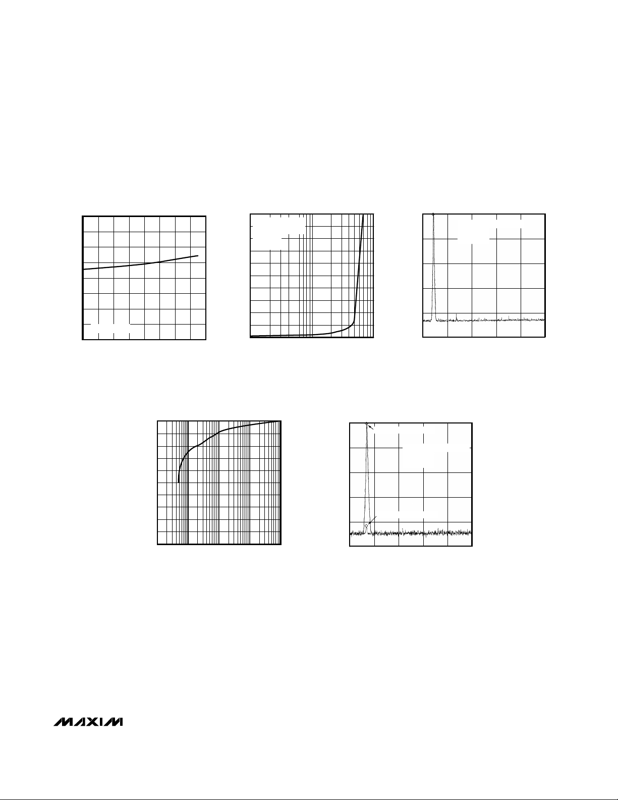
70
1000
950
900
850
800
750
700
650
600
550
500
-55 -40 -20 0 20 40 60 80 100 120
MAX525-03
SUPPLY CURRENT (µA)
SUPPLY CURRENT
vs. TEMPERATURE
TEMPERATURE (°C)
CODE = FFF hex
INL (LSB)
-0.5
0.4 0.8 1.2 1.6 2.0 2.4 2.8 3.2 3.6 4.0
REFERENCE VOLTAGE (V)
MAX525-01
4.4
0.3
0.2
0.1
0
-0.1
-0.2
-0.3
-0.4
RL = 5kΩ
INTEGRAL NONLINEARITY
vs. REFERENCE VOLTAGE
0
-4
-8
-12
-16
-20
0 500k 1M 1.5M 2M 2.5M 3M
MAX525-02
RELATIVE OUTPUT (dB)
REFERENCE VOLTAGE INPUT
FREQUENCY RESPONSE
FREQUENCY (Hz)
REFAB SWEPT 0.67Vp-p
R
L
= 5kΩ
C
L
= 100pF
__________________________________________Typical Operating Characteristics
(V
DD
= +5V, TA = +25°C, unless otherwise noted.)
MAX525
Low-Power, Quad, 12-Bit Voltage-Output DAC
with Serial Interface
4 _______________________________________________________________________________________
ELECTRICAL CHARACTERISTICS (continued)
(VDD= +5V ±10%, AGND = DGND = 0V, REFAB = REFCD = 2.5V, RL= 5kΩ, CL= 100pF, TA= T
MIN
to T
MAX
, unless otherwise
noted. Typical values are at T
A
= +25°C. Output buffer connected in unity-gain configuration (Figure 9).)
CONDITIONS
t
D02
SCLK Fall to DOUT Valid
Propagation Delay
t
D01
SCLK Rise to DOUT Valid
Propagation Delay
ns100t
CP
SCLK Clock Period
ns0t
DH
DIN Hold Time
ns40t
DS
DIN Setup Time
ns0t
CSH
SCLK Rise to CS Rise Hold Time
ns40t
CSS
CS Fall to SCLK Rise Setup Time
ns40t
CH
SCLK Pulse Width High
ns40t
CL
SCLK Pulse Width Low
UNITSMIN TYP MAXSYMBOLPARAMETER
ns100t
CSW
CS Pulse Width High
ns40t
CS1
CS Rise to SCLK Rise Hold Time
ns40t
CS0
SCLK Rise to CS Fall Delay
C
LOAD
= 200pF
C
LOAD
= 200pF
80
80
TIMING CHARACTERISTICS (Figure 6)
ns
ns
MAX525
Low-Power, Quad, 12-Bit Voltage-Output DAC
with Serial Interface
_______________________________________________________________________________________
5
0.50
0
1
100
TOTAL HARMONIC DISTORTION PLUS NOISE
vs. FREQUENCY
0.05
MAX525-05
FREQUENCY (kHz)
THD + NOISE (%)
0.15
0.25
0.35
10
0.45
0.10
0.20
0.30
0.40
DAC CODE = ALL 1s
REFAB = 1Vp-p
R
L
= 5kΩ
C
L
= 100pF
-100
0.5 1.6 3.8
OUTPUT FFT PLOT
-60
0
MAX525-10
FREQUENCY (kHz)
SIGNAL AMPLITUDE (dB)
2.7 4.9 6.0
-20
-40
-80
V
REF
= 1kHz, 0.006V TO 3.6V
R
L
= 5kΩ
C
L
= 100pF
____________________________Typical Operating Characteristics (continued)
(V
DD
= +5V, TA = +25°C, unless otherwise noted.)
4.0 4.2 4.64.4 4.8 5.0 5.2 5.4 5.6
SUPPLY CURRENT
vs. SUPPLY VOLTAGE
MAX525-04
SUPPLY VOLTAGE (V)
SUPPLY CURRENT (µA)
1000
950
900
850
800
750
700
650
600
CODE = FFF hex
0
-5
0.01 0.1 1 10 100
FULL-SCALE ERROR
vs. LOAD
-4
MAX525-09
LOAD (kΩ)
FULL-SCALE ERROR (LSB)
-3
-2
-1
-100
0.5 1.2 2.6
REFERENCE FEEDTHROUGH
AT 1kHz
-60
0
MAX525-11
FREQUENCY (kHz)
SIGNAL AMPLITUDE (dB)
1.9 3.3 4.0
-20
-40
-80
OUTA FEEDTHROUGH
REFAB INPUT SIGNAL
V
REF
= 3.6Vp-p @ 1kHz
R
L
= 5kΩ
C
L
= 100pF
10µs/div
MAJOR-CARRY TRANSITION
MAX525-07
OUTB,
AC COUPLED
100mV/div
CS
5V/div
V
REF
= 2.5V, RL = 5kΩ, CL = 100pF
2µs/div
OUTA,
AC COUPLED
10mV/div
DIGITAL FEEDTHROUGH (SCLK = 100kHz)
MAX525-08
SCLK,
2V/div
CS = PDL = CL = 5V, DIN = 0V
DAC A CODE SET TO 800 hex
V
REF
= 2.5V, RL = 5kΩ, CL = 100pF
DAC A CODE SWITCHING FROM 00B hex TO FFF hex
DAC B CODE SET TO 800 hex
10µs/div
GND
OUTB,
AC COUPLED
10mV/div
ANALOG CROSSTALK
MAX525-12
OUTA,
1V/div
V
REF
= 2.5V, RL = 5kΩ, CL = 100pF
SWITCHING FROM CODE 000 hex TO FB4 hex
OUTPUT AMPLIFIER GAIN = +2
10µs/div
DYNAMIC RESPONSE
MAX525-13
OUTA,
1V/div
V
REF
= 2.5V, RL = 5kΩ, CL = 100pF
MAX525
Low-Power, Quad, 12-Bit Voltage-Output DAC
with Serial Interface
6 _______________________________________________________________________________________
____________________________Typical Operating Characteristics (continued)
(V
DD
= +5V, TA = +25°C, unless otherwise noted.)
MAX525
Low-Power, Quad, 12-Bit Voltage-Output DAC
with Serial Interface
_______________________________________________________________________________________ 7
______________________________________________________________Pin Description
Serial-Data InputDIN9
Serial Clock InputSCLK10
Digital GroundDGND11
Serial-Data OutputDOUT12
User-Programmable Logic OutputUPO13
DAC B Output Amplifier FeedbackFBB5
Reference Voltage Input for DAC A and DAC BREFAB6
Clear All DACs and Registers. Resets all outputs (OUT_, UPO, DOUT) to 0, active low.
CL
7
Chip-Select Input. Active low.
CS
8
DAC B Output VoltageOUTB4
DAC A Output VoltageOUTA3
PIN
DAC A Output Amplifier FeedbackFBA2
Analog GroundAGND1
FUNCTIONNAME
Power-Down Lockout. Active low. Locks out software shutdown if low.
PDL
14
Reference Voltage Input for DAC C and DAC DREFCD15
DAC C Output Amplifier FeedbackFBC16
DAC C Output VoltageOUTC17
DAC D Output VoltageOUTD18
DAC D Output Amplifier FeedbackFBD19
Positive Power SupplyV
DD
20

MAX525
Low-Power, Quad, 12-Bit Voltage-Output DAC
with Serial Interface
8 _______________________________________________________________________________________
_______________Detailed Description
The MAX525 contains four 12-bit, voltage-output digital-to-analog converters (DACs) that are easily
addressed using a simple 3-wire serial interface. It
includes a 16-bit data-in/data-out shift register, and
each DAC has a doubled-buffered input composed of
an input register and a DAC register (see
Functional
Diagram
). In addition to the four voltage outputs, each
amplifier’s negative input is available to the user.
The DACs are inverted R-2R ladder networks that con-
vert 12-bit digital inputs into equivalent analog output
voltages in proportion to the applied reference voltage
inputs. DACs A and B share the REFAB reference input,
while DACs C and D share the REFCD reference input.
The two reference inputs allow different full-scale output
voltage ranges for each pair of DACs. Figure 1 shows a
simplified circuit diagram of one of the four DACs.
Reference Inputs
The two reference inputs accept positive DC and AC
signals. The voltage at each reference input sets the
full-scale output voltage for its two corresponding
DACs. The reference input voltage range is 0V to (V
DD
- 1.4V). The output voltages (V
OUT_)
are represented by
a digitally programmable voltage source as:
V
OUT_
= (V
REF
x NB / 4096) x Gain
where NB is the numeric value of the DAC’s binary
input code (0 to 4095), V
REF
is the reference voltage,
and Gain is the externally set voltage gain.
The impedance at each reference input is code-dependent, ranging from a low value of 10kΩ when both
DACs connected to the reference have an input code
of 555 hex, to a high value exceeding several gigohms
(leakage currents) with an input code of 000 hex.
Because the input impedance at the reference pins is
code-dependent, load regulation of the reference
source is important.
The REFAB and REFCD reference inputs have a 10kΩ
guaranteed minimum input impedance. When the two
reference inputs are driven from the same source, the
effective minimum impedance is 5kΩ. A voltage reference with a load regulation of 6ppm/mA, such as the
MAX873, would typically deviate by 0.025LSB
(0.061LSB worst case) when driving both MAX525 reference inputs simultaneously at 2.5V. Driving the
REFAB and REFCD pins separately improves reference
accuracy.
In shutdown mode, the MAX525’s REFAB and REFCD
inputs enter a high-impedance state with a typical input
leakage current of 0.01µA.
The reference input capacitance is also code dependent and typically ranges from 20pF with an input code
of all 0s to 100pF with an input code of all 1s.
Output Amplifiers
All MAX525 DAC outputs are internally buffered by precision amplifiers with a typical slew rate of 0.6V/µs. Access
to the inverting input of each output amplifier provides
the user greater flexibility in output gain setting/
signal conditioning (see the
Applications Information
sec-
tion).
With a full-scale transition at the MAX525 output, the
typical settling time to ±1/2LSB is 12µs when loaded
with 5kΩ in parallel with 100pF (loads less than 2kΩ
degrade performance).
The MAX525 output amplifier’s output dynamic responses and settling performances are shown in the
Typical
Operating Characteristics
.
Power-Down Mode
The MAX525 features a software-programmable shutdown that reduces supply current to a typical value of
10µA. The power-down lockout (PDL) pin must be high to
enable the shutdown mode. Writing 1100XXXXXXXXXXXX
as the input-control word puts the MAX525 in powerdown mode (Table 1).
OUT_
FB_
SHOWN FOR ALL 1s ON DAC
D0 D9 D10
D11
2R
2R 2R 2R 2R
R R R
REF_
AGND
Figure 1. Simplified DAC Circuit Diagram
In power-down mode, the MAX525 output amplifiers
and the reference inputs enter a high-impedance state.
The serial interface remains active. Data in the input
registers is retained in power-down, allowing the
MAX525 to recall the output states prior to entering
shutdown. Start up from power-down either by recalling
the previous configuration or by updating the DACs
with new data. When powering up the device or bringing it out of shutdown, allow 15µs for the outputs to stabilize.
Serial-Interface Configurations
The MAX525’s 3-wire serial interface is compatible
with both Microwire™ (Figure 2) and SPI™/QSPI™
(Figure 3). The serial input word consists of two address
bits and two control bits followed by 12 data bits
(MSB first), as shown in Figure 4. The 4-bit address/
control code determines the MAX525’s response outlined in Table 1. The connection between DOUT and
the serial-interface port is not necessary, but may be
used for data echo. Data held in the MAX525’s shift
register can be shifted out of DOUT and returned to the
microprocessor (µP) for data verification.
The MAX525’s digital inputs are double buffered.
Depending on the command issued through the serial
interface, the input register(s) can be loaded without
affecting the DAC register(s), the DAC register(s) can
be loaded directly, or all four DAC registers can be
updated simultaneously from the input registers
(Table 1).
Serial-Interface Description
The MAX525 requires 16 bits of serial data. Table 1 lists
the serial-interface programming commands. For certain commands, the 12 data bits are “don’t cares.” Data
is sent MSB first and can be sent in two 8-bit packets or
one 16-bit word (CS must remain low until 16 bits are
transferred). The serial data is composed of two DAC
address bits (A1, A0) and two control bits (C1, C0),
followed by the 12 data bits D11…D0 (Figure 4). The
4-bit address/control code determines:
• The register(s) to be updated
• The clock edge on which data is to be clocked out
via the serial-data output (DOUT)
• The state of the user-programmable logic output
(UPO)
• If the part is to go into shutdown mode (assuming
PDL is high)
• How the part is configured when coming out of shutdown mode.
MAX525
Low-Power, Quad, 12-Bit Voltage-Output DAC
with Serial Interface
_______________________________________________________________________________________ 9
SCLK
DIN
DOUT*
CS
SK
SO
SI*
I/O
MAX525
MICROWIRE
PORT
*THE DOUT-SI CONNECTION IS NOT REQUIRED FOR WRITING TO THE MAX525,
BUT MAY BE USED FOR READBACK PURPOSES.
Figure 2. Connections for Microwire
DOUT*
DIN
SCLK
CS
MISO*
MOSI
SCK
I/O
SPI/QSPI
PORT
SS
+5V
CPOL = 0, CPHA = 0
*THE DOUT-MISO CONNECTION IS NOT REQUIRED FOR WRITING TO THE MAX525,
BUT MAY BE USED FOR READBACK PURPOSES.
MAX525
Figure 3. Connections for SPI/QSPI
Figure 4. Serial-Data Format
MSB..................................................................................LSB
16 Bits of Serial Data
Address
Bits
Control
Bits
Data Bits
MSB.............................................LSB
A1 A0 C1 C0 D11................................................D0
12 Data Bits
4 Address/
Control Bits

C1 C0
MAX525
Figure 5 shows the serial-interface timing requirements.
The chip-select pin (CS) must be low to enable the
DAC’s serial interface. When CS is high, the interface
control circuitry is disabled. CS must go low at least
t
CSS
before the rising serial clock (SCLK) edge to properly clock in the first bit. When CS is low, data is
clocked into the internal shift register via the serial-data
input pin (DIN) on SCLK’s rising edge. The maximum
guaranteed clock frequency is 10MHz. Data is latched
into the appropriate MAX525 input/DAC registers on
CS’s rising edge.
The programming command Load-All-DACs-From-ShiftRegister allows all input and DAC registers to be simultaneously loaded with the same digital code from the
input shift register. The no operation (NOP) command
leaves the register contents unaffected and is useful
when the MAX525 is configured in a daisy chain (see
the
Daisy Chaining Devices
section). The command to
change the clock edge on which serial data is shifted
out of DOUT also loads data from all input registers to
their respective DAC registers.
Serial-Data Output (DOUT)
The serial-data output, DOUT, is the internal shift register’s output. The MAX525 can be programmed so that
data is clocked out of DOUT on SCLK’s rising edge
(Mode 1) or falling edge (Mode 0). In Mode 0, output
data at DOUT lags input data at DIN by 16.5 clock
cycles, maintaining compatibility with Microwire™,
SPI™/QSPI™, and other serial interfaces. In Mode 1,
output data lags input data by 16 clock cycles. On
power-up, DOUT defaults to Mode 0 timing.
User-Programmable Logic Output (UPO)
The user-programmable logic output, UPO, allows an
external device to be controlled via the MAX525 serial
interface (Table 1).
Low-Power, Quad, 12-Bit Voltage-Output DAC
with Serial Interface
10 ______________________________________________________________________________________
Table 1. Serial-Interface Programming Commands
0 0 No operation (NOP) to DAC registers
0 0
1 1
UPO goes low (default)
Shutdown (provided PDL = 1)
1 0 Load all DAC registers from shift register (start-up).
Load input register A; DAC registers unchanged.
Load input register B; DAC registers unchanged.
Load input register C; DAC registers unchanged.
Load input register D; DAC registers unchanged.
Load input register A; all DAC registers updated.
Load input register B; all DAC registers updated.
Load input register C; all DAC registers updated.
Load input register D; all DAC registers updated.
0 1
0 1
0 0
0 1
1 0
1 1
0 0
0 1
1 0
1 1
Update all DAC registers from their respective input registers (start-up).
UPO goes high
0 0
1 0
0 0
0 0
0 0
1 0
0 1
0 1
0 1
0 1
1 1
1 1
1 1
1 1
XXXXXXXXXXXX
16-BIT SERIAL WORD
XXXXXXXXXXXX
XXXXXXXXXXXX
12-bit DAC data
XXXXXXXXXXXX
XXXXXXXXXXXX
12-bit DAC data
12-bit DAC data
12-bit DAC data
12-bit DAC data
12-bit DAC data
12-bit DAC data
12-bit DAC data
12-bit DAC data
1 0
XXXXXXXXXXXX
Mode 0, DOUT clocked out on SCLK’s falling edge. All DAC registers
updated (default).
XXXXXXXXXXXX
1 1
Mode 1, DOUT clocked out on SCLK’s rising edge. All DAC registers
updated.
1 0
1 0
“X” = Don’t care
A1 A0 C1 C0
D11.................D0
MSB LSB
FUNCTION

Power-Down Lockout (
PDL
)
The power-down lockout pin PDL disables software
shutdown when low. When in shutdown, transitioning
PDL from high to low wakes up the part with the output
set to the state prior to shutdown. PDL could also be
used to asynchronously wake up the device.
Daisy Chaining Devices
Any number of MAX525s can be daisy chained by connecting the DOUT pin of one device to the DIN pin of
the following device in the chain (Figure 7).
Since the MAX525’s DOUT pin has an internal active
pull-up, the DOUT sink/source capability determines
the time required to discharge/charge a capacitive
load. Refer to the serial-data-out V
OH
and VOLspecifi-
cations in the
Electrical Characteristics.
Figure 8 shows an alternate method of connecting several MAX525s. In this configuration, the data bus is
common to all devices; data is not shifted through a
daisy chain. More I/O lines are required in this configuration because a dedicated chip-select input (CS) is
required for each IC.
MAX525
Low-Power, Quad, 12-Bit Voltage-Output DAC
with Serial Interface
______________________________________________________________________________________ 11
CS
SCLK
DIN
DOUT
(MODE 1)
MSB FROM
PREVIOUS WRITE
MSB FROM
PREVIOUS WRITE
COMMAND
EXECUTED
9
8
16
1
A0
A1 D0
C1
C0
D11
D10
D9
D6
D5
D4
D3
D2
D1
D8
D7
DOUT
(MODE 0)
A0
A1 D0 A1
C1
C0
D11
D10
D9
D6
D5
D4
D3
D2
D1
D8
D7
A0
A1 D0 A1
C1
C0
D11
D10
D9
D6
D5
D4
D3
D2
D1
D8
D7
DATA PACKET (N)
DATA PACKET (N-1)
DATA PACKET (N)
DATA PACKET (N-1)
DATA PACKET (N)
Figure 5. Serial-Interface Timing Diagram
SCLK
DIN
DOUT
t
CSO
t
CSS
t
CL
t
CH
t
CP
t
DO1
t
CSW
t
CS1
t
DO2
t
CSH
t
DS
t
DH
CS
Figure 6. Detailed Serial-Interface Timing Diagram

MAX525
Low-Power, Quad, 12-Bit Voltage-Output DAC
with Serial Interface
12 ______________________________________________________________________________________
DIN
CS
TO OTHER
SERIAL DEVICES
MAX525
SCLK
DIN
CS
DOUT
MAX525
SCLK
DIN
CS
DOUT
MAX525
SCLK
DIN
CS
DOUT
SCLK
Figure 7. Daisy-Chaining MAX525s
TO OTHER
SERIAL DEVICES
MAX525
DIN
SCLK
CS
MAX525
DIN
SCLK
CS
MAX525
DIN
SCLK
CS
DIN
SCLK
CS1
CS2
CS3
Figure 8. Multiple MAX525s Sharing a Common DIN Line

__________Applications Information
Unipolar Output
For a unipolar output, the output voltages and the reference inputs have the same polarity. Figure 9 shows the
MAX525 unipolar output circuit, which is also the typical operating circuit. Table 2 lists the unipolar output
codes.
For rail-to-rail outputs, see Figure 10. This circuit shows
the MAX525 with the output amplifiers configured with a
closed-loop gain of +2 to provide 0V to 5V full-scale
range when a 2.5V reference is used.
Bipolar Output
The MAX525 outputs can be configured for bipolar
operation using Figure 11’s circuit.
V
OUT
= V
REF
[(2NB / 4096) - 1]
where NB is the numeric value of the DAC’s binary
input code. Table 3 shows digital codes (offset binary)
and corresponding output voltages for Figure 11’s
circuit.
MAX525
Low-Power, Quad, 12-Bit Voltage-Output DAC
with Serial Interface
______________________________________________________________________________________ 13
Table 2. Unipolar Code Table
Table 3. Bipolar Code Table
Note: 1LSB = (V
REF
) (
4096
)
1
DAC CONTENTS
ANALOG OUTPUT
MSB LSB
4095
1111 1111 1111 +V
REF
(——— )
4096
2049
1000 0000 0001 +V
REF
(——— )
4096
2048 +V
REF
1000 0000 0000 +V
REF
(——— )= ————
4096 2
2047
0111 1111 1111 +V
REF
(——— )
4096
1
0000 0000 0001 +V
REF
(——— )
4096
0000 0000 0000 0V
DAC CONTENTS
ANALOG OUTPUT
MSB LSB
2047
1111 1111 1111 +V
REF
(——— )
2048
1
1000 0000 0001 +V
REF
(——— )
2048
1000 0000 0000 0V
1
0111 1111 1111 -V
REF
(——— )
2048
2047
0000 0000 0001 -V
REF
(——— )
2048
2048
0000 0000 0000 -V
REF
(——— )= -V
REF
2048
Figure 9. Unipolar Output Circuit
MAX525
REFAB
REFERENCE INPUTS
REFCD
DAC A
DAC B
DAC C
DAC D
+5V
V
DD
DGNDAGND
FBA
OUTA
FBB
OUTB
FBC
OUTC
FBD
OUTD

MAX525
Using an AC Reference
In applications where the reference has AC signal components, the MAX525 has multiplying capability within
the reference input range specifications. Figure 12
shows a technique for applying a sine-wave signal to
the reference input where the AC signal is offset before
being applied to REFAB/REFCD. The reference voltage
must never be more negative than DGND.
The MAX525’s total harmonic distortion plus noise (THD
+ N) is typically less than -72dB, given a 1Vp-p signal
swing and input frequencies up to 25kHz. The typical
-3dB frequency is 650kHz, as shown in the
Typical
Operating Characteristics
graphs.
Digitally Programmable Current Source
The circuit of Figure 13 places an NPN transistor
(2N3904 or similar) within the op-amp feedback loop to
implement a digitally programmable, unidirectional current source. This circuit can be used to drive 4mA to
20mA current loops, which are commonly used in
industrial-control applications. The output current is calculated with the following equation:
I
OUT
= (V
REF
/ R) x (NB / 4096)
where NB is the numeric value of the DAC’s binary
input code and R is the sense resistor shown in
Figure 13.
Low-Power, Quad, 12-Bit Voltage-Output DAC
with Serial Interface
14 ______________________________________________________________________________________
MAX525
DAC A
DAC B
DAC C
DAC D
V
REFAB
= V
REFCD
= 2.5V
OUTA
10k
10k
10k
10k
10k
10k
10k
10k
OUTB
OUTC
OUTD
DGNDAGND
REFAB
REFCD
REFERENCE INPUTS
+5V
V
DD
FBA
FBB
FBC
FBD
Figure 10. Unipolar Rail-to-Rail Output Circuit
DAC
V
OUT
+5V
-5V
R1 = R2 = 10kΩ ± 0.1%
MAX525
REF_
R1
R2
FB_
OUT_
Figure 11. Bipolar Output Circuit
DAC_
OUT_
MAX525
10k
26k
REF_
V
DD
AGND DGND
+5V
AC
REFERENCE
INPUT
500mVp-p
1/2 MAX492
Figure 12. AC Reference Input Circuit

Power-Supply Considerations
On power-up, all input and DAC registers are cleared
(set to zero code) and DOUT is in Mode 0 (serial data
is shifted out of DOUT on the clock’s falling edge).
For rated MAX525 performance, limit REFAB/REFCD to
less than 1.4V below VDD. Bypass VDDwith a 4.7µF
capacitor in parallel with a 0.1µF capacitor to AGND.
Use short lead lengths and place the bypass capacitors as close to the supply pins as possible.
Grounding and Layout Considerations
Digital or AC transient signals between AGND and
DGND can create noise at the analog outputs. Tie
AGND and DGND together at the DAC, then tie this
point to the highest-quality ground available.
Good printed circuit board ground layout minimizes
crosstalk between DAC outputs, reference inputs, and
digital inputs. Reduce crosstalk by keeping analog
lines away from digital lines. Wire-wrapped boards are
not recommended.
MAX525
Low-Power, Quad, 12-Bit Voltage-Output DAC
with Serial Interface
______________________________________________________________________________________ 15
DAC_
MAX525
REF_
OUT_
R
I
OUT
2N3904
V
L
FB_
Figure 13. Digitally Programmable Current Source
__________________Pin Configuration
20
19
18
17
16
15
14
13
1
2
3
4
5
6
7
8
V
DD
FBD
OUTD
OUTCOUTB
OUTA
FBA
AGND
TOP VIEW
FBC
REFCD
PDL
UPOCS
CL
REFAB
FBB
12
11
9
10
DOUT
DGNDSCLK
DIN
DIP/SSOP
MAX525
MAX525
Low-Power, Quad, 12-Bit Voltage-Output DAC
with Serial Interface
.
_Ordering Information (continued) ___________________Chip Information
________________________________________________________Package Information
PART
MAX525BC/D
MAX525AEPP -40°C to +85°C
0°C to +70°C
TEMP. RANGE PIN-PACKAGE
Dice*
20 Plastic DIP
INL
(LSBs)
±1
±1/2
* Dice are specified at TA= +25°C, DC parameters only.
**Contact factory for availability and processing to MIL-STD-883.
MAX525BEPP
MAX525AEAP
MAX525BEAP -40°C to +85°C
-40°C to +85°C
-40°C to +85°C 20 Plastic DIP
20 SSOP
20 SSOP
±1
±1/2
±1
MAX525AMJP
MAX525BMJP -55°C to +125°C
-55°C to +125°C 20 CERDIP**
20 CERDIP**
±1/2
±1
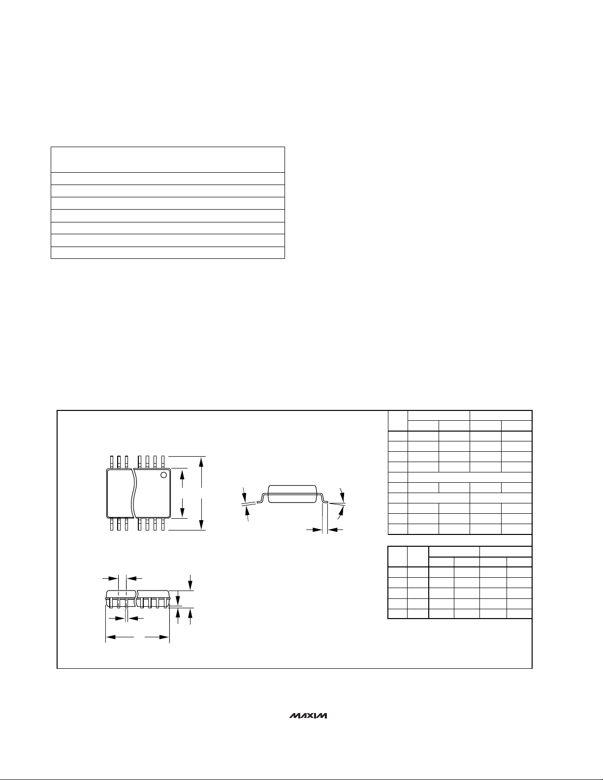
L
DIM
A
A1
B
C
D
E
e
H
L
α
DIM
D
D
D
D
D
MIN
0.068
0.002
0.010
0.004
0.205
0.301
0.025
0˚
MIN
0.239
0.239
0.278
0.317
0.397
MAX
0.078
0.008
0.015
0.008
0.209
0.311
0.037
8˚
MAX
0.249
0.249
0.289
0.328
0.407
MIN
1.73
0.05
0.25
0.09
5.20
7.65
0.63
0˚
MIN
6.07
6.07
7.07
8.07
10.07
MAX
1.99
0.21
0.38
0.20
5.38
7.90
0.95
8˚
PINS
14
16
20
24
28
MAX
6.33
6.33
7.33
8.33
10.33
INCHES
INCHES
MILLIMETERS
MILLIMETERS
α
SSOP
SHRINK
SMALL-OUTLINE
PACKAGE
HE
D
A
A1
C
B
0.65 BSC0.0256 BSC
21-0056A
e
SEE VARIATIONS
TRANSISTOR COUNT: 4337
Maxim cannot assume responsibility for use of any circuitry other than circuitry entirely embodied in a Maxim product. No circuit patent licenses are
implied. Maxim reserves the right to change the circuitry and specifications without notice at any time.
16
____________________Maxim Integrated Products, 120 San Gabriel Drive, Sunnyvale, CA 94086 408-737-7600
© 1997 Maxim Integrated Products Printed USA is a registered trademark of Maxim Integrated Products.
 Loading...