

Page 1
General Description
The MAX5182 is a dual, 10-bit, alternate-phase-update,
current-output digital-to-analog converter (DAC)
designed for superior performance in systems requiring
analog signal reconstruction with low distortion and
low-power operation. The MAX5185 provides equal
specifications with on-chip output resistors for voltageoutput operation. Both devices are designed for 10pV-s
glitch operation, to reduce distortion and minimize
unwanted spurious signal components at the output. An
on-board +1.2V bandgap circuit provides a well-regulated, low-noise reference that can be disabled for
external reference operation.
The MAX5182/MAX5185 are designed to provide a high
level of signal integrity for the least amount of power dissipation. Both DACs operate from a +2.7V to +3.3V single supply. Additionally, these DACs have three modes
of operation: normal, low-power standby, and complete
shutdown. A full shutdown provides the lowest possible
power dissipation with a maximum shutdown current of
1µA. Fast wake-up time (0.5µs) from standby mode to
full DAC operation allows for power conservation by
activating the DACs only when required.
The MAX5182/MAX5185 are available in a 28-pin QSOP
package and are specified for the extended (-40°C to
+85°C) temperature range. For pin-compatible 8-bit
versions, refer to the MAX5188/MAX5191 data sheet.
Applications
Signal Reconstruction
Digital Signal Processing
Arbitrary Waveform Generators (AWGs)
Imaging Applications
Features
♦ +2.7V to +3.3V Single-Supply Operation
♦ Wide Spurious-Free Dynamic Range: 70dB at
f
OUT
= 2.2MHz
♦ Fully-Differential Outputs for Each DAC
♦ ±0.5% FSR Gain Mismatch Between DAC Outputs
♦ Low-Current Standby or Full-Shutdown Modes
♦ Internal +1.2V Low-Noise Bandgap Reference
♦ Small 28-Pin QSOP Package
MAX5182/MAX5185
Dual, 10-Bit, 40MHz Current/Voltage
Alternate-Phase Output DACs
________________________________________________________________ Maxim Integrated Products 1
19-1578; Rev 3; 12/01
PART
MAX5182BEEI
-40°C to +85°C
TEMP. RANGE PIN-PACKAGE
28 QSOP
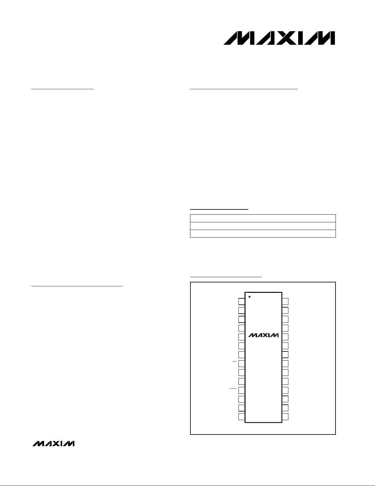
Pin Configuration
Ordering Information
MAX5185BEEI
-40°C to +85°C 28 QSOP
For pricing, delivery, and ordering information, please contact Maxim/Dallas Direct! at
1-888-629-4642, or visit Maxim’s website at www.maxim-ic.com.
TOP VIEW
CREF1
OUT1P
OUT1N
AGND
AV
DACEN
CLK
N.C.
REN
1
2
3
4
5
DD
PD
CS
D0
D1
D2
MAX5182
6
MAX5185
7
8
9
10
11
12
13
14
QSOP
28
CREF2
27
OUT2P
26
OUT2N
25
REFO
24
REFR
23
DGND
22
DV
DD
21
D9
20
D8
19
D7
18
D6
17
D5
16
D4
15
D3
Page 2
LSB
2 _______________________________________________________________________________________
ABSOLUTE MAXIMUM RATINGS
ELECTRICAL CHARACTERISTICS
(AVDD= DVDD= +3V ±10%, AGND = DGND = 0, f
CLK
= 40MHz, IFS= 1mA, 400Ω differential output, CL= 5pF, TA= T
MIN
to T
MAX
,
unless otherwise noted. Typical values are at T
A
= +25°C.)
Stresses beyond those listed under “Absolute Maximum Ratings” may cause permanent damage to the device. These are stress ratings only, and functional
operation of the device at these or any other conditions beyond those indicated in the operational sections of the specifications is not implied. Exposure to
absolute maximum rating conditions for extended periods may affect device reliability.
AVDD, DVDDto AGND, DGND .................................-0.3V to +6V
Digital Inputs to DGND.............................................-0.3V to +6V
OUT1P, OUT1N, OUT2P, OUT2N, CREF1,
CREF2 to AGND ...................................................-0.3V to +6V
V
REF
to AGND ..........................................................-0.3V to +6V
AGND to DGND.....................................................-0.3V to +0.3V
AVDDto DVDD.................................................................... ±3.3V
Maximum Current into Any Pin............................................50mA
Continuous Power Dissipation (T
A
= +70°C)
28-Pin QSOP (derate 9.00mW/°C above +70°C)....... 725mW
Operating Temperature Ranges
MAX518_BEEI................................................-40°C to +85°C
Storage Temperature Range .............................-65°C to +150°C
Lead Temperature (soldering, 10s) ................................ +300°C
MAX5182/MAX5185
dB
f
CLK
= 40MHz
Full-Scale Output Current I
FS
0.5 1 1.5
mA
DAC External Output Resistor
Load
R
L
400
Ω
MAX5182 only
MAX5182 only
PARAMETER SYMBOL MIN TYP MAX UNITS
Full-Scale Error
-40 ±15 +40
LSB
-2 +2
Differential Nonlinearity DNL
-1 ±0.5 +1
LSB
Output Settling Time
25
ns
Glitch Impulse
10
pVs
Spurious-Free Dynamic Range
to Nyquist
SFDR
72
dBc
57 70
Resolution N
10
Bits
Integral Nonlinearity INL
-2 ±0.5 +2
LSB
Total Harmonic Distortion to
Nyquist
THD
-70
dB
-68 -63
Signal-to-Noise Ratio to
Nyquist
SNR
61
dB
56 59
DAC-to-DAC Ouput Isolation
-60
dB
Clock and Data Feedthrough
50
nVs
Output Noise
10
pA/√Hz
Gain Mismatch Between
DAC Outputs
±0.5 ±1
% FSR
Full-Scale Output Voltage V
FS
400
mV
Voltage Compliance of Output
-0.3 0.8
V
Output Leakage Current
-1 1
µA
CONDITIONS
f
CLK
= 40MHz
(Note 1)
MAX5182
Guaranteed monotonic
To ±0.5LSB error band
f
CLK
= 40MHz
f
OUT
= 2.2MHz
All 0s to all 1s
f
OUT
= 2.2MHz, TA= +25°C
DACEN = 0, MAX5182 only
-8 +8
MAX5185
Zero-Scale Error
STATIC PERFORMANCE
DYNAMIC PERFORMANCE
ANALOG OUTPUT
Dual, 10-Bit, 40MHz Current/Voltage
Alternate-Phase Output DACs
f
OUT
= 550kHz
f
OUT
= 2.2MHz, TA= +25°C
f
OUT
= 550kHz
f
OUT
= 2.2MHz, TA= +25°C
f
OUT
= 550kHz
f
OUT
= 2.2MHz, TA= +25°C
Page 3
MAX5182/MAX5185
Dual, 10-Bit, 40MHz Current/Voltage
Alternate-Phase Output DACs
_______________________________________________________________________________________ 3
ELECTRICAL CHARACTERISTICS (continued)
(AVDD= DVDD= +3V ±10%, AGND = DGND = 0, f
CLK
= 40MHz, IFS= 1mA, 400Ω differential output, CL= 5pF, TA= T
MIN
to T
MAX
,
unless otherwise noted. Typical values are at T
A
= +25°C.)
Note 1: Excludes reference and reference resistor (MAX5185) tolerance.
CS Fall to CLK Rise Time
5
ns
CS Fall to CLK Fall Time
5
ns
DACEN Rise Time to V
OUT_
0.5
µs
PD Fall Time to V
OUT_
50
µs
Clock Period t
CLK
25
ns
Clock High Time t
CH
10 0
ns
Clock Low Time t
CL
10
ns
Digital Input Voltage High V
IH
2
V
Digital Input Voltage Low V
IL
0.8
V
Digital Input Current I
IN
±1
µA
Digital Input Capacitance C
IN
10
pF
DAC1 DATA to CLK Rise
Setup Time
t
DS1
10
ns
DAC2 DATA to CLK Fall
Setup Time
t
DS2
10
ns
DAC1 CLK Rise to DATA
Hold Time
t
DH1
0
ns
DAC2 CLK Fall to DATA
Hold Time
t
DH2
0
ns
VIN= 0 or DV
DD
Output Voltage Temperature Drift TCV
REF
50
ppm/°C
Reference Output Drive
Capability
I
REFOUT
10
µA
Reference Supply Rejection
0.5
mV/V
Current Gain (IFS/ I
REF
)
8
mA/mA
Analog Power-Supply Voltage AV
DD
2.7 3.3
V
Analog Supply Current I
AVDD
2.7 5.0
mA
Digital Power-Supply Voltage DV
DD
2.7 3.3
V
Digital Supply Current I
DVDD
4.2 5.0
mA
Standby Current I
STANDBY
1.0 1.5
mA
Shutdown Current I
SHDN
0.5 1
µA
PD = 0, DACEN = 1, digital inputs at 0
or DV
DD
PD = 0, DACEN = 1, digital inputs at 0
or DV
DD
PD = 0, DACEN = 0, digital inputs at 0
or DV
DD
PD = 1, DACEN = X, digital inputs at 0
or DV
DD
(X = don’t care)
PARAMETER SYMBOL MIN TYP MAX UNITSCONDITIONS
Output Voltage Range V
REF
2.7 1.2 1.28 V
REFERENCE
POWER REQUIREMENTS
LOGIC INPUTS AND OUTPUTS
TIMING CHARACTERISTICS
Page 4
MAX5182/MAX5185
Dual, 10-Bit, 40MHz Current/Voltage
Alternate-Phase Output DACs
4 _______________________________________________________________________________________
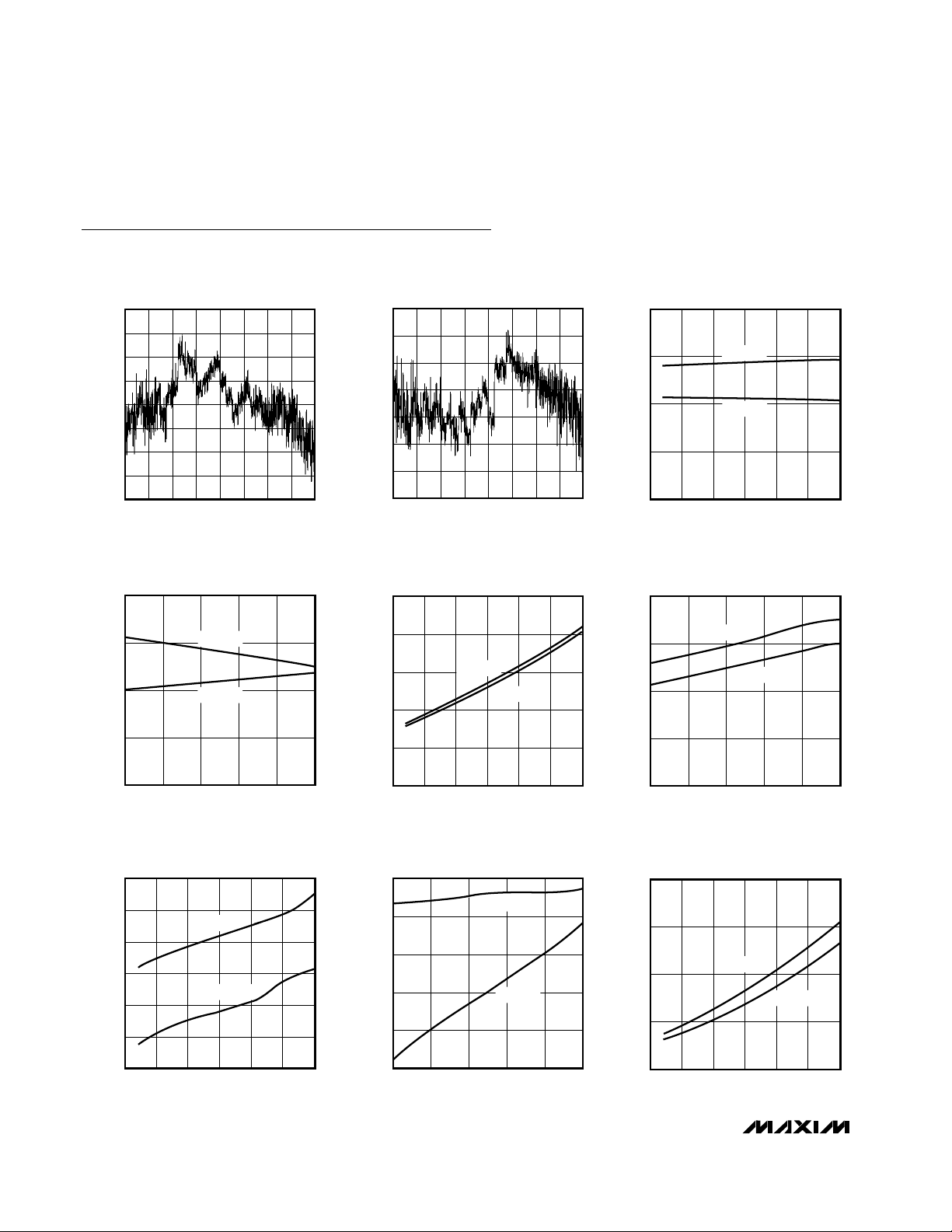
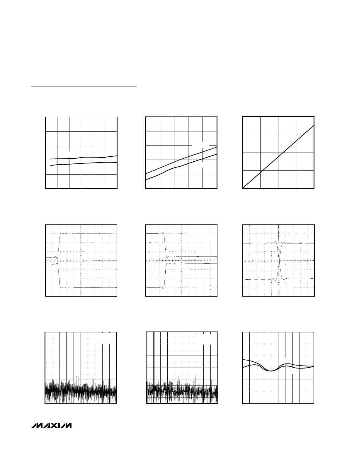
Typical Operating Characteristics
(AVDD= DVDD= +3V, AGND = DGND = 0, 400Ω differential output, IFS= 1mA, CL= 5pF, TA= +25°C, unless otherwise noted.)
0.6
0.5
0.4
0.3
0.2
0.1
0
-0.1
-0.2
0 128 256 384 512 640 768 896 1024
INTEGRAL NONLINEARITY
vs. INPUT CODE
MAX5182/85-01
INPUT CODE
INL (LSB)
0.4
0.3
0.2
0.1
0
-0.1
-0.2
-0.3
0 128 256 384 512 640 768 896 1024
DIFFERENTIAL NONLINEARITY
vs. INPUT CODE
MAX5182/85-02
INPUT CODE
DNL (LSB)
3.00
2.75
2.50
2.25
2.00
2.5 4.03.0 3.5 4.5 5.0 5.5
ANALOG SUPPLY CURRENT
vs. SUPPLY VOLTAGE
MAX5182/85-03
SUPPLY VOLTAGE (V)
ANALOG SUPPLY CURRENT (mA)
MAX5182
MAX5185
3.00
2.75
2.25
2.50
2.00
-40 35-15 10 60 85
ANALOG SUPPLY CURRENT
vs. TEMPERATURE
MAX5182/85-04
TEMPERATURE (°C)
ANALOG SUPPLY CURRENT (mA)
MAX5182
MAX5185
10
8
6
4
2
0
2.5 4.03.0 3.5 4.5 5.0 5.5
DIGITAL SUPPLY CURRENT
vs. SUPPLY VOLTAGE
MAX5182/85-05
SUPPLY VOLTAGE (V)
DIGITAL SUPPLY CURRENT (mA)
MAX5182
MAX5185
4.00
3.75
3.25
3.50
3.00
-40 35-15 10 60 85
DIGITAL SUPPLY CURRENT
vs. TEMPERATURE
MAX5182/85-06
TEMPERATURE (°C)
DIGITAL SUPPLY CURRENT (mA)
MAX5182
MAX5185
620
610
600
580
590
570
560
2.5 4.03.0 3.5 4.5 5.0 5.5
STANDBY CURRENT
vs. SUPPLY VOLTAGE
MAX5182/85-07
SUPPLY VOLTAGE (V)
STANDBY CURRENT (µA)
MAX5182
MAX5185
600
590
570
560
580
550
-40 35-15 10 60 85
MAX5182/MAX5185
STANDBY CURRENT vs. TEMPERATURE
MAX5182/85-08
TEMPERATURE (°C)
STANDBY CURRENT (mA)
MAX5182
MAX5185
0.8
0.7
0.6
0.5
0.4
2.5 4.03.0 3.5 4.5 5.0 5.5
SHUTDOWN CURRENT
vs. SUPPLY VOLTAGE
MAX5182/85-09
SUPPLY VOLTAGE (V)
SHUTDOWN CURRENT (µA)
MAX5182
MAX5185
Page 5
MAX5182/MAX5185
Dual, 10-Bit, 40MHz Current/Voltage
Alternate-Phase Output DACs
_______________________________________________________________________________________ 5
)
Typical Operating Characteristics (continued)
(AVDD= DVDD= +3V, AGND = DGND = 0, 400Ω differential output, IFS= 1mA, CL= 5pF, TA= +25°C, unless otherwise noted.)
INTERNAL REFERENCE VOLTAGE
vs. SUPPLY VOLTAGE
1.28
INTERNAL REFERENCE VOLTAGE
vs. TEMPERATURE
1.28
4
OUTPUT CURRENT
vs. REFERENCE CURRENT
1.27
1.26
MAX5182
1.25
REFERENCE VOLTAGE (V)
1.24
1.23
2.5 4.03.0 3.5 4.5 5.0 5.5
MAX5185
SUPPLY VOLTAGE (V)
DYNAMIC RESPONSE RISE TIME
MAX5182/85-11
1.27
1.26
1.25
REFERENCE VOLTAGE (V)
1.24
1.23
MAX5182/85-14
OUT_P
150mV/
div
OUT_N
150mV/
div
MAX5182
MAX5185
-40 35-15 10 60 85
TEMPERATURE (°C)
DYNAMIC RESPONSE FALL TIME
MAX5182/85-12
3
2
OUTPUT CURRENT (mA)
1
0
MAX5182/85-15
OUT_P
150mV/
div
OUT_N
150mV/
div
0 125 250 375 500
REFERENCE CURRENT (µA)
SETTLING TIME
MAX5182/85-13
MAX5182/85-16
OUT_N
100mV/
div
OUT_P
100mV/
div
0
-10
-20
-30
-40
-50
-60
(dBc)
-70
-80
-90
-100
-110
-120
0246
50ns/div
50ns/div
12.5ns/div
SPURIOUS-FREE DYNAMIC RANGE
FFT PLOT, DAC1
f
OUT
f
CLK
81012141618
OUTPUT FREQUENCY (MHz)
= 2.2MHz
= 40MHz
20
MAX5181/4toc17
0
-10
-20
-30
-40
-50
-60
(dBc)
-70
-80
-90
-100
-110
-120
0246
FFT PLOT, DAC2
f
OUT
f
CLK
81012141618
OUTPUT FREQUENCY (MHz)
= 2.2MHz
= 40MHz
20
MAX5182/85-18
100
vs. CLOCK FREQUENCY
90
80
70
SFDR (dBc)
60
50
40
10 302515 20 35 40 45 50 55 60
CLOCK FREQUENCY (MHz
DAC2
MAX5182/85-19
DAC1
Page 6

MAX5182/MAX5185
Dual, 10-Bit, 40MHz Current/Voltage
Alternate-Phase Output DACs
6 _______________________________________________________________________________________
Typical Operating Characteristics (continued)
(AVDD= DVDD= +3V, AGND = DGND = 0, 400Ω differential output, IFS= 1mA, CL= 5pF, TA= +25°C, unless otherwise noted.)
SPURIOUS-FREE DYNAMIC RANGE vs. OUTPUT
FREQUENCY AND CLOCK FREQUENCY, DAC1
78
f
= 40MHz
76
f
= 20MHz
CLK
74
72
SFDR (dBc)
70
68
66
f
CLK
500 1100 1300700 900 1500 1700 1900 2100 2300
OUTPUT FREQUENCY (kHz)
f
CLK
= 50MHz
f
CLK
CLK
= 60MHz
= 10MHz
f
= 30MHz
CLK
MAX5182/85-20
SPURIOUS-FREE DYNAMIC RANGE vs. OUTPUT
FREQUENCY AND CLOCK FREQUENCY, DAC2
78
f
= 50MHz f
CLK
76
74
72
SFDR (dBc)
70
68
66
f
CLK
500 1100 1300700 900 1500 1700 1900 2100 2300
= 20MHz
CLK
= 10MHz
f
= 60MHz
CLK
f
CLK
OUTPUT FREQUENCY (kHz)
= 30MHz
CLK
= 40MHzf
MAX5182/85-21
SIGNAL-TO-NOISE PLUS DISTORTION
vs. OUTPUT FREQUENCY
62.5
62.0
61.5
SINAD (dB)
61.0
60.5
60.0
0 1500500 1000 2000 2500
OUTPUT FREQUENCY (kHz)
DAC1
MULTITONE SPURIOUS-FREE DYNAMIC RANGE
vs. OUTPUT FREQUENCY
20
0
-20
-40
-60
SFDR (dBc)
-80
-100
-120
-140
06421081412 1816 20
OUTPUT FREQUENCY (MHz)
MAX5182/85-25
SPURIOUS-FREE DYNAMIC RANGE
vs. FULL-SCALE OUTPUT CURRENT
74
72
70
68
SFDR (dBc)
66
64
62
60
0.50 0.75 1.00 1.25 1.50
FULL-SCALE OUTPUT CURRENT (mA)
MAX5182/85-26
MAX5182/85-23
DAC2
Page 7

MAX5182/MAX5185
Dual, 10-Bit, 40MHz Current/Voltage
Alternate-Phase Output DACs
_______________________________________________________________________________________ 7
Clock InputCLK9
No Connection. Do not connect to this pin.
N.C.10
Active-Low Reference Enable. Connect to DGND to activate the on-chip +1.2V reference.
REN
11
Data Bit D0 (LSB) to Data Bit D9 (MSB)D0–D912–21
Digital Supply, +2.7V to +3.3VDV
DD
22
Analog Positive Supply, +2.7V to +3.3VAV
DD
5
DAC Enable, Digital Input
0: Enter DAC standby mode with PD = DGND
1: Power-up DAC with PD = DGND
X: Enter shutdown mode with PD = DV
DD
(X = don’t care)
DACEN6
Power-Down Select
0: Enter DAC standby mode (DACEN = DGND) or power-up DAC (DACEN = DV
DD
)
1: Enter shutdown mode
PD7
Active-Low Chip Select
CS
8
Analog GroundAGND4
Negative Analog Output, DAC1. Current output for MAX5182; voltage output for MAX5185.OUT1N3
PIN
Positive Analog Output, DAC1. Current output for MAX5182; voltage output for MAX5185.OUT1P2
Reference Bias Bypass, DAC1CREF11
FUNCTIONNAME
Positive Analog Output, DAC2. Current output for MAX5182; voltage output for MAX5185.OUT2P27
Reference Bias Bypass, DAC2CREF228
Negative Analog Output, DAC2. Current output for MAX5182; voltage output for MAX5185.OUT2N26
Reference OutputREFO25
Reference InputREFR24
Digital GroundDGND23
______________________________________________________________Pin Description
Page 8

MAX5182/MAX5185
Dual, 10-Bit, 40MHz Current/Voltage
Alternate-Phase Output DACs
8 _______________________________________________________________________________________
Detailed Description
The MAX5182/MAX5185 are dual, 10-bit digital-to-analog converters (DACs) capable of operating with clock
speeds up to 40MHz. Each of these dual converters
consists of separate input and DAC registers, followed
by a current-source array capable of generating up to
1.5mA full-scale output current (Figure 1). An integrated
+1.2V voltage reference and control amplifier determine
the data converters’ full-scale output currents/voltages.
Careful reference design ensures close gain matching
and excellent drift characteristics. The MAX5185, with
its voltage output operation, features matched 400Ω on-
chip resistors that convert the current from the current
array into a voltage.
Internal Reference and Control Amplifier
The MAX5182/MAX5185 provide an integrated
50ppm/°C, +1.2V, low-noise bandgap reference, which
can be disabled and overridden by an external reference voltage. REFO serves either as an input for an
external reference or as an output for the integrated reference. If REN is connected to DGND, the internal ref-
erence is selected and REFO provides a +1.2V output.
Due to its limited 10µA output drive capability, the
REFO pin must be buffered with an external amplifier if
heavier loading is required.
The MAX5182/MAX5185 also employ a control amplifier
designed to simultaneously regulate the full-scale output current IFS for both outputs of the ICs. The output
current is calculated as follows:
I
FS
= 8 ✕ I
REF
where I
REF
is the reference output current (I
REF
=
V
REFO/RSET
), and IFSis the full-scale output current.
R
SET
is the reference resistor that determines the
amplifier’s output current (Figure 2) on the MAX5182.
This current is mirrored into the current-source array,
where it is equally distributed between matched current
segments, and summed to valid output current readings for the DACs.
Inside the MAX5185, each output current (DAC1 and DAC2)
is converted to an output voltage (V
OUT1
, V
OUT2
) with two
internal, ground-referenced 400Ω load resistors. Using the
internal +1.2V reference voltage, the MAX5185’s integrated
reference output current resistor (R
SET
= 9.6kΩ), sets I
REF
to 125µA and IFSto 1mA.
Figure 1. Functional Diagram
REN
1.2V REF
REFO
REFR
*
9.6k
CLK
*INTERNAL 400Ω AND 9.6kΩ
RESISTORS FOR MAX5185 ONLY.
AV
DAC 1 SWITCHES
DAC 2 SWITCHES
OUTPUT
LATCHES
MSB DECODE
INPUT
LATCHES
AGND CS DACEN PD
DD
CURRENT-
SOURCE ARRAY
OUTPUT
LATCHES
MSB DECODE
INPUT
LATCHES
D9–D0
CREF1
CREF2
OUT1P
OUT1N
OUT2P
OUT2N
*
*
*
*
400Ω
MAX5182
MAX5185
DV
DD
400Ω
400Ω
DGND
400Ω
Page 9

MAX5182/MAX5185
Dual, 10-Bit, 40MHz Current/Voltage
Alternate-Phase Output DACs
_______________________________________________________________________________________ 9
Figure 3. MAX5182/MAX5185 with External Reference
Figure 2. Setting IFSwith the Internal +1.2V Reference and the Control Amplifier
OPTIONAL EXTERNAL BUFFER
FOR HEAVIER LOADS
MAX4040
REFO
C
*
AGND
V
REF
I
=
REF
R
SET
*COMPENSATION CAPACITOR (COMP ≈ 100nF) **9.6kΩ REFERENCE CURRENT-SET RESISTOR
COMP
R
SET
AGND
REFR
I
REF
R
9.6k
SET
REN
+1.2V
BANDGAP
REFERENCE
**
DGND
CURRENT-
SOURCE ARRAY
MAX5182
MAX5185
INTERNAL TO MAX5185 ONLY. USE EXTERNAL
FOR MAX5182.
R
SET
I
FS
AV
DD
EXTERNAL
+1.2V
REFERENCE
MAX6520
AGND
R
SET
AGND
REFO
REFR
I
REF
DV
DD
REN
+1.2V
BANDGAP
REFERENCE
*
9.6k
MAX5182
MAX5185
*9.6kΩ REFERENCE CURRENT-SET RESISTOR
INTERNAL TO MAX5185 ONLY. USE EXTERNAL
FOR MAX5182.
R
SET
0.1µF10µF
DGND
CURRENT-
SOURCE ARRAY
I
FS
Page 10

MAX5182/MAX5185
Dual, 10-Bit, 40MHz Current/Voltage
Alternate-Phase Output DACs
10 ______________________________________________________________________________________
PD
(POWER-DOWN SELECT)
DACEN
(DAC ENABLE)
POWER-DOWN MODE OUTPUT STATE
0 0 Standby
MAX5182 High-Z
MAX5185 AGND
0 1 Wake-Up Last state prior to standby mode
1 X Shutdown
MAX5182 High-Z
MAX5185 AGND
Table 1. Power-Down Mode Selection
X = Don’t care
External Reference
To disable the MAX5182/MAX5185’s internal reference,
connect REN to DV
DD
. A temperature-stable, external
reference may now be applied to drive the REFO pin
(Figure 3) to set the full-scale output. Be sure to choose
a reference capable of supplying at least 150µA to
drive the bias circuit that generates the cascode current for the current array. For improved accuracy and
drift performance, chose a fixed output voltage reference such as the +1.2V, 25ppm/°C MAX6520 bandgap
reference.
Standby Mode
To enter the lower power standby mode, connect digital
inputs PD and DACEN to DGND. In standby, both the
reference and the control amplifier are active, with the
current array inactive. To exit this condition, DACEN
must be pulled high with PD held at DGND. The
MAX5182/MAX5185 typically require 50µs to wake up
and let both outputs and reference settle.
Shutdown Mode
For lowest power consumption, the MAX5182/MAX5185
provide a power-down mode in which the reference,
control amplifier, and current array are inactive and the
DACs supply current is reduced to 1µA. To enter this
mode, connect PD to DVDD. To return to active mode,
connect PD to DGND and DACEN to DVDD. About 50µs
are required for the devices to leave the shutdown
mode and to settle their outputs to the values prior to
shutdown. Table 1 lists the power-down mode selection.
Timing Information
Both internal DAC cells write to their outputs in alternate
phase (Figure 4). The input latch of the first DAC
(DAC1) is loaded after the clock signal transitions high.
When the clock signal transitions low, the input latch of
the second DAC (DAC2) is loaded. The contents of the
first input latch are shifted into the DAC1 register on the
rising edge of the clock; the contents of the second
input latch are shifted into the input register of DAC2 on
the falling edge of the clock. Both outputs are updated
on alternate phases of the clock.
Figure 4. Timing Diagram
t
CLK
CLK
D0–D9
OUT1 N - 2
OUT2
DAC1 DAC2 DAC1 DAC2 DAC1 DAC2
t
DS1
N - 1
N - 2
t
DS1
N - 1
t
CL
N
t
DH1
N - 1
N
t
DH2
N - 1
t
CH
N + 1 N + 1
N
N
Page 11
MAX5182/MAX5185
Dual, 10-Bit, 40MHz Current/Voltage
Alternate-Phase Output DACs
______________________________________________________________________________________ 11
Outputs
The MAX5182 outputs are designed to supply 1mA fullscale output currents into 400Ω loads in parallel with a
5pF capacitive load. The MAX5185 features integrated
400Ω resistors that restore the array currents into proportional, differential voltages of 400mV. These differential output voltages can then be used to drive a balun
transformer or a low-distortion, high-speed operational
amplifier to convert the differential voltage into a singleended voltage.
Applications Information
Static and Dynamic
Performance Definitions
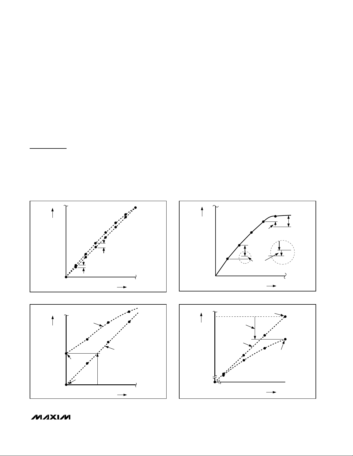
Integral Nonlinearity
Integral nonlinearity (INL) (Figure 5a) is the deviation of
the values on an actual transfer function from either a
best-straight-line fit (closest approximation to the actual
transfer curve) or a line drawn between the endpoints
of the transfer function, once offset and gain errors
have been nullified. For a DAC, the deviations are measured every single step.
Differential Nonlinearity
Differential nonlinearity (DNL) (Figure 5b) is the difference between an actual step height and the ideal value
of 1LSB. A DNL error specification of less than 1LSB
guarantees no missing codes and a monotonic transfer
function.
Offset Error
Offset error (Figure 5c) is the difference between the
ideal and the actual offset point. For a DAC, the offset
point is the step value when the digital input is zero.
This error affects all codes by the same amount and
can usually be compensated by trimming.
Figure 5a. Integral Nonlinearity
Figure 5b. Differential Nonlinearity
Figure 5c. Offset Error
Figure 5d. Gain Error
7
6
5
4
3
ANALOG OUTPUT VALUE
2
1
0
000 010001 011 100 101 110
AT STEP
001 (1/4 LSB )
DIGITAL INPUT CODE
AT STEP
011 (1/2 LSB )
111
6
5
4
3
ANALOG OUTPUT VALUE
2
1
0
000 010001 011 100 101
1 LSB
DIFFERENTIAL
LINEARITY ERROR (+1/4 LSB)
DIGITAL INPUT CODE
DIFFERENTIAL LINEARITY
ERROR (-1/4 LSB)
1 LSB
ACTUAL
OFFSET
POINT
IDEAL OFFSET
POINT
ACTUAL
DIAGRAM
DIGITAL INPUT CODE
3
2
ANALOG OUTPUT VALUE
1
0
000 010001 011
IDEAL DIAGRAM
OFFSET ERROR
(+1 1/4 LSB)
7
6
5
ANALOG OUTPUT VALUE
4
0
000 101100 110 111
IDEAL FULL-SCALE OUTPUT
GAIN ERROR
(-1 1/4 LSB)
IDEAL DIAGRAM
DIGITAL INPUT CODE
ACTUAL
FULL-SCALE
OUTPUT
Page 12

MAX5182/MAX5185
Dual, 10-Bit, 40MHz Current/Voltage
Alternate-Phase Output DACs
12 ______________________________________________________________________________________
Gain Error
Gain error (Figure 5d) is the difference between the
ideal and the actual full-scale output voltage on the
transfer curve, after nullifying the offset error. This error
alters the slope of the transfer function and corresponds to the same percentage error in each step.
Settling Time
Settling time is the amount of time required from the start
of a transition until the DAC output settles its new output
value to within the converter’s specified accuracy.
Digital Feedthrough
Digital feedthrough is the noise generated on a DAC’s
output when any digital input transitions. Proper board
layout and grounding will significantly reduce this
noise, but there will always be some feedthrough
caused by the DAC itself.
Total Harmonic Distortion
Total harmonic distortion (THD) is the ratio of the RMS
sum of the input signal’s first four harmonics to the fundamental itself. This is expressed as:
where V1 is the fundamental amplitude, and V2through
V5are the amplitudes of the 2nd- through 5th-order
harmonics.
Spurious-Free Dynamic Range
Spurious-free dynamic range (SFDR) is the ratio of RMS
amplitude of the fundamental (maximum signal component) to the RMS value of the next-largest distortion
component.
Differential to Single-Ended Conversion
The MAX4108 low-distortion, high-input bandwidth
amplifier may be used to generate a voltage from the
MAX5182’s current array output. The differential voltage
across OUT1P (or OUT2P) and OUT1N (or OUT2N) is
converted into a single-ended voltage by designing an
appropriate operational amplifier configuration as
shown in Figure 6.
Grounding and Power-Supply Decoupling
Grounding and power-supply decoupling strongly influence the performance of the MAX5182/MAX5185.
Unwanted digital crosstalk may couple through the
input, reference, power-supply, and ground connections, which may affect dynamic specifications like signal-to-noise ratio or SFDR. In addition, electromagnetic
interference (EMI) can either couple into or be generated by the MAX5182/MAX5185. Therefore, grounding
and power-supply decoupling guidelines for highspeed, high-frequency applications should be closely
followed.
First, a multilayer PC board with separate ground and
power-supply planes is recommended. High-speed
signals should run on controlled impedance lines
directly above the ground plane. Since the MAX5182/
MAX5185 have separate analog and digital ground
buses (AGND and DGND, respectively), the PC board
should also have separate analog and digital ground
sections with only one point connecting the two. Digital
signals should run above the digital ground, and plane
and analog signals should run above the analog
ground plane.
Both devices have two power-supply inputs: analog
VDD(AVDD) and digital VDD(DVDD). Each AVDDinput
should be decoupled with parallel 10µF and 0.1µF
ceramic chip capacitors as close to the pin as possible. Their opposite ends should have the shortest possible connection to the ground plane. The DVDDpins
should also have separate 10µF and 0.1µF capacitors,
again adjacent to their respective pins. Try to minimize
the analog load capacitance for proper operation. For
best performance, it is recommended to bypass CREF1
and CREF2 with low-ESR 0.1µF capacitors to AVDD.
The power-supply voltages should also be decoupled
at the point they enter the PC board with large tantalum
or electrolytic capacitors. Ferrite beads with additional
decoupling capacitors forming a pi network could also
improve performance.
THD
=×
log
20
VVVV
+++
2232425
V
1
2
Page 13
MAX5182/MAX5185
Dual, 10-Bit, 40MHz Current/Voltage
Alternate-Phase Output DACs
______________________________________________________________________________________ 13
Chip Information
TRANSISTOR COUNT: 9464
SUBSTRATE CONNECTED TO AGND
Figure 6. Differential to Single-Ended Conversion Using a Low-Distortion Amplifier
10µF
R
SET
+3V
+3V
D0–D9
**
0.1µF
0.1µF
AV
CLK
REFO
REFR
AVDDAV
DD
10µF
DD
MAX5182
MAX5185
0.1µF
0.1µF
DV
CREF1
DD
CREF2
OUT1P
OUT1N
OUT2P
OUT2N
REN AGNDDGND
400Ω*
400Ω*
400Ω*
400Ω*
0.1µF
402Ω
402Ω
402Ω
402Ω
402Ω
+5V
OUTPUT1
MAX4108
-5V
402Ω
402Ω
+5V
OUTPUT2
MAX4108
-5V
402Ω
*400Ω RESISTORS INTERNAL TO MAX5185 ONLY.
**MAX5182 ONLY.
Page 14
MAX5182/MAX5185
Dual, 10-Bit, 40MHz Current/Voltage
Alternate-Phase Output DACs
Maxim cannot assume responsibility for use of any circuitry other than circuitry entirely embodied in a Maxim product. No circuit patent licenses are
implied. Maxim reserves the right to change the circuitry and specifications without notice at any time.
14 ____________________Maxim Integrated Products, 120 San Gabriel Drive, Sunnyvale, CA 94086 408-737-7600
© 2001 Maxim Integrated Products Printed USA is a registered trademark of Maxim Integrated Products.
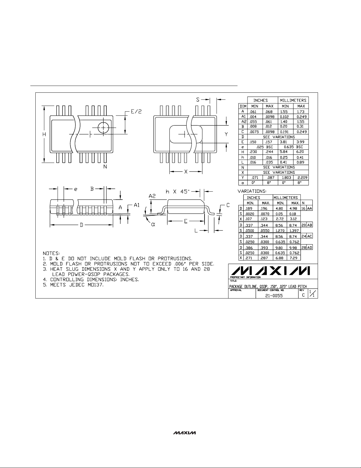
Package Information
QSOP.EPS
 Loading...