

For free samples & the latest literature: http://www.maxim-ic.com, or phone 1-800-998-8800.
For small orders, phone 1-800-835-8769.
General Description
The MAX5175/MAX5177 low-power, serial, voltage-output, 12-bit digital-to-analog converters (DACs) feature a
precision output amplifier in a space-saving 16-pin
QSOP package. The MAX5175 operates from a single
+5V supply, and the MAX5177 operates from a single
+3V supply. The output amplifier’s inverting input is
available to allow specific gain configurations, remote
sensing, and high output current capability. This makes
the MAX5175/MAX5177 ideal for a wide range of applications, including industrial process control. Both
devices draw only 260µA of supply current, which
reduces to 1µA in shutdown mode. In addition, the programmable power-up reset feature allows for a userselectable output voltage state of either 0 or midscale.
The 3-wire serial interface is compatible with SPI™,
QSPI™, and MICROWIRE™ standards. An input register
followed by a DAC register provides a double-buffered
input, allowing the registers to be updated independently or simultaneously with a 16-bit serial word. Additional
features include software and hardware shutdown, shutdown lockout, a hardware reset pin, and a reference
input capable of accepting DC and offset AC signals.
These devices provide a programmable digital output
pin for added functionality and a serial-data output pin
for daisy-chaining. All logic inputs are TTL/CMOS compatible and are internally buffered with Schmitt triggers
to allow direct interfacing to optocouplers.
The MAX5175/MAX5177 incorporate a proprietary on-chip
circuit that keeps the output voltage virtually “glitch free,”
limiting the glitches to a few millivolts during power-up.
Both devices come in 16-pin QSOP packages and are
specified for the extended (-40°C to +85°C) temperature
range. The MAX5171/MAX5173 are 14-bit pin-compatible
upgrades to the MAX5175/MAX5177. For pin-compatible
DACs with an internal reference, see the 13-bit
MAX5132/MAX5133 and 12-bit MAX5122/MAX5123.
Applications
Digitally Programmable 4–20mA Current Loops
Industrial Process Controls
Digital Offset and Gain Adjustment
Motion Control
Automatic Test Equipment (ATE)
Remote Industrial Controls
µP-Controlled Systems
Features
♦ ±1 LSB INL
♦ 1µA Shutdown Current
♦ “Glitch Free” Output Voltage at Power-Up
♦ Single-Supply Operation
+5V (MAX5175)
+3V (MAX5177)
♦ Full-Scale Output Range
+2.048V (MAX5177, V
REF
= +1.25V)
+4.096V (MAX5175, V
REF
= +2.5V)
♦ Rail-to-Rail®Output Amplifier
♦ Adjustable Output Offset
♦ Low THD (-80dB) in Multiplying Operation
♦ SPI/QSPI/MICROWIRE-Compatible 3-Wire
Serial Interface
♦ Programmable Shutdown Mode and Power-Up
Reset (0 or midscale)
♦ Buffered Output Capable of Driving 4–20mA or
5kΩ || 100pF Loads
♦ User-Programmable Digital Output Pin Allows
Serial Control of External Components
♦ 14-Bit Upgrades Available (MAX5171/MAX5173)
MAX5175/MAX5177
Low-Power, Serial, 12-Bit DACs with
Force/Sense Voltage Output
________________________________________________________________
Maxim Integrated Products
1
16
15
14
13
12
11
10
9
1
2
3
4
5
6
7
8
FB V
DD
N.C.
REF
AGND
SHDN
UPO
DOUT
DGND
TOP VIEW
MAX5175
MAX5177
QSOP
OUT
RS
CS
PDL
CLR
DIN
SCLK
19-1477; Rev 0; 4/99
PART
MAX5175AEEE
MAX5175BEEE
MAX5177AEEE
-40°C to +85°C
-40°C to +85°C
-40°C to +85°C
TEMP. RANGE PIN-PACKAGE
16 QSOP
16 QSOP
16 QSOP
Functional Diagram appears at end of data sheet.
Pin Configuration
Ordering Information
MAX5177BEEE -40°C to +85°C 16 QSOP
INL
(LSB)
±1
±2
±2
±4
SPI and QSPI are trademarks of Motorola, Inc.
MICROWIRE is a trademark of National Semiconductor Corp.
Rail-to-Rail is a registered trademark of Nippon Motorola, Ltd.
LSB
MAX5175/MAX5177
Low-Power, Serial, 12-Bit DACs with
Force/Sense Voltage Output
2 _______________________________________________________________________________________
ABSOLUTE MAXIMUM RATINGS
ELECTRICAL CHARACTERISTICS—MAX5175
(VDD= +5V ±10%, V
REF
= 2.5V, AGND = DGND, FB = OUT, RL= 5kΩ, CL= 100pF referenced to ground, TA= T
MIN
to T
MAX
, unless
otherwise noted. Typical values are at T
A
= +25°C.)
Stresses beyond those listed under “Absolute Maximum Ratings” may cause permanent damage to the device. These are stress ratings only, and functional
operation of the device at these or any other conditions beyond those indicated in the operational sections of the specifications is not implied. Exposure to
absolute maximum rating conditions for extended periods may affect device reliability.
VDDto AGND, DGND...............................................-0.3V to +6V
AGND to DGND.....................................................-0.3V to +0.3V
Digital Inputs to DGND.............................................-0.3V to +6V
DOUT, UPO to DGND ................................-0.3V to (V
DD
+ 0.3V)
FB, OUT REF to AGND...............................-0.3V to (V
DD
+ 0.3V)
Maximum Current into Any Pin............................................50mA
Continuous Power Dissipation (T
A
= +70°C)
16-Pin QSOP (derate 8mW/°C above +70°C)...............667mW
Operating Temperature Range.............................-40°C to +85°C
Storage Temperature Range.............................-65°C to +150°C
Lead Temperature (soldering, 10sec).............................+300°C
CONDITIONS UNITSMIN TYP MAXSYMBOLPARAMETER
Bits12Resolution
MAX5175A ±1
MAX5175B
LSB
±2
INLIntegral Nonlinearity (Note 1)
LSB±1DNLDifferential Nonlinearity
mV±10V
OS
Offset Error (Note 2)
RL= ∞
-0.6 ±4
GEGain Error
RL= 5kΩ
LSB
-1.6 ±8
µV/V10 120PSRRPower-Supply Rejection Ratio
f = 100kHz LSBp-p1Output Noise Voltage
nV/√Hz
50Output Thermal Noise Density
V0V
DD
- 1.4V
REF
Reference Input Range
kΩ18R
REF
Reference Input Resistance
V
REF
= 0.5Vp-p + 2.5VDC, slew-rate limited kHz350Reference -3dB Bandwidth
V
REF
= 1.4Vp-p + 2.5VDC, f = 10kHz,
code = FFF hex
dB84SINAD
Signal-to-Noise Plus Distortion
Ratio
V3V
IH
Input High Voltage
V0.8V
IL
Input Low Voltage
mV200V
HYS
Input Hysteresis
VIN= 0 or V
DD
µA0.001 ±1I
IN
Input Leakage Current
pF8C
IN
Input Capacitance
I
SOURCE
= 2mA VVDD- 0.5V
OH
Output High Voltage
I
SINK
= 2mA V0.13 0.4V
OL
Output Low Voltage
V
REF
= 3.6Vp-p + 1.8VDC, f = 1kHz,
code = all 0s
dB-84Reference Feedthrough
STATIC PERFORMANCE
REFERENCE INPUT
MULTIPLYING-MODE PERFORMANCE
DIGITAL INPUTS
DIGITAL OUTPUTS
MAX5175/MAX5177
Low-Power, Serial, 12-Bit DACs with
Force/Sense Voltage Output
_______________________________________________________________________________________ 3
ELECTRICAL CHARACTERISTICS—MAX5175 (continued)
(VDD= +5V ±10%, V
REF
= 2.5V, AGND = DGND, FB = OUT, RL= 5kΩ, CL= 100pF referenced to ground, TA= T
MIN
to T
MAX
, unless
otherwise noted. Typical values are at T
A
= +25°C.)
CONDITIONS
V/µs0.6SRVoltage Output Slew Rate
V0 V
DD
Output Voltage Swing (Note 3)
µA-0.1 0 0.1Current into FB
µs40Time Required to Exit Shutdown
UNITSMIN TYP MAXSYMBOLPARAMETER
CS = VDD; f
SCLK
= 100kHz, V
SCLK
= 5Vp-p
nV-s1Digital Feedthrough
V4.5 5.5V
DD
Positive Supply Voltage
mA0.26 0.35I
DD
Power-Supply Current (Note 4)
µA110Shutdown Current (Note 4)
ns100t
CP
SCLK Clock Period
ns40t
CH
SCLK Pulse Width High
ns40t
CL
SCLK Pulse Width Low
ns40t
CSS
CS Fall to SCLK Rise Setup
Time
ns40t
DS
SDI Setup Time
ns0t
DH
SDI Hold Time
C
LOAD
= 200pF ns80t
DO1
SCLK Rise to DOUT Valid
Propagation Delay
C
LOAD
= 200pF ns80t
DO2
SCLK Fall to DOUT Valid
Propagation Delay
ns10t
CS0
SCLK Rise to CS Fall Delay
ns100t
CSW
CS Pulse Width High
ns0t
CSH
SCLK Rise to CS Rise Hold
Time
ns40t
CS1
CS Rise to SCLK Rise Hold Time
To ±0.5LSB, from 10mV to full-scale µs12Output Settling Time
DYNAMIC PERFORMANCE
POWER SUPPLIES
TIMING CHARACTERISTICS
LSB
MAX5175/MAX5177
Low-Power, Serial, 12-Bit DACs with
Force/Sense Voltage Output
4 _______________________________________________________________________________________
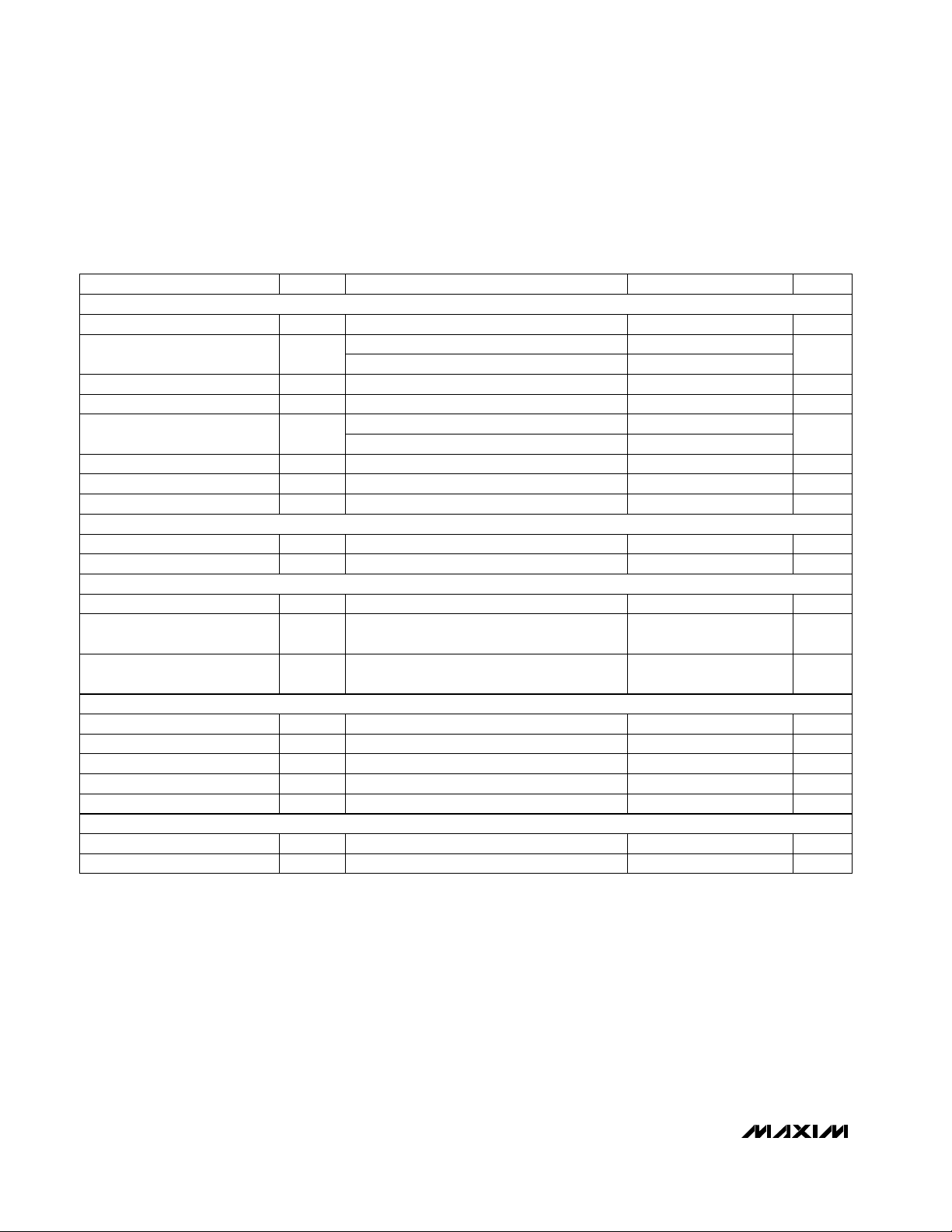
ELECTRICAL CHARACTERISTICS—MAX5177
(VDD= +2.7V to +3.6V, V
REF
= 1.25V, AGND = DGND, FB = OUT, RL= 5kΩ, CL= 100pF referenced to ground, TA= T
MIN
to T
MAX
,
unless otherwise noted. Typical values are at T
A
= +25°C.)
Bits12Resolution
MAX5177A ±2
V
REF
= 1.6Vp-p + 0.8VDC, f = 1kHz,
code = all 0s
dB
MAX5177B
LSB
±4
INLIntegral Nonlinearity (Note 5)
LSB±1DNLDifferential Nonlinearity
mV±10
CONDITIONS
V
OS
Offset Error (Note 2)
RL= ∞
-0.6 ±4
GEGain Error
RL= 5kΩ
LSB
-1.6 ±8
-84
µV/V10 120PSRRPower-Supply Rejection Ratio
f = 100kHz LSBp-p2Output Noise Voltage
nV/√Hz
50Output Thermal Noise Density
V0V
DD
- 1.4V
REF
Reference Input Range
kΩ18R
REF
Reference Input Resistance
V
REF
= 0.5Vp-p + 1.25VDC, slew-rate limited kHz350Reference -3dB Bandwidth
V
REF
= 0.9Vp-p + 1.25VDC, f = 10kHz,
code = FFF hex
dB78SINAD
Signal-to-Noise Plus Distortion
Ratio
Reference Feedthrough
V2.2V
IH
Input High Voltage
V0.8V
IL
Input Low Voltage
mV200V
HYS
Input Hysteresis
VIN= 0 or V
DD
µA0.001 ±1I
IN
Input Leakage Current
UNITSMIN TYP MAXSYMBOLPARAMETER
pF8C
IN
Input Capacitance
I
SOURCE
= 2mA VVDD- 0.5V
OH
Output High Voltage
I
SINK
= 2mA V0.13 0.4V
OL
Output Low Voltage
STATIC PERFORMANCE
REFERENCE
MULTIPLYING-MODE PERFORMANCE
DIGITAL INPUTS
DIGITAL OUTPUTS
MAX5175/MAX5177
Low-Power, Serial, 12-Bit DACs with
Force/Sense Voltage Output
_______________________________________________________________________________________ 5
Note 1: INL guaranteed between codes 16 and 4095.
Note 2: Offset is measured at the code that comes closest to 10mV.
Note 3: Accuracy is better than 1LSB for V
OUT
= 10mV to VDD- 180mV. Guaranteed by PSR test on end points.
Note 4: R
L
= open and digital inputs are either VDDor DGND.
Note 5: INL guaranteed between codes 32 and 4095.
ELECTRICAL CHARACTERISTICS—MAX5177 (continued)
(VDD= +2.7V to +3.6V, V
REF
= 1.25V, AGND = DGND, FB = OUT, RL= 5kΩ, CL= 100pF referenced to ground, TA= T
MIN
to T
MAX
,
unless otherwise noted. Typical values are at TA= +25°C.)
µA110Shutdown Current (Note 4)
ns150t
CP
SCLK Clock Period
ns75t
CH
SCLK Pulse Width High
ns75
CONDITIONS
t
CL
SCLK Pulse Width Low
ns60t
CSS
CS Fall to SCLK Rise Setup
Time
ns0t
CSH
SCLK Rise to CS Rise Hold
Time
ns60t
DS
SDI Setup Time
ns0t
DH
SDI Hold Time
C
LOAD
= 200pF ns200t
DO1
SCLK Rise to DOUT Valid
Propagation Delay
ns75t
CS1
CS Rise to SCLK Rise Hold Time
C
LOAD
= 200pF ns200t
DO2
SCLK Fall to DOUT Valid
Propagation Delay
To ±0.5LSB, from 10mV to full-scale µs12Output Settling Time
ns10t
CS0
SCLK Rise to CS Fall Delay
ns150t
CSW
CS Pulse Width High
V/µs0.6SRVoltage Output Slew Rate
V0V
DD
Output Voltage Swing (Note 3)
µA-0.1 0 0.1Current into FB
µs40Time Required to Exit Shutdown
UNITSMIN TYP MAXSYMBOLPARAMETER
CS = VDD, DIN = 50kHz, f
SCLK
= 100kHz,
V
SCLK
= 3Vp-p
nV-s1Digital Feedthrough
V2.7 3.6V
DD
Positive Supply Voltage
mA0.26 0.35I
DD
Power-Supply Current (Note 4)
DYNAMIC PERFORMANCE
POWER SUPPLIES
TIMING CHARACTERISTICS

MAX5175/MAX5177
Low-Power, Serial, 12-Bit DACs with
Force/Sense Voltage Output
6 _______________________________________________________________________________________
Typical Operating Characteristics
(MAX5175: VDD= +5V, V
REF
= 2.5V; MAX5177: VDD= +3V, V
REF
= 1.25V; CL = 100pF, FB = OUT, code = FFF hex, TA= +25°C,
unless otherwise noted.)
210
240
230
220
250
260
270
280
290
300
310
4.4 4.84.6 5.0 5.2 5.4 5.6
NO-LOAD SUPPLY CURRENT
vs. SUPPLY VOLTAGE
MAX5175-01
SUPPLY VOLTAGE (V)
NO-LOAD SUPPLY CURRENT (µA)
248
252
250
258
256
254
264
262
260
266
-50 -10 10-30 30 50 70 90
NO-LOAD SUPPLY CURRENT
vs. TEMPERATURE
MAX5175-02
TEMPERATURE (°C)
NO-LOAD SUPPLY CURRENT (µA)
0.8
1.0
0.9
1.2
1.1
1.3
1.4
-50 10 30-30 -10 50 70 90
SHUTDOWN SUPPLY CURRENT
vs. TEMPERATURE
MAX5175-03
TEMPERATURE (°C)
SHUTDOWN SUPPLY CURRENT (µA)
2.49930
2.49934
2.49938
2.49942
2.49946
2.49950
-50 -10 10-30 30 50 70 90
OUTPUT VOLTAGE vs. TEMPERATURE
MAX5175-04
TEMPERATURE (°C)
OUTPUT VOLTAGE (V)
V
OUT
(1V/div)
V
CS
(5V/div)
5V
2.5V
10mV
0
2µs/div
DYNAMIC RESPONSE
MAX5175-07
10k 100k
0
0.5
1.0
1.5
2.0
2.5
3.0
10 100 1k
OUTPUT VOLTAGE vs. LOAD RESISTANCE
MAX5175-05
RL (Ω)
OUTPUT VOLTAGE (V)
V
OUT
(1V/div)
V
CS
(5V/div)
5V
2.5V
10mV
0
2µs/div
DYNAMIC RESPONSE
MAX5175-06
10k 100k
-92
-90
-88
-86
-84
-82
-80
-78
10 100 1k
TOTAL HARMONIC DISTORTION
PLUS NOISE vs. FREQUENCY
MAX5175-08
FREQUENCY (Hz)
THD + NOISE (dB)
V
OUT/VREF
(12.5dB/div)
20
0
10k
REFERENCE FEEDTHROUGH
MAX5175 toc9
FREQUENCY (Hz)
V
REF
= 1.8VDC + 3.6Vp-p at f = 1kHz
MAX5175

MAX5175/MAX5177
Low-Power, Serial, 12-Bit DACs with
Force/Sense Voltage Output
_______________________________________________________________________________________
7
V
OUT/VREF
(12.5dB/div)
20
0
100k
FFT PLOT
MAX5175 toc10
FREQUENCY (Hz)
V
REF
= 2.5 VDC + 1.414Vp-p at f = 10kHz
V
OUT
(100mV/div)
V
CS
(2V/div)
MAJOR-CARRY TRANSITION
MAX5175-11
V/SCLK
(5V/div)
400ns/div
V
OUT
(2mV/div)
DIGITAL FEEDTHROUGH
MAX5175-12
AC-COUPLED
-25
-20
-10
-15
-5
0
0 1000500 1500 2000 2500 3000
REFERENCE INPUT FREQUENCY RESPONSE
MAX5175-13
FREQUENCY (kHz)
GAIN (dB)
V
REF
= 0.67Vp-p + 1.25V
DC
252
256
254
260
258
266
264
262
268
-50 -10-30 10 30 50 70 90
NO-LOAD SUPPLY CURRENT
vs. TEMPERATURE
MAX5175-16
TEMPERATURE (°C)
NO-LOAD SUPPLY CURRENT (µA)
V
OUT
(10mV/div)
V
DD
(1V/div)
50ms/div
START-UP GLITCH
MAX5175-14
AC-COUPLED
230
240
235
250
245
260
255
265
275
270
280
2.5 2.7 2.8 2.92.6 3.0 3.1 3.2 3.43.3 3.5
NO-LOAD SUPPLY CURRENT
vs. SUPPLY VOLTAGE
MAX5175-15
SUPPLY VOLTAGE (V)
NO-LOAD SUPPLY CURRENT (µA)
0.44
0.48
0.46
0.52
0.50
0.58
0.56
0.54
0.60
-50 -10-30 10 30 50 70 90
SHUTDOWN SUPPLY CURRENT
vs. TEMPERATURE
MAX5175-17
TEMPERATURE (°C)
SHUTDOWN SUPPLY CURRENT (µA)
Typical Operating Characteristics (continued)
(MAX5175: VDD= +5V, V
REF
= 2.5V; MAX5177: VDD= +3V, V
REF
= 1.25V; CL = 100pF, FB = OUT, code = FFF hex, TA= +25°C,
unless otherwise noted.)
MAX5175
MAX5177

MAX5175/MAX5177
Low-Power, Serial, 12-Bit DACs with
Force/Sense Voltage Output
8 _______________________________________________________________________________________
Typical Operating Characteristics (continued)
(MAX5175: VDD= +5V, V
REF
= 2.5V; MAX5177: VDD= +3V, V
REF
= 1.25V; CL = 100pF, FB = OUT, code = FFF hex, TA= +25°C,
unless otherwise noted.)
10k 100k
0
0.2
0.4
0.8
0.6
1.0
1.2
1.4
10 100 1k
OUTPUT VOLTAGE vs. RESISTANCE LOAD
MAX5175-19
RL (Ω)
OUTPUT VOLTAGE (V)
V
OUT
(500mV/div)
V
CS
(3V/div)
3V
1.25V
10mV
0
2µs/div
DYNAMIC RESPONSE
MAX5175-20
V
OUT
(500mV/div)
V
CS
(3V/div)
3V
1.25V
10mV
0
2µs/div
DYNAMIC RESPONSE
MAX5175-21
10k 100k
-88
-84
-86
-82
-78
-80
-74
-76
-72
10 100 1k
TOTAL HARMONIC DISTORTION
PLUS NOISE vs. FREQUENCY
MAX5175-22
FREQUENCY (Hz)
THD + NOISE (dB)
V
OUT/VREF
(12.5dB/div)
20
0
10k
REFERENCE FEEDTHROUGH
MAX5175 toc23
FREQUENCY (Hz)
V
REF
= 0.8VDC + 1.6Vp-p at f = 1kHz
V
OUT/VREF
(12.5dB/div)
20
0
100k
FFT PLOT
MAX5175 toc24
FREQUENCY (Hz)
V
REF
= 1.5VDC + 0.848V
p-p
at f = 10kHz
OUT
(500µV/div)
2µs/div
SCLK
(2V/div)
DIGITAL FEEDTHROUGH (SCLK, OUT)
MAX5175/77 toc26
AC-COUPLED
MAX5177
1.24930
1.24940
1.24950
1.24960
1.24970
1.24980
-50 -10 10-30 30 50 70 90
OUTPUT VOLTAGE vs. TEMPERATURE
MAX5175-18
TEMPERATURE (°C)
OUTPUT VOLTAGE (V)
V
OUT
(100mV/div)
5µs/div
MAJOR-CARRY TRANSITION
MAX5175/77 toc25
V
CS
(2V/div)
AC-COUPLED

MAX5175/MAX5177
Low-Power, Serial, 12-Bit DACs with
Force/Sense Voltage Output
_______________________________________________________________________________________ 9
Pin Description
Typical Operating Characteristics (continued)
(MAX5175: VDD= +5V, V
REF
= 2.5V; MAX5177: VDD= +3V, V
REF
= 1.25V; CL = 100pF, FB = OUT, code = FFF hex, TA= +25°C,
unless otherwise noted.)
V
OUT
(10mV/div)
AC-COUPLED
V
DD
(1V/div)
50ms/div
START-UP GLITCH
MAX5175-28
PIN
Feedback Input FB1
FUNCTIONNAME
Voltage Output. High impedance in shutdown. Output voltage is limited to VDD.OUT2
Power-Down Lockout (digital input). Connect to VDDto allow shutdown. Connect to DGND to disable shutdown.
PDL
4
Reset Mode Select (digital input). Connect to VDDto select midscale reset output value. Connect to DGND
to select 0 reset output value.
RS3
Chip-Select Input (digital input). DIN is ignored when CS is high.CS
6
Serial Clock Input (digital input)SCLK8
Serial-Data Input (digital input). Data is clocked in on the rising edge of SCLK.DIN7
Clear DAC (digital input). Clears the DAC to its predetermined output state as set by RS.
CLR
5
Serial-Data OutputDOUT10
Shutdown (digital input). Pulling SHDN high when PDL = VDDplaces the chip in shutdown with a maximum
shutdown current of 10µA.
SHDN12
User-Programmable Output. State is set by the serial input.UPO11
Reference Input. Maximum V
REF
is VDD- 1.4V.REF14
Positive Supply. Bypass to AGND with a 4.7µF capacitor in parallel with a 0.1µF capacitor.V
DD
16
No ConnectN.C.15
Analog GroundAGND13
Digital GroundDGND9
MAX5177
REFERENCE INPUT FREQUENCY RESPONSE
0
-5
-10
GAIN (dB)
-15
-20
V
-25
0 1000500 1500 2000 2500 3000
MAX5175-27
= 0.67Vp-p + 1.25V
REF
DC
FREQUENCY (kHz)

MAX5175/MAX5177
Low-Power, Serial, 12-Bit DACs with
Force/Sense Voltage Output
10 ______________________________________________________________________________________
Detailed Description
The MAX5175/MAX5177 12-bit, serial, voltage-output
DACs operate with a 3-wire serial interface. These
devices include a 16-bit shift register and a doublebuffered input composed of an input register and a
DAC register (see
Functional Diagram
). In addition, the
negative terminal of the output amplifier is available.
The DACs are designed with an inverted R-2R ladder
network (Figure 1) that produces a weighted voltage
proportional to the reference voltage.
Reference Inputs
The reference input accepts both AC and DC values with
a voltage range extending from 0 to VDD- 1.4V. The following equation represents the resulting output voltage:
where N is the numeric value of the DAC’s binary input
code (0 to 4095), V
REF
is the reference voltage, and
Gain is the externally set voltage gain. The maximum
output voltage is VDD. The reference pin has a minimum impedance of 18kΩ and is code dependent.
Output Amplifier
The MAX5175/MAX5177’s DAC output is internally
buffered by a precision amplifier with a typical slew rate
of 0.6V/µs. Access to the output amplifier’s inverting
input provides flexibility in output gain setting and signal conditioning (see
Applications Information
).
The output amplifier settles to ±0.5LSB from a full-scale
transition within 12µs, when loaded with 5kΩ in parallel
with 100pF. Loads less than 2kΩ degrade performance.
Shutdown Mode
The MAX5175/MAX5177 feature a software- and hardware-programmable shutdown mode that reduces the
typical supply current to 1µA. Enter shutdown by writing
the appropriate input-control word as shown in Table 1
or by using the hardware shutdown function. In shutdown mode, the reference input and the amplifier output become high impedance and the serial interface
remains active. Data in the input register is saved,
allowing the MAX5175/MAX5177 to recall the prior output state when returning to normal operation. Exit shutdown by reloading the DAC register from the shift
register, by simultaneously loading the input and DAC
registers, or by toggling PDL. When returning from
shutdown, wait 40µs for the output to settle.
Power-Down Lockout
Power-down lockout disables the software/hardware
shutdown mode. A high-to-low transition on PDL brings
the device out of shutdown, returning the output to its
previous state.
Shutdown
Pulling SHDN high while PDL is high places the
MAX5175/MAX5177 in shutdown. Pulling SHDN low does
not take the device out of shutdown. A high-to-low transition on PDL or an appropriate command from the serial
data line (see Table 1 for commands) is required to exit
shutdown.
Serial Interface
The 3-wire serial interface is compatible with SPI, QSPI
(Figure 2), and MICROWIRE (Figure 3) interface standards. The 16-bit serial input word consists of two control bits, 12 bits of data (MSB to LSB), and two sub-bits.
The control bits determine the MAX5175/MAX5177’s
response as outlined in Table 1. The digital inputs are
double buffered, which allows any of the following:
• Loading the input register without updating the DAC
register
• Updating the DAC register from the input register
• Updating the input and DAC registers simultaneously.
V
V N GAIN
4096
OUT
REF
=
⋅⋅
OUT
FB
SHOWN FOR ALL 1s ON DAC
MSB
2R
2R 2R 2R 2R
RRR
REF
AGND
Figure 1. Simplified DAC Circuit Diagram

MAX5175/MAX5177
Low-Power, Serial, 12-Bit DACs with
Force/Sense Voltage Output
______________________________________________________________________________________ 11
The MAX5175/MAX5177 accept one 16-bit packet or
two 8-bit packets sent while CS remains low. The
devices allow the following to be configured:
• Clock edge on which serial data output (DOUT) is
clocked out
• State of the user-programmable logic output
• Reset state.
Specific commands for setting these are shown in
Table 1.
The general timing diagram in Figure 4 illustrates how
the MAX5175/MAX5177 acquire data. CS must go low
at least t
CSS
before the rising edge of the serial clock
(SCLK). With CS low, data is clocked into the register
on the rising edge of SCLK. The maximum serial clock
frequency guaranteed for proper operation is 10MHz
for the MAX5175 and 6MHz for the MAX5177. See
Figure 5 for a detailed timing diagram of the serial interface.
Table 1. Serial-Interface Programming Commands
Load input register; DAC registers are updated (start up DAC with
new data).
10
Load input register; DAC registers are unchanged.00
12-bit DAC data
12-bit DAC data
00
00
16-BIT SERIAL WORD
D11..................D0 S1, S0C1
FUNCTION
C0
No operation (NOP).11 0 0 x x xxxx xxxx
xxxx xxxx xxxx
xx
xx
Update DAC register from input register (start up DAC with data
previously stored in the input registers).
01
UPO goes low (default).11 1 0 0 x xxxx xxxx
0 1 x x xxxx xxxx
xx
xx
Mode 1, DOUT clocked out on SCLK’s rising edge.11 1 1 0 x xxxx xxxx
1 0 1 x xxxx xxxx
xx
xx UPO goes high.11
Shut down DAC (provided PDL = 1).
11
Mode 0, DOUT clocked out on SCLK’s falling edge (default).11 1 1 1 x xxxx xxxx xx
Figure 2. Connections for SPI/QSPI Standards
SCLK
DIN
CS
SK
SO
I/O
SPI/QSPI
PORT
CPOL = 0, CPHA = 0
MAX5175
MAX5177
Figure 3. Connections for MICROWIRE
DIN
MAX5175
MAX5177
SCLK
CS
MOSI
MICROWIRE
SCK
I/O
CPOL = 0, CPHA = 0
PORT
+5V
SS

MAX5175/MAX5177
Low-Power, Serial, 12-Bit DACs with
Force/Sense Voltage Output
12 ______________________________________________________________________________________
Serial-Data Output (DOUT)
The serial-data output (DOUT) is the internal shift register’s output and allows for daisy-chaining of multiple
devices as well as data readback (see
Applications
Information
). By default upon start-up, data shifts out of
DOUT on the serial clock’s rising edge (Mode 0) and
provides a lag of 16 clock cycles, thus maintaining SPI,
QSPI, and MICROWIRE compatibility. However, if the
device is programmed for Mode 1, then the output data
lags DIN by 16.5 clock cycles and is clocked out on the
serial clock’s rising edge. During shutdown, DOUT
retains its last digital state prior to shutdown.
User-Programmable Logic Output (UPO)
The UPO allows control of an external device through
the serial interface, thereby reducing the number of
microcontroller I/O pins required. During power-down,
this output will retain its digital state prior to shutdown.
When CLR is pulled low, UPO will reset to its programmed default state. See Table 1 for specific commands to control the UPO.
Reset (RS) and Clear (
CCLLRR
)
The MAX5175/MAX5177 offers a clear pin (CLR) which
resets the output voltage. If RST = DGND, then CLR
resets the output voltage to the minimum voltage (0 if
no offset is introduced). If RST = VDD, then CLR resets
the output voltage to midscale. In either case, CLR will
reset UPO to its programmed default state.
CS
SCLK
DIN
COMMAND
EXECUTED
9
8
16
1
C1
C2 S0
C0
D9
D8
D7
D6 D3 D2 D1 D0 S2 S1D5 D4
Figure 4. Serial-Interface Timing Diagram
CS
SCLK
DIN
DOUT
t
CSW
t
CS1
t
CSH
t
CSS
t
CSO
t
D02
t
CH
t
CL
t
CP
t
D01
t
DS
t
DH
Figure 5. Detailed Serial-Interface Timing Diagram

Applications Information
Unipolar Output
Figure 6 shows the MAX5175/MAX5177 configured for
unipolar, rail-to-rail operation with a gain of +2V/V.
Table 2 lists the codes for unipolar output voltages. The
output voltage is limited to VDD.
Bipolar Output
Figure 7 shows the MAX5175/MAX5177 configured for
bipolar output operation. The output voltage is given by
the following equation (FB = OUT):
where N represents the numeric value of the DAC’s
binary input code and V
REF
is the voltage of the external reference. Table 3 shows digital codes and the corresponding output voltage for Figure 7’s circuit.
Daisy-Chaining Devices
The serial data output pin (DOUT) allows multiple
MAX5175/MAX5177s to be daisy-chained together as
shown in Figure 8. The advantage of this is that only
two lines are needed to control all of the DACs on the
line. The disadvantage is that it takes ncommands to
program the DACs. Figure 9 shows several MAX5175/
MAX5177s sharing one common DIN signal line. In this
configuration the data bus is common to all devices;
however, more I/O lines are required because each
device needs a dedicated CS line. The advantage of
this configuration is that only one command is needed
to program any DAC.
V V
2N
4096
1
OUT REF
=−
MAX5175/MAX5177
Low-Power, Serial, 12-Bit DACs with
Force/Sense Voltage Output
______________________________________________________________________________________ 13
Table 2. Unipolar Code Table (Circuit of
Figure 6)
11 1111 1111 11 (00)
2 · V
REF
(4095/4096)
10 0000 0000 01 (00)
2 · V
REF
(2049/4096)
01 1111 1111 11 (00)
10 0000 0000 00 (00)
2 · V
REF
(2047/4096)
2 · V
REF
(2048/4096)
00 0000 0000 00 (00)
00 0000 0000 01 (00)
0
2 · V
REF
(1/4096)
ANALOG OUTPUT
DAC CONTENTS
MSB LSB
Figure 6. Unipolar Output Circuit (Rail-to-Rail)
DAC
V
OUT
V+
V-
+5V/+3.3V
R1 = R2 = 10kΩ ± 0.1%
MAX5175
MAX5177
REF
10k
10k
FB
OUT
V
DD
GND
Figure 7. Bipolar Output Circuit
Table 3. Bipolar Code Table (Circuit of
Figure 7)
11 1111 1111 11 (00)
ANALOG OUTPUT
+V
REF
[(2 · 4095/4096) - 1]
10 0000 0000 01 (00)
+V
REF
[(2 · 2049/4096) - 1]
01 1111 1111 11 (00)
10 0000 0000 00 (00)
+V
REF
[(2 · 2047/4096) - 1]
+V
REF
[(2 · 2048/4096) - 1]
DAC CONTENTS
MSB LSB
00 0000 0000 00 (00)
00 0000 0000 01 (00)
-V
REF
+V
REF
[(2 · 1/4096) - 1]
MAX5175
MAX5177
REF
DAC
+5V/+3.3V
V
DD
FB
OUT
10k
10k
GND

MAX5175/MAX5177
Low-Power, Serial, 12-Bit DACs with
Force/Sense Voltage Output
14 ______________________________________________________________________________________
TO OTHER
SERIAL DEVICES
MAX5175
MAX5177
DIN
SCLK
CS
MAX5175
MAX5177
MAX5175
MAX5177
DINDOUT DOUT DOUT
SCLK
CS
DIN
SCLK
CS
Figure 8. Daisy-Chaining MAX5175/MAX5177s
TO OTHER
SERIAL DEVICES
MAX5175
MAX5177
DIN
SCLK
CS
MAX5175
MAX5177
DIN
SCLK
CS
MAX5175
MAX5177
DIN
SCLK
CS
DIN
SCLK
CS1
CS2
CS3
Figure 9. Multiple MAX5175/MAX5177s Sharing Common DIN and SCLK Lines

MAX5175/MAX5177
Low-Power, Serial, 12-Bit DACs with
Force/Sense Voltage Output
______________________________________________________________________________________ 15
Using an AC Reference
The MAX5175/MAX5177 accept reference voltages
containing AC components, as long as the reference
voltage remains between 0 and VDD- 1.4V. Figure 10
shows a technique for applying a sine-wave signal to
REF. The reference voltage must remain above AGND.
Digitally Programmable
Current Source
The circuit of Figure 11 places an NPN transistor
(2N3904 or similar) within the op amp feedback loop to
implement a digitally programmable, unidirectional current source. The output current is calculated with the
following equation:
where N is the numeric value of the DAC’s binary input
code and R is the sense resistor shown in Figure 11.
Power-Supply and Layout Considerations
Wire-wrap boards are not recommended. For optimum
system performance, use printed circuit boards with
separate analog and digital ground planes. Connect
the two ground planes together at the low-impedance
power-supply source. Connect DGND and AGND pins
together at the IC. The best ground connection is
achieved by connecting the DAC’s DGND and AGND
pins together and connecting that point to the system
analog ground plane. If the DAC’s DGND is connected
to the system digital ground, digital noise may infiltrate
the DAC’s analog portion.
Bypass the power supply with a 4.7µF capacitor in parallel with a 0.1µF capacitor to AGND. Minimize capacitor lead lengths to reduce inductance. If noise
becomes an issue, use shielding and/or ferrite beads to
increase isolation.
In order to maintain INL and DNL performance, as well
as gain drift, it is extremely important to provide the
lowest possible reference output impedance at the
DAC reference input pin. INL degrades if the series
resistance on the REF pin exceeds 0.1Ω. The same
consideration must be made for the AGND pin.
DAC
OUT
MAX5175
MAX5177
R
1
R
1
REF
V
DD
GND
+5V/
+3.3V
+5V/+3.3V
AC
REFERENCE
INPUT
500mVp-p
MAX495
Figure 10. AC Reference Input Circuit
DAC
MAX5175
MAX5177
REF
OUT
R
I
OUT
2N3904
V
L
FB
+5V/+3.3V
V
DD
GND
Figure 11. Digitally Programmable Current Source
I
V N
R 4096
OUT
REF
=
⋅
⋅

MAX5175/MAX5177
Low-Power, Serial, 12-Bit DACs with
Force/Sense Voltage Output
Maxim cannot assume responsibility for use of any circuitry other than circuitry entirely embodied in a Maxim product. No circuit patent licenses are
implied. Maxim reserves the right to change the circuitry and specifications without notice at any time.
16
____________________Maxim Integrated Products, 120 San Gabriel Drive, Sunnyvale, CA 94086 408-737-7600
© 1999 Maxim Integrated Products Printed USA is a registered trademark of Maxim Integrated Products.
Package Information
QSOP.EPS
MAX5175
MAX5177
DOUT
UPO
FB
OUT
RS
SHDN
PDL
CLR
DAC
16-BIT
SHIFT
REGISTER
DAC
REGISTER
REF
INPUT
REGISTER
DECODE
CONTROL
LOGIC
OUTPUT
SERIAL
CONTROL
V
DD
AGND
DGND
CS
DIN
SCLK
Functional Diagram Chip Information
TRANSISTOR COUNT: 3457
 Loading...