

Page 1
General Description
The MAX5134 is a low-power, quad 16-bit, buffered voltage-output, high-linearity digital-to-analog converter
(DAC). It uses a precision internal reference or a precision external reference for rail-to-rail operation. The
MAX5134 accepts a wide +2.7V to +5.25V supply-voltage range to accommodate most low-power and lowvoltage applications. The device accepts a 3-wire
SPITM-/QSPITM-/MICROWIRETM-/DSP-compatible serial
interface to save board space and reduce the complexity of optically isolated and transformer-isolated applications. The digital interface’s double-buffered hardware
and software LDAC provide simultaneous output update.
The serial interface features a READY output for easy
daisy-chaining of several MAX5134 devices and/or other
compatible devices. The MAX5134 includes a hardware
input to power-up or reset the DAC outputs to zero or
midscale, providing additional safety for applications that
drive valves or other transducers that need to be off during power-up. The high linearity of the DACs makes
these devices ideal for precision control and instrumentation applications. The MAX5134 is available in an ultrasmall (4mm x 4mm), 24-pin TQFN package and is
specified over the -40°C to +105°C extended industrial
temperature range.
Applications
Automatic Test Equipment
Automatic Tuning
Communication Systems
Data Acquisition
Gain and Offset Adjustment
Portable Instrumentation
Power-Amplifier Control
Process Control and Servo Loops
Programmable Voltage and Current Sources
Features
♦ 16-Bit Resolution in a 4mm x 4mm, 24-Pin TQFN
Package
♦ Hardware-Selectable Power-Up or Reset-to-Zero/
Midscale DAC Output
♦ Double-Buffered Input Registers
♦ LDAC Asynchronously Updates DAC Outputs
Simultaneously
♦ READY Facilitates Daisy Chaining
♦ High-Performance 10ppm/°C Internal Reference
♦ Guaranteed Monotonic Over All Operating
Conditions
♦ Wide +2.7V to +5.25V Supply Range
♦ Rail-to-Rail Buffered Output Operation
♦ Low Gain Error (Less Than ±0.5%FS) and Offset
(Less Than ±10mV)
♦ 30MHz 3-Wire SPI-/QSPI-/MICROWIRE-/
DSP-Compatible Serial Interface
♦ CMOS-Compatible Inputs with Hysteresis
♦ Low-Power Consumption (I
SHDN
= 2µA max)
MAX5134
Low-Power, Quad 16-Bit,
Buffered Voltage-Output DAC
________________________________________________________________
Maxim Integrated Products
1
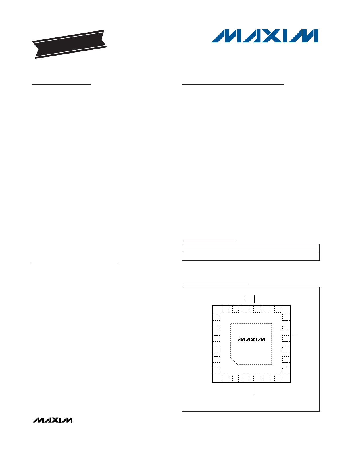
Pin Configuration
19-4209; Rev 0; 7/08
For pricing, delivery, and ordering information, please contact Maxim Direct at 1-888-629-4642,
or visit Maxim’s website at www.maxim-ic.com.
EVALUATION KIT
AVAILABLE
Functional Diagram and Typical Operating Circuit appear
at end of data sheet.
SPI and QSPI are trademarks of Motorola Inc.
MICROWIRE is a trademark of National Semiconductor Corp.
Ordering Information
+
Denotes a lead-free/RoHS-compliant package.
*
EP = Exposed pad.
PART TEMP RANGE PIN-PACKAGE
MAX5134AGTG+
24 TQFN-EP*
-40°C to +105°C
TOP VIEW
GND
N.C.
REF0
REFI
N.C.
AVDD
*EXPOSED PAD.
19
20
21
22
23
24
+
OUT1
12
OUT0
M/Z
N.C.
1718 16 14 13
N.C.
THIN QFN
4mm x 4mm
15
MAX5134
456
3
DVDD
LDAC
READY
N.C.
*EP
N.C.
OUT2
OUT3
12
SCLK
N.C.
11
CS
10
9
DIN
N.C.
8
GND
7
Page 2
MAX5134
Low-Power, Quad 16-Bit,
Buffered Voltage-Output DAC
2 _______________________________________________________________________________________
ABSOLUTE MAXIMUM RATINGS
ELECTRICAL CHARACTERISTICS
(V
AVDD
= 2.7V to 5.25V, V
DVDD
= 2.7V to 5.25V, V
AVDD
≥ V
DVDD
, V
GND
= 0, V
REFI
= V
AVDD
- 0.25V, C
OUT
= 200pF, R
OUT
= 10kΩ,
T
A
= T
MIN
to T
MAX
, unless otherwise noted. Typical values are at TA= +25°C.)
Stresses beyond those listed under “Absolute Maximum Ratings” may cause permanent damage to the device. These are stress ratings only, and functional
operation of the device at these or any other conditions beyond those indicated in the operational sections of the specifications is not implied. Exposure to
absolute maximum rating conditions for extended periods may affect device reliability.
AVDD to GND...........................................................-0.3V to +6V
DVDD to GND...........................................................-0.3V to +6V
OUT0–OUT3 to GND ....................................-0.3V to the lower of
(AVDD + 0.3V) and +6V
REFI, REFO, M/Z to GND .............................-0.3V to the lower of
(AVDD + 0.3V) and +6V
SCLK, DIN, CS to GND ................................-0.3V to the lower of
(DVDD + 0.3V) and +6V
LDAC, READY to GND .................................-0.3V to the lower of
(DVDD + 0.3V) and +6V
Continuous Power Dissipation (T
A
= +70°C)
24-Pin TQFN (derate at 17.5mW/°C above +70°C) 2222.2mW
Maximum Current into Any Input or Output
with the Exception of M/Z Pin .......................................±50mA
Maximum Current into M/Z Pin ...........................................±5mA
Operating Temperature Range .........................-40°C to +105°C
Storage Temperature Range .............................-65°C to +150°C
Lead Temperature (soldering, 10s) .................................+300°C
STATIC ACCURACY (Notes 1, 2)
Resolution N 16 Bits
Integral Nonlinearity INL
Differential Nonlinearity DNL Guaranteed monotonic -1.0 +1.0 LSB
Offset Error OE (Note 4) -10 ±1 +10 mV
Offset-Error Drift ±4 µV/°C
Gain Error GE (Note 4) -0.5 ±0.2 +0.5 % of FS
Gain Temperature Coefficient ±2
REFERENCE INPUT
Reference-Input Voltage Range V
Reference-Input Impedance 113 kΩ
INTERNAL REFERENCE
Reference Voltage V
Refer ence Tem p er atur e C oeffi ci ent (Note 5) 10 25 ppm/°C
Reference Output Impedance 1 Ω
Line Regulation 100 ppm/V
Maximum Capacitive Load C
PARAMETER SYMBOL CONDITIONS MIN TYP MAX UNITS
REFI
REFO
R
V
= 5V,
REFI
AVDD = 5.25V
AVDD = 3V to 5.25V 2 AVDD
AVDD = 2.7V to 3V 2
T
+25°C 2.434 2.440 2.443 V
A =
( N ote 3) -8 ±2 +10
= +25°C ±6
T
A
AVDD -
0.1 nF
0.2
LSB
ppm
FS/°C
V
Page 3
MAX5134
Low-Power, Quad 16-Bit,
Buffered Voltage-Output DAC
_______________________________________________________________________________________ 3
ELECTRICAL CHARACTERISTICS (continued)
(V
AVDD
= 2.7V to 5.25V, V
DVDD
= 2.7V to 5.25V, V
AVDD
≥ V
DVDD
, V
GND
= 0, V
REFI
= V
AVDD
- 0.25V, C
OUT
= 200pF, R
OUT
= 10kΩ,
T
A
= T
MIN
to T
MAX
, unless otherwise noted. Typical values are at TA= +25°C.)
DAC OUTPUT VOLTAGE (Note 2)
Output Voltage Range No load 0.02
DC Output Impedance 0.1 Ω
Maximum Capacitive Load
(Note 5)
Resistive Load R
Short-Circuit Current I
Power-Up Time From power-down mode 25 µs
DIGITAL INPUTS (SCLK, DIN, CS, LDAC) (Note 6)
Input High Voltage V
Input Low Voltage V
Input Leakage Current I
Input Capacitance C
DIGITAL OUTPUTS (READY)
Output High Voltage V
Output Low Voltage V
DYNAMIC PERFORMANCE
Voltage-Output Slew Rate SR Positive and negative 1.25 V/µs
Voltage-Output Settling Time t
Digital Feedthrough Code 0, all digital inputs from 0 to DVDD 0.5 nV•s
Major Code Transition Analog
Glitch Impulse
Output Noise 10kHz 120 nV/√Hz
Integrated Output Noise 1Hz to 10kHz 18 µV
DAC-to-DAC Crosstalk 25 nV•s
PARAMETER SYMBOL CONDITIONS MIN TYP MAX UNITS
C
SC
IN
OH
OL
Series resistance = 0 0.2 nF
L
Series resistance = 500Ω 15 µF
L
AVDD = 5.25V ±35
AVDD = 2.7V -40 ±20 +40
IH
IL
VIN = 0 or DVDD -1 ±0.1 +1 µA
IN
I
SOURCE
I
= 2mA 0.4 V
SINK
1/4 scale to 3/4 scale V
S
settle to ±2 LSB (Note 5)
= 3mA
= AVDD = 5V
REFI
2kΩ
0.7 x
DVDD
DVDD
- 0.5
5µs
12 nV•s
AVDD
- 0.02
0.3 x
DVDD
10 pF
V
mA
V
V
V
Page 4
MAX5134
Low-Power, Quad 16-Bit,
Buffered Voltage-Output DAC
4 _______________________________________________________________________________________
ELECTRICAL CHARACTERISTICS (continued)
(V
AVDD
= 2.7V to 5.25V, V
DVDD
= 2.7V to 5.25V, V
AVDD
≥ V
DVDD
, V
GND
= 0, V
REFI
= V
AVDD
- 0.25V, C
OUT
= 200pF, R
OUT
= 10kΩ,
T
A
= T
MIN
to T
MAX
, unless otherwise noted. Typical values are at TA= +25°C.)
Note 1: Static accuracy tested without load.
Note 2: Linearity is tested within 20mV of GND and AVDD
,
allowing for gain and offset error.
Note 3: Codes above 2047 are guaranteed to be within ±8 LSB
.
Note 4: Gain and offset tested within 100mV of GND and AVDD
.
Note 5: Guaranteed by design.
Note 6: Device draws current in excess of the specified supply current when a digital input is driven with a voltage of VI < DVDD - 0.6V
or VI > 0.5V. At VI = 2.2V with DVDD = 5.25V, this current can be as high as 2mA. The SPI inputs are CMOS-input level compatible. The 30MHz clock frequency cannot be guaranteed for a minimum signal swing.
Note 7: Excess current from AVDD is 10mA when powered without DVDD. Excess current from DVDD is 1mA when powered without
AVDD.
Note 8: All timing specifications are with respect to the digital input and output thresholds.
Note 9: Maximum daisy-chain clock frequency is limited to 25MHz.
C7
C6
C5 D2
D1
D0
X
COMMAND EXECUTED ON
24TH FALLING EDGE OF SCLK
CS
SCLK
DIN
X = DON'T CARE.
t
CH
t
CL
t
CSS
t
DH
t
CSH
t
DS
t
SRL
READY
X
t
CSW
D3
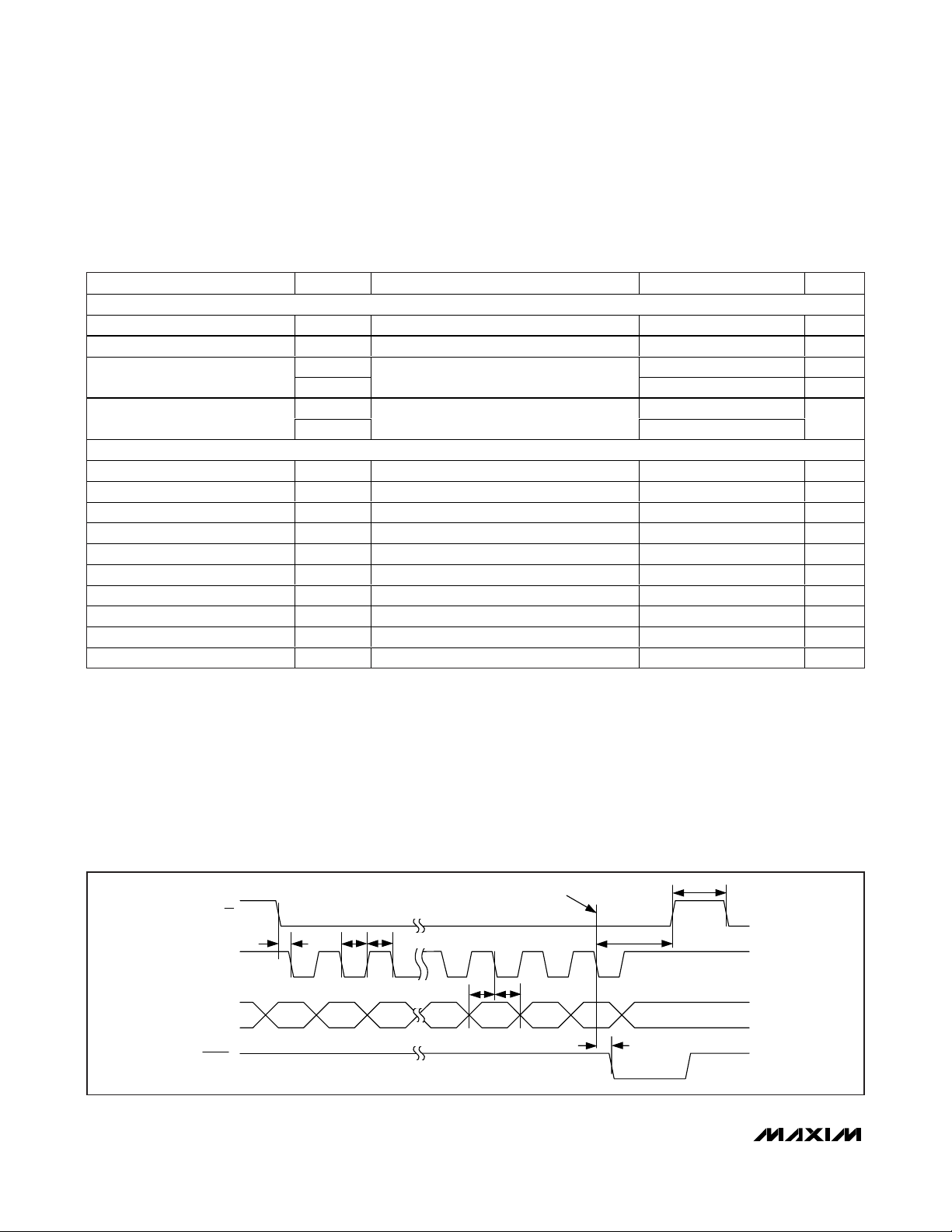
Figure 1. Serial-Interface Timing Diagram
PARAMETER SYMBOL CONDITIONS MIN TYP MAX UNITS
POWER REQUIREMENTS (Note 7)
Analog Supply Voltage Range AVDD 2.7 5.25 V
Digital Supply Voltage Range DVDD 2.7 AVDD V
Supply Current
Power-Down Supply Current
I
AVDD
I
DVDD
I
AVPD
I
DVPD
No load, all digital inputs at 0 or DVDD
No load, all digital inputs at 0 or DVDD
2.5 3.6 mA
110µA
0.2 2
0.1 2
TIMING CHARACTERISTICS (Note 8) (Figure 1)
Serial-Clock Frequency f
SCLK Pulse-Width High t
SCLK Pulse-Width Low t
CS Fall-to-SCLK Fall Setup Time t
SCLK Fall-to CS-Rise Hold Time t
DIN-to-SCLK Fall Setup Time t
DIN-to-SCLK Fall Hold Time t
SCLK Fall to READY Transition t
CS Pulse-Width High t
LDAC Pulse Width t
LDACPWL
SCLK
CH
CL
CSS
CSH
DS
DH
SRL
CSW
(Note 9) 30 ns
0 30 MHz
13 ns
13 ns
8ns
5ns
10 ns
2ns
33 ns
33 ns
µA
Page 5
MAX5134
Low-Power, Quad 16-Bit,
Buffered Voltage-Output DAC
_______________________________________________________________________________________ 5
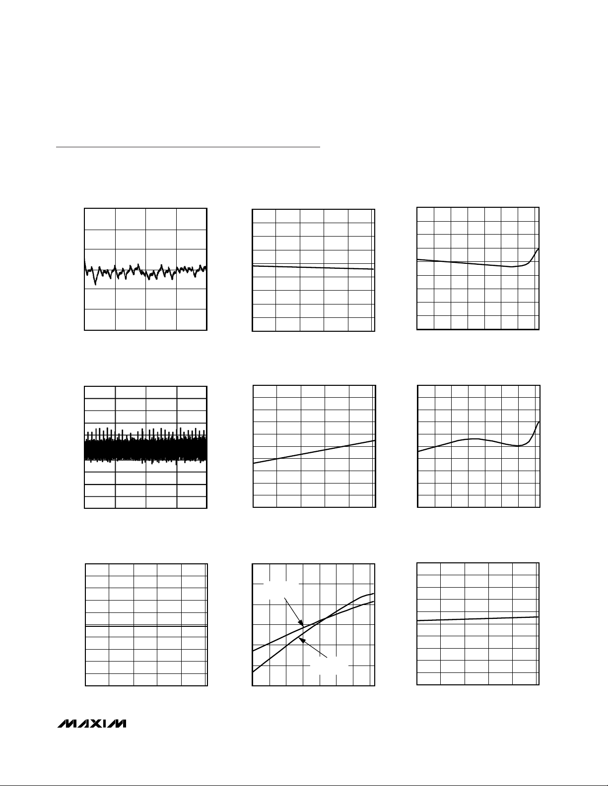
Typical Operating Characteristics
(TA = +25°C, unless otherwise noted.)
INTEGRAL NONLINEARITY
vs. DIGITAL OUTPUT CODE
9
6
3
0
INL (LSB)
-3
-6
-9
0 16384 32768
DIGITAL OUTPUT CODE (LSB)
49152 65536
DIFFERENTIAL NONLINEARITY
vs. DIGITAL OUTPUT CODE
1.0
0.8
0.6
0.4
0.2
0
DNL (LSB)
-0.2
-0.4
-0.6
-0.8
-1.0
16384 32768 49152 65536
0
DIGITAL OUTPUT CODE (LSB)
MAX5134 toc01
MAX5134 toc04
INTEGRAL NONLINEARITY
vs. ANALOG SUPPLY VOLTAGE
9
7
5
3
1
-1
INL (LSB)
-3
-5
-7
-9
2.7 3.7 4.73.2 4.2 5.2
AVDD ( V )
DIFFERENTIAL NONLINEARITY
vs. ANALOG SUPPLY VOLTAGE
1.0
0.8
0.6
0.4
0.2
0
DNL (LSB)
-0.2
-0.4
-0.6
-0.8
-1.0
2.7
3.2 4.2 5.2
3.7 4.7
AVDD ( V )
MAX5134 toc02
MAX5134 toc05
INTEGRAL NONLINEARITY
9
7
5
3
1
-1
INL (LSB)
-3
-5
-7
-9
-40 100-20 60 8040020
DIFFERENTIAL NONLINEARITY
1.0
0.8
0.6
0.4
0.2
0
DNL (LSB)
-0.2
-0.4
-0.6
-0.8
-1.0
-40
-20 0 20 40 60 80 100
vs. TEMPERATURE
MAX5134 toc03
TEMPERATURE (°C)
vs. TEMPERATURE
MAX5134 toc06
TEMPERATURE (°C)
OFFSET ERROR vs.
ANALOG SUPPLY VOLTAGE
10
8
6
4
2
0
-2
OFFSET ERROR (mV)
-4
-6
-8
-10
2.7 3.7 4.73.2 4.2 5.2
AVDD ( V )
-0.1
MAX5134 toc07
-0.2
-0.3
-0.4
OFFSET ERROR (mV)
-0.5
-0.6
OFFSET ERROR vs. TEMPERATURE
0
V
= 2.7V
AVDD
= 2.5V
V
REFI
V
= 5.25V
AVDD
= 5V
V
REFI
-40 20 80060-20 40 100
TEMPERATURE (°C)
0.5
0.4
MAX5134 toc08
0.3
0.2
0.1
-0.1
GAIN ERROR (%FS)
-0.2
-0.3
-0.4
-0.5
GAIN ERROR vs.
ANALOG SUPPLY VOLTAGE
MAX5134 toc09
0
2.7 3.7 4.73.2 4.2 5.2
AVDD ( V )
Page 6
MAX5134
Low-Power, Quad 16-Bit,
Buffered Voltage-Output DAC
6 _______________________________________________________________________________________
Typical Operating Characteristics (continued)
(TA = +25°C, unless otherwise noted.)
GAIN ERROR vs. TEMPERATURE
MAX5134 toc10
TEMPERATURE (°C)
GAIN ERROR (%FS)
-40 20 80060-20 40 100
0.070
0.080
0.076
0.082
0.078
0.072
0.074
0.084
0.086
V
AVDD
= 2.7V
V
AVDD
= 5.25V
SUPPLY CURRENT
vs. TEMPERATURE
MAX5134 toc11
TEMPERATURE (°C)
SUPPLY CURRENT (μA)
100806040200-20
500
1000
1500
2000
2500
0
-40
I
AVDD
I
DVDD
ANALOG SUPPLY CURRENT
vs. ANALOG SUPPLY VOLTAGE
MAX5134 toc12
SUPPLY VOLTAGE (V)
4.74.23.73.2
1600
1700
1800
1900
2000
2100
2200
2300
2400
2500
1500
2.7 5.2
V
OUT
= 0
V
OUT
= V
REFO
V
DVDD
= 2.7V
EXITING/ENTERING
POWER-DOWN MODE
MAX5134 toc14
4μs/div
CH1
CH0
500mV/div
500mV/div
MAJOR CODE TRANSITION
MAX5134 toc15
1μs/div
10mV/div
SETTLING TIME UP
MAX5134 toc16
400ns/div
500mV/div
SETTLING TIME DOWN
MAX5134 toc17
400ns/div
500mV/div
CROSSTALK
MAX5134 toc18
4μs/div
10mV/div
2V/div
SUPPLY CURRENT vs. SUPPLY VOLTAGE
0.50
0.45
0.40
0.35
0.30
0.25
0.20
0.15
SUPPLY CURRENT (µA)
0.10
0.05
0
(POWER-DOWN MODE)
TA = -40°C
TA = +105°C
TA = +25°C
2.7 5.2
SUPPLY VOLTAGE (V)
4.74.23.73.2
MAX5134 toc13
Page 7

MAX5134
Low-Power, Quad 16-Bit,
Buffered Voltage-Output DAC
_______________________________________________________________________________________ 7
)
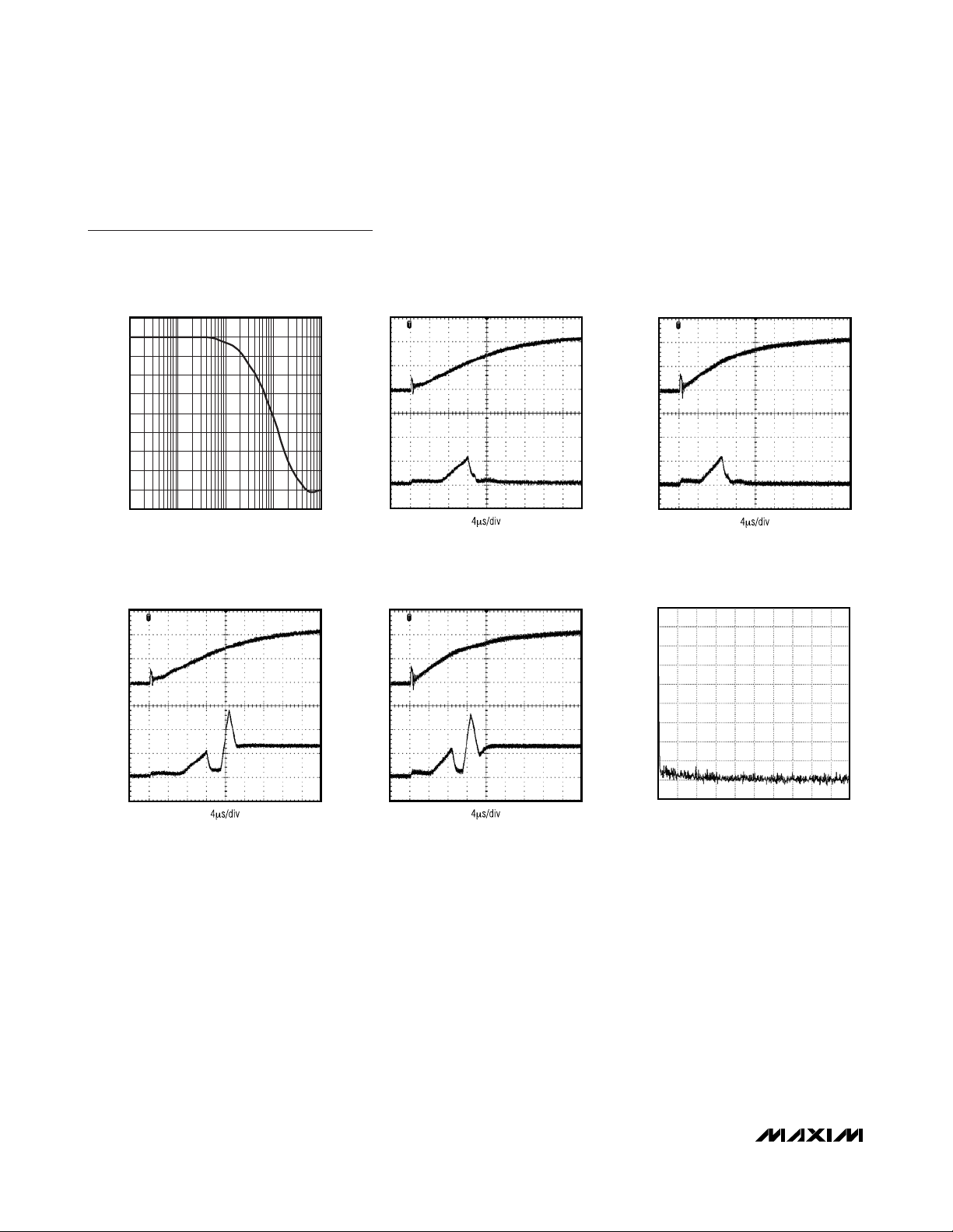
Typical Operating Characteristics (continued)
(TA = +25°C, unless otherwise noted.)
DIGITAL FEEDTHROUGH
SCLK
V
OUT
40ns/div
REFERENCE VOLTAGE
vs. TEMPERATURE
2.4405
2.4400
2.4395
2.4390
(V)
REFO
V
2.4385
2.4380
2.4375
2.4370
-40
TEMPERATURE (°C)
MAX5134 toc19
100806040200-20
5V/div
50mV/div
MAX5134 toc22
DIGITAL SUPPLY CURRENT vs.
DIGITAL SUPPLY VOLTAGE
4.0
V
= 5.25V
AVDD
3.5
3.0
2.5
2.0
1.5
SUPPLY CURRENT (nA)
1.0
0.5
0
2.7 5.2
SUPPLY VOLTAGE (V)
DIGITAL SUPPLY CURRENT
vs. DIGITAL INPUT VOLTAGE
3000
V
= V
= 5.25V
DVDD
UP
DOWN
DIGITAL INPUT VOLTAGE (V)
DIGITAL SUPPLY CURRENT (µA)
2500
2000
1500
1000
500
AVDD
0
0
2.50
MAX5134 toc20
4.74.23.73.2
MAX5134 toc23
54321
2.48
2.46
(V)
REFO
V
2.44
2.42
2.40
2.51
2.50
2.49
2.48
2.47
2.46
OUTPUT VOLTAGE (V)
2.45
2.44
2.43
REFERENCE VOLTAGE vs.
SUPPLY VOLTAGE
TA = +25°C
TA = -40°C
2.7 5.2
SUPPLY VOLTAGE (V)
TA = +105°C
4.74.23.73.2
FULL-SCALE OUTPUT
vs. TEMPERATURE
EXTERNAL
REFERENCE
2.500V
INTERNAL
REFERENCE
-40
TEMPERATURE (°C)
MAX5134 toc21
MAX5134 toc24
10080-20 0 20 40 60
OUTPUT VOLTAGE
2.50
2.45
2.40
2.35
2.30
2.25
2.20
OUTPUT VOLTAGE (V)
2.15
2.10
2.05
2.00
030
V
= 3.3V
AVDD
OUTPUT CURRENT (mA
V
= 5V
AVDD
MAX5134 toc25
252015105
vs. OUTPUT CURRENT
FULL-SCALE REFERENCE FEEDTHROUGH
V
OUT
REF
MAX5134 toc26
500mV/div
500mV/div
0V V
OUT
0V V
REF
ZERO-SCALE REFERENCE FEEDTHROUGH
V
REF
V
OUT
20μs/div
MAX5134 toc27
500mV/div
10mV/div
Page 8
MAX5134
Low-Power, Quad 16-Bit,
Buffered Voltage-Output DAC
8 _______________________________________________________________________________________
Typical Operating Characteristics (continued)
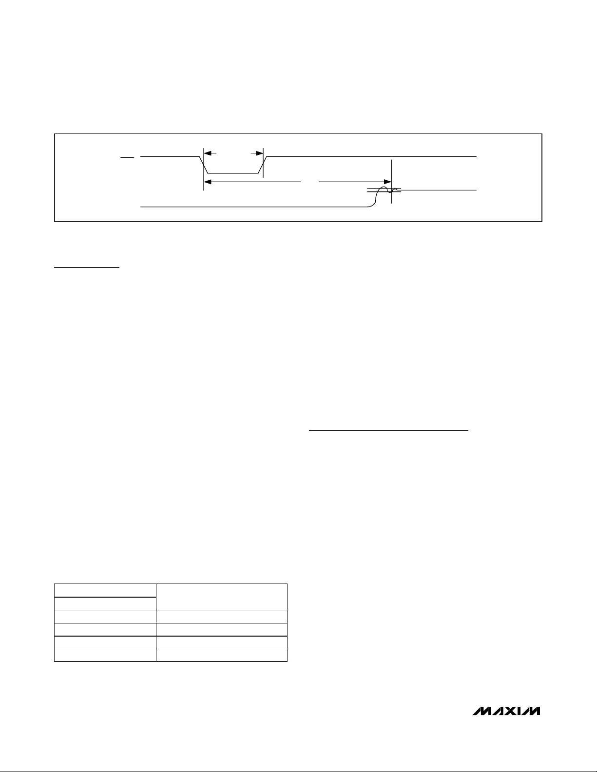
(TA = +25°C, unless otherwise noted.)
REFERENCE INPUT BANDWIDTH
vs. FREQUENCY
5
0
-5
-10
-15
-20
-25
ATTENUATION (dB)
-30
-35
-40
-45
1
INPUT FREQUENCY (kHz)
POWER-UP GLITCH, MIDSCALE,
EXTERNAL REFERENCE
V
AVDD
MAX5134 toc31
10,000100010010
MAX5134 toc28
2V/div
V
V
POWER-UP GLITCH, ZERO SCALE,
EXTERNAL REFERENCE
AVDD
V
OUT
POWER-UP GLITCH, MIDSCALE,
INTERNAL REFERENCE
AVDD
MAX5134 toc29
MAX5134 toc32
2V/div
1V/div
2V/div
V
POWER-UP GLITCH, ZERO SCALE,
INTERNAL REFERENCE
AVDD
V
OUT
DC NOISE SPECTRUM, FFT PLOT
MAX5134 toc30
MAX5134 toc33
2V/div
1V/div
-40dBm
10dB/div
1V/div
V
V
OUT
OUT
1V/div
2.5kHz/div 25kHz
Page 9

Detailed Description
The MAX5134 low-power, quad 16-bit, digital-to-analog
converter (DAC) uses a precision internal reference or
an external reference for rail-to-rail operation to provide
high-linearity buffered voltage outputs. The MAX5134
minimizes the digital noise feedthrough from input to output by powering down the SCLK and DIN input buffers
after completion of each 24-bit serial input. On powerup, the MAX5134 resets the DAC outputs to zero or midscale, depending on the state of the M/Z input, providing
additional safety for applications that drive valves or
other transducers that need to be off on power-up. The
MAX5134 contains a segmented resistor string-type
DAC, a serial-in parallel-out shift register, a DAC register, power-on reset (POR) circuit, and control logic. On
the falling edge of the clock (SCLK) pulse, the serial
input (DIN) data is shifted into the device, MSB first.
During power-down, an internal 80kΩ resistor pulls DAC
outputs to GND.
Output Amplifiers (OUT0–OUT3)
The MAX5134 includes internal buffers for all DAC outputs. The internal buffers provide improved load regulation and transition glitch suppression for the DAC
outputs. The output buffers slew at 1.25V/µs and drive up
to 2kΩ in parallel with 200pF. The analog supply voltage
(AVDD) determines the maximum output voltage range
of the device as AVDD powers the output buffers.
DAC Reference
Internal Reference
The MAX5134 features an internal reference with a
nominal output of +2.44V. Connect REFO to REFI when
using the internal reference. Bypass REFO to GND with
a 47pF (maximum 100pF) capacitor. Alternatively if
heavier decoupling is required, use a 1kΩ series resistor with a 1µF capacitor to ground. REFO can deliver up
to 100µA of current with no degradation in performance. Configure other reference voltages by applying
a resistive potential divider with a total resistance
greater than 33kΩ from REFO to GND.
MAX5134
Low-Power, Quad 16-Bit,
Buffered Voltage-Output DAC
_______________________________________________________________________________________ 9
Pin Description
PIN NAME FUNCTION
1 OUT0 Channel 0 Buffered DAC Output
2, 5, 8, 11,
14, 17, 20,
23
3 DVDD Digital Power Supply. Bypass DVDD with a 0.1µF capacitor to GND.
4 READY
6 OUT3 Channel 3 Buffered DAC Output
7, 19 GND Ground
9 DIN Data In
10 CS Active-Low Chip-Select Input
12 SCLK Seria-Clock Input
13 OUT2 Channel 2 Buffered DAC Output
15 LDAC Load DAC Input. Active-low hardware load DAC input.
16 M/Z
18 OUT1 Channel 1 Buffered DAC Output
21 REFO Reference Voltage Output
22 REFI Reference Voltage Input. Bypass REFI with a 0.1µF capacitor to GND when using external reference.
24 AVDD Analog Power Supply. Bypass AVDD with a 0.1µF capacitor to GND.
—EP
N.C. No Connection. Not internally connected.
Active-Low Ready. Indicated configuration ready. Use READY as CS for consecutive part or as feedback
to the µC.
Power-Up Reset Select. Connect M/Z to DVDD to power up the DAC outputs to midscale. Connect M/Z
to GND to power up the DAC outputs to zero.
Exposed Pad. Internally connected to GND. Connect to a large ground plane to maximize thermal
performance. Not intended as an electrical connection point.
Page 10

MAX5134
External Reference
The external reference input features a typical input
impedance of 113kΩ and accepts an input voltage
from +2V to AVDD. Connect an external voltage
supply between REFI and GND to apply an external reference. Leave REFO unconnected. Visit
www.maxim-ic.com/products/references for a list of
available external voltage-reference devices.
AVDD as Reference
Connect AVDD to REFI to use AVDD as the reference
voltage. Leave REFO unconnected.
Serial Interface
The MAX5134 3-wire serial interface is compatible with
MICROWIRE, SPI, QSPI, and DSPs (Figures 2, 3). The
interface provides three inputs, SCLK, CS, and DIN and
one output, READY. Use READY to verify communication or to daisy-chain multiple devices (see the
READY
section). READY is capable of driving a 20pF load with
a 30ns (max) delay from the falling edge of SCLK. The
chip-select input (CS) frames the serial data loading at
DIN. Following a chip-select input’s high-to-low transi-
tion, the data is shifted synchronously and latched into
the input register on each falling edge of the serialclock input (SCLK). Each serial word is 24 bits. The first
8 bits are the control word followed by 16 data bits
(MSB first), as shown in Table 1. The serial input register transfers its contents to the input registers after
loading 24 bits of data. To initiate a new data transfer,
drive CS high, keep CS high for a minimum of 33ns
before the next write sequence. The SCLK can be
either high or low between CS write pulses. Figure 1
shows the timing diagram for the complete 3-wire serialinterface transmission.
The MAX5134 digital inputs are double buffered.
Depending on the command issued through the serial
interface, the input register(s) can be loaded without
effecting the DAC register(s) using the write command.
To update the DAC registers, either pulse the LDAC input
low to asynchronously update all DAC outputs, or use the
software LDAC command. Use the write through commands (see Table 1) to update the DAC outputs immediately after the data is received. Only use the write through
command to update the DAC output immediately.
Low-Power, Quad 16-Bit,
Buffered Voltage-Output DAC
10 ______________________________________________________________________________________
Table 1. Operating Mode Truth Table
24-BIT WORD
CONTROL BITS DATA BITS
MSB LSB
C7 C6 C5 C4 C3 C2 C1 C0 D15 D14 D13 D12 D11 D10 D9 D8 D7 D6–D0
0 0 0 0 0 0 0 0 X X X X X X X X X X NOP No operation.
0 0 0 0 0 0 0 1 XXXX
0 0 0 0 0 0 1 0 X X X X X X X X X X CLR Software clear.
0 0 0 0 0 0 1 1 XXXX
0 0 0 0 0 1 0 1 0 0 0 0 0 0 LIN 0 0 0 Linearity Optimize DAC linearity.
0 0 0 1
0 0 1 1
0 0 1 0 0 0 0 0 X X X X X X X X X X NOP No operation.
DAC3DAC2DAC1DAC
0
DAC3DAC2DAC1DAC
0
D15 D14 D13 D12 D11 D10 D9 D8 D7 D6 Write
D15 D14 D13 D12 D11 D10 D9 D8 D7 D6
DAC3DAC2DAC1DAC
0
DAC3DAC2DAC1DAC
0
X X LDAC
READY_EN X
DESC FUNCTION
Move contents of input
to DAC registers
indicated by 1’s. No
effect on registers
indicated by 0’s.
Power down DAC’s
Power
Control
Write
Through
indicated by 1’s.
Set READY_EN = 1 to
enable READY.
Write to selected input
registers (DAC output
not affected).
Write to selected input
and DAC registers, DAC
outputs updated (write
through).
Page 11

MAX5134
Low-Power, Quad 16-Bit,
Buffered Voltage-Output DAC
______________________________________________________________________________________ 11
Figure 2. Connections for MICROWIRE
The 16-bit DAC code is unipolar binary with V
OUT
=
(code/65536) x V
REF
. See Table 1 for the serial inter-
face commands
Connect the MAX5134 DVDD supply to the supply of
the host DSP or microprocessor. The AVDD supply may
be set to any voltage within the operating range of 2.7V
to 5.25V, but must be greater than or equal to the
DVDD supply.
Writing to the MAX5134
Write to the MAX5134 using the following sequence:
1) Drive CS low, enabling the shift register.
2) Clock 24 bits of data into DIN (C7 first and D0 last),
observing the specified setup and hold times. Bits
D15–D0 are the data bits that are written to the
internal register.
3) After clocking in the last data bit, drive CS high. CS
must remain high for 33ns before the next transmission is started.
Figure 1 shows a write operation for the transmission of
24 bits. If CS is driven high at any point prior to receiving
24 bits, the transmission is discarded.
READY
Connect READY to a microcontroller (µC) input to monitor the serial interface for valid communications. The
READY pulse appears 24 clock cycles after the negative edge of CS (Figure 4). Since the MAX5134 looks at
the first 24 bits of the transmission following the falling
edge of CS, it is possible to daisy chain devices with
different command word lengths. READY goes high
16ns after CS is driven high.
READY*
DIN
SCLK
CS
SCK
SS
I/O
MOSI
+5V
MISO*
SPI/QSPI
PORT
*THE READY-TO-MISO CONNECTION IS NOT REQUIRED FOR WRITING TO THE
MAX5134 BUT MAY BE USED FOR TRANSMISSION VERIFICATION.
MAX5134
Figure 3. Connections for SPI/QSPI
CS
DIN
SCLK
READY 1
READY 3
READY 2
12324222120432 1 23 2422215432 1 23 2422215432
SLAVE 1 DATA SLAVE 2 DATA SLAVE 3 DATA
Figure 4. READY Timing
SK
SO
MICROWIRE
PORT
MAX5134
SCLK
DIN
READY*
CS
*THE READY-TO-SI CONNECTION IS NOT REQUIRED FOR WRITING TO THE MAX5134
*BUT MAY BE USED FOR TRANSMISSION VERIFICATION.
SI*
I/O
Page 12

MAX5134
Daisy chain multiple MAX5134 devices by connecting
the first device conventionally, then connect its READY
output to the CS of the following device. Repeat for any
other devices in the chain, and drive the SCLK and DIN
lines in parallel (Figure 5). When sending commands to
daisy-chained MAX5134s, the devices are accessed
serially starting with the first device in the chain. The first
24 data bits are read by the first device, the second 24
data bits are read by the second device and so on
(Figure 4). Figure 6 shows the configuration when CS is
not driven by the µC.
To perform a daisy-chain write operation, drive CS low
and output the data serially to DIN. The propagation of
the READY signal then controls how the data is read by
each device. As the data propagates through the daisy
chain, each individual command in the chain is executed on the 24th falling clock edge following the falling
edge of the respective CS input. To update just one
device in a daisy chain, send the no-op command to
the other devices in the chain.
If READY is not required, write command 0x03 (power
control) and set READY_EN = 0 (see Table 1) to disable the READY output.
Clear Command
The MAX5134 features a software clear command
(0x02). The software clear command acts as a software
POR, erasing the contents of all registers. All outputs
return to the state determined by the M/Z input.
Power-Down Mode
The MAX5134 features a software-controlled individual
power-down mode for each channel. The internal reference and biasing circuits power down to conserve
power when all 4 channels are powered down. In
power-down, the outputs disconnect from the buffers
and are grounded with an internal 80kΩ resistor. The
DAC register holds the retained code so that the output
is restored when the channel powers up. The serial
interface remains active in power-down mode.
Load DAC (
LDAC
) Input
The MAX5134 features an active-low LDAC logic input
that allows the outputs to update asynchronously. Keep
LDAC high during normal operation (when the device is
controlled only through the serial interface). Drive LDAC
low to simultaneously update all DAC outputs with data
from their respective input registers. Figure 7 shows the
LDAC timing with respect to OUT_. Holding LDAC low
causes the input registers to become transparent and
data written to the DAC registers to immediately update
the DAC outputs. A software command can also activate the LDAC operation. To activate LDAC by software,
set control word 0x01 and data bits A11–A8 to select
which DAC to load, and all other data bits to don’t care.
See Table 1 for the data format. This operation updates
only the DAC outputs that are flagged with a “1”.
DAC outputs flagged with a “0” remain unchanged.
Low-Power, Quad 16-Bit,
Buffered Voltage-Output DAC
12 ______________________________________________________________________________________
Figure 5. Daisy-Chain Configuration
μC
MOSI
SCK
SLAVE 1
DIN
SCLK
I/O
READY
CS
DIN
SCLK
CS
SLAVE 2
READY
DIN
SCLK
CS
SLAVE 3
READY
Page 13

MAX5134
Low-Power, Quad 16-Bit,
Buffered Voltage-Output DAC
______________________________________________________________________________________ 13
μC
Figure 6. Daisy Chain (CS Not Used)
CSm
CS1
SCLK
DWRITE
DREAD
INT
TO OTHER CHIPS/CHAINS
SLAVE 1
CS
CS
SCLK
DIN
READY
SLAVE 2
CS
SCLK
DIN
READY
SLAVE N
CS
SCLK
DIN
DOUT
ERROR
READY
Page 14
MAX5134
Applications Information
Power-On Reset (POR)
On power-up, the input registers are set to zero, DAC
outputs power up to zero or midscale, depending on
the configuration of M/Z. Connect M/Z to GND to power
the outputs to GND. Connect M/Z to AVDD to power the
outputs to midscale.
To optimize DAC linearity, wait until the supplies have
settled. Set the LIN bit in the DAC linearity register; wait
10ms, and clear the LIN bit.
Unipolar Output
The MAX5134 unipolar output voltage range is 0 to
V
REFI
. The output buffers each drive a load of 2kΩ in
parallel with 200pF.
Bipolar Output
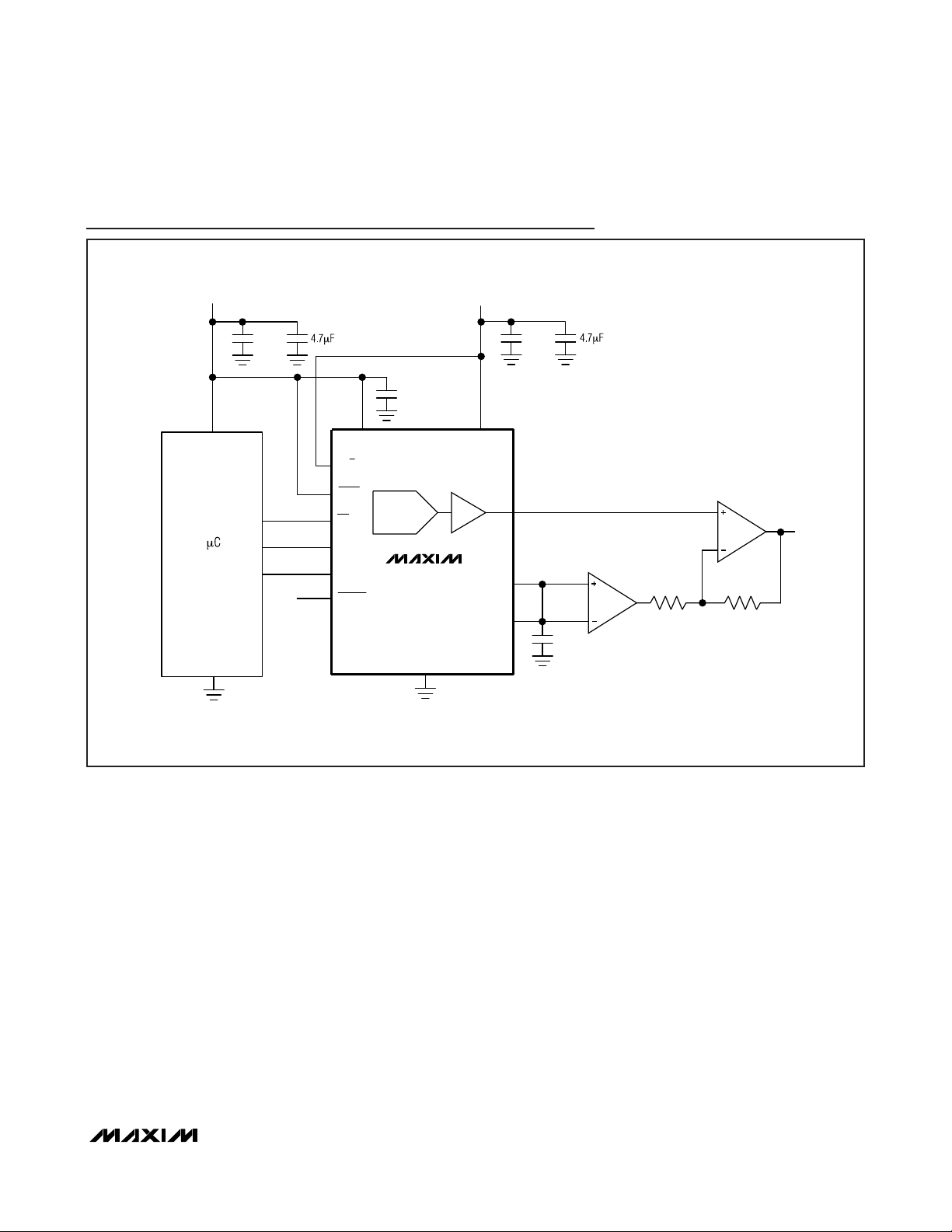
Use the MAX5134 in bipolar applications with additional
external components (see the
Typical Operating Circuit
).
Power Supplies and
Bypassing Considerations
For best performance, use a separate supply for the
MAX5134. Bypass both DVDD and AVDD with highquality ceramic capacitors to a low-impedance ground
as close as possible to the device. Minimize lead
lengths to reduce lead inductance. Connect both
MAX5134 GND inputs to the analog ground plane.
Layout Considerations
Digital and AC transient signals on GND inputs can create noise at the outputs. Connect both GND inputs to
form the star ground for the DAC system. Refer remote
DAC loads to this system ground for the best possible
performance. Use proper grounding techniques, such
as a multilayer board with a low-inductance ground
plane, or star connect all ground return paths back to
the MAX5134 GND. Carefully lay out the traces
between channels to reduce AC crosscoupling and
crosstalk. Do not use wire-wrapped boards and sockets. Use shielding to improve noise immunity. Do not
run analog and digital signals parallel to one another
(especially clock signals) and avoid routing digital lines
underneath the MAX5134 package.
Definitions
Integral Nonlinearity (INL)
INL is the deviation of the measured transfer function
from a best fit straight line drawn between two codes.
This best fit line is a line drawn between codes 3072
and 64,512 of the transfer function, once offset and
gain errors have been nullified.
Differential Nonlinearity (DNL)
DNL is the difference between an actual step height
and the ideal value of 1 LSB. If the magnitude of the
DNL is greater than -1 LSB, the DAC guarantees no
missing codes and is monotonic.
Offset Error
Offset error indicates how well the actual transfer function matches the ideal transfer function at a single point.
Typically, the point at which the offset error is specified is
at or near the zero-scale point of the transfer function.
Low-Power, Quad 16-Bit,
Buffered Voltage-Output DAC
14 ______________________________________________________________________________________
Figure 7. Output Timing
Table 2. Input Code vs. Output Voltage
t
LDAC
LDACPWL
OUT_
t
S
±2 LSB
DAC LATCH CONTENTS
MSB LSB
1111 1111 1111 1111 V
1000 0000 0000 0000 V
0000 0000 0000 0001 V
0000 0000 0000 0000 0
ANALOG OUTPUT, V
x (65,535/65,536)
REF
x (32,768/65,536) = 1/2 V
REF
x (1/65,536)
REF
OUT
REF
Page 15

Gain Error
Gain error is the difference between the ideal and the
actual full-scale output voltage on the transfer curve,
after nullifying the offset error. This error alters the slope
of the transfer function and corresponds to the same
percentage error in each step.
Settling Time
The settling time is the amount of time required from the
start of a transition, until the DAC output settles to the new
output value within the converter’s specified accuracy.
Digital Feedthrough
Digital feedthrough is the amount of noise that appears
on the DAC output when the DAC digital control lines
are toggled.
Digital-to-Analog Glitch Impulse
A major carry transition occurs at the midscale point
where the MSB changes from low to high and all other
bits change from high to low, or where the MSB
changes from high to low and all other bits change from
low to high. The duration of the magnitude of the
switching glitch during a major carry transition is
referred to as the digital-to-analog glitch impulse.
Digital-to-Analog Power-Up Glitch Impulse
The digital-to-analog power-up glitch is the duration of
the magnitude of the switching glitch that occurs as the
device exits power-down mode.
DC DAC-to-DAC Crosstalk
Crosstalk is the amount of noise that appears on a DAC
output set to 0 when the other DAC is updated from 0 to
AVDD
Chip Information
PROCESS: BiCMOS
MAX5134
Low-Power, Quad 16-Bit,
Buffered Voltage-Output DAC
______________________________________________________________________________________ 15
Page 16

MAX5134
Low-Power, Quad 16-Bit,
Buffered Voltage-Output DAC
16 ______________________________________________________________________________________
Functional Diagram
M/Z
CS
SCLK
DIN
MAX5134
SERIAL-TO-
PARALLEL
CONVERTER
POR
CONTROL LOGIC
INPUT
REGISTER
INPUT
REGISTER
INPUT
REGISTER
INPUT
REGISTER
AVDD DVDD
POWER-DOWN
CONTROL
DAC
REGISTER
DAC
REGISTER
DAC
REGISTER
DAC
REGISTER
GND
16-BIT
DAC
16-BIT
DAC
16-BIT
DAC
16-BIT
DAC
REFI
REFO
REFERENCE
BUFFER
BUFFER
BUFFER
BUFFER
OUT0
OUT1
OUT2
OUT3
READY
LDAC
Page 17
MAX5134
Low-Power, Quad 16-Bit,
Buffered Voltage-Output DAC
______________________________________________________________________________________ 17
Typical Operating Circuit
DIGITAL POWER
SUPPLY
100nF
ANALOG POWER
100nF
DVDD AVDD
M/Z
LDAC
CS
SCLK
DIN
READY
DAC
MAX5134
GND
SUPPLY
OUT
REFO
REFI
100nF
R1
47pF
R2
*SHOWN IN BIPOLAR CONFIGURATION
Page 18
MAX5134
Low-Power, Quad 16-Bit,
Buffered Voltage-Output DAC
Maxim cannot assume responsibility for use of any circuitry other than circuitry entirely embodied in a Maxim product. No circuit patent licenses are
implied. Maxim reserves the right to change the circuitry and specifications without notice at any time.
18
____________________Maxim Integrated Products, 120 San Gabriel Drive, Sunnyvale, CA 94086 408-737-7600
© 2008 Maxim Integrated Products is a registered trademark of Maxim Integrated Products, Inc.
PACKAGE TYPE PACKAGE CODE DOCUMENT NO.
24 TQFN T2444-4
21-0139
Package Information
For the latest package outline information and land patterns, go to www.maxim-ic.com/packages.
 Loading...