

General Description
The MAX5128 nonvolatile, single, linear-taper, digital
potentiometer performs the function of a mechanical
potentiometer, but replaces the mechanics with a simple 2-wire digital interface. The MAX5128 performs the
same function as a discrete potentiometer or variable
resistor and features 128 taps and 22kΩ end-to-end
resistance. The MAX5128 also features an ultra-small,
2mm x 2mm µDFN package and low 0.5µA (typ) standby supply current, making this device ideal for portable
applications. The MAX5128 operates from a +2.7V to
+5.25V power supply. An integrated nonvolatile memory recalls the programmed wiper position of the digital
potentiometer. A simple 2-wire up/down interface programs the wiper position. The digital potentiometer provides a low 5ppm/°C ratiometric temperature coefficient
and is specified over the extended -40°C to +85°C temperature range.
Applications
V
COM
Adjustment for LCD Panels
Backlight Adjustment
LED Bias Adjustment
Power-Supply Modules
Fiber-Module Bias Setting
Bias Setting for Radios
Portable Consumer Electronics
Features
♦ Ultra-Small, 2mm x 2mm, 8-Pin µDFN Package
♦ Power-On Recall of Wiper Position from
Nonvolatile Memory
♦ 22kΩ End-to-End Resistance
♦ 128 Tap Positions
♦ 5ppm/°C Ratiometric Temperature Coefficient
♦ 1.5µA (max) Standby Supply Current
♦ +2.7V to +5.25V Single Supply Operation
♦ 80,000 Wiper Store Cycles
♦ 50-Year Wiper Data Retention
MAX5128
128-Tap, Nonvolatile, Linear-Taper Digital
Potentiometer in 2mm x 2mm µDFN Package
________________________________________________________________ Maxim Integrated Products 1
19-3929; Rev 2; 6/07
For pricing, delivery, and ordering information, please contact Maxim/Dallas Direct! at
1-888-629-4642, or visit Maxim’s website at www.maxim-ic.com.
EVALUATION KIT
AVAILABLE
Ordering Information
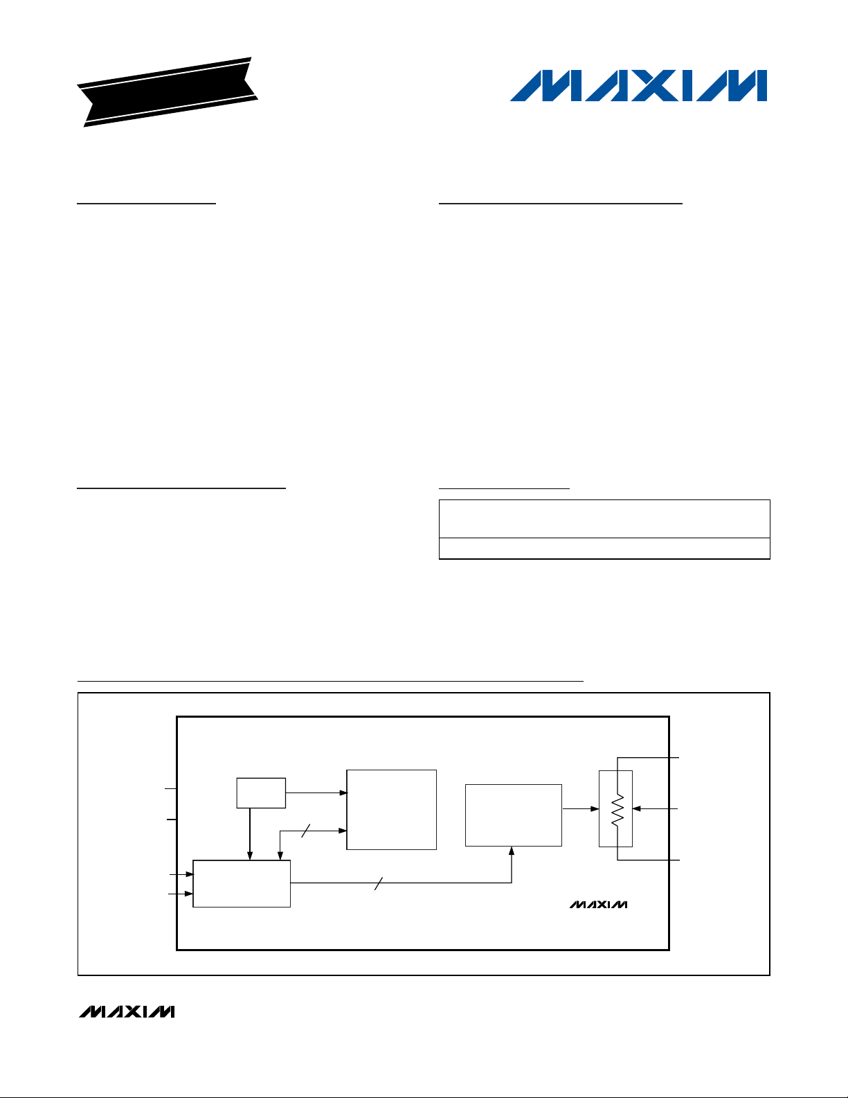
Functional Diagram
+Denotes a lead-free package.
PART
M AX 5128E LA+ -40°C to +85°C 8 µDFN AAF L822-1
TEMP
RANGE
PIN PA C K A G E
TOP
MARK
PKG
CODE
H
V
CC
GND
UP
DN
SERIAL
INTERFACE
POR
7
7-BIT NV MEMORY
7
128-POSITION
DECODER
128
TAPS
MAX5128
W
L
MAX5128
128-Tap, Nonvolatile, Linear-Taper Digital
Potentiometer in 2mm x 2mm µDFN Package
2 _______________________________________________________________________________________
ABSOLUTE MAXIMUM RATINGS
Stresses beyond those listed under “Absolute Maximum Ratings” may cause permanent damage to the device. These are stress ratings only, and functional
operation of the device at these or any other conditions beyond those indicated in the operational sections of the specifications is not implied. Exposure to
absolute maximum rating conditions for extended periods may affect device reliability.
VCCto GND...........................................................-0.3V to +6.0V
UP and DN to GND ....................................-0.3V to (V
CC
+ 0.3V)
H, L, and W to GND....................................-0.3V to (V
CC
+ 0.3V)
Maximum Continuous Current into H, L, and W ..............±0.5mA
Maximum Continuous Current into All Other Pins ............±50mA
Continuous Power Dissipation (T
A
= +70°C)
8-Pin µDFN (derate 4.7mW/°C above +70°C) ........376.5mW
Operating Temperature Range ...........................-40°C to +85°C
Junction Temperature......................................................+150°C
Storage Temperature Range .............................-60°C to +150°C
Lead Temperature (soldering, 10s) .................................+300°C
ELECTRICAL CHARACTERISTICS
(VCC= +2.7V to +5.25V, H = VCC, L = GND, TA= -40°C to +85°C. Typical values are at VCC= +5.0V, TA= +25°C, unless otherwise noted.)
(Note 1)
DC PERFORMANCE (voltage-divider mode)
Resolution N 7 Bits
Integral Nonlinearity INL (Note 2) ±1.0 LSB
Differential Nonlinearity DNL (Note 2) ±1.0 LSB
End-to-End Resistance
Temperature Coefficient
Ratiometric Resistance
Temperature Coefficient
Full-Scale Error FSE -3 0 LSB
Zero-Scale Error ZSE 0 +2 LSB
DC PERFORMANCE (variable-resistor mode)
Integral Nonlinearity INL (Note 3) ±1.75 LSB
Differential Nonlinearity DNL (Note 3) ±1 LSB
DC PERFORMANCE (resistor characteristics)
Wiper Resistance R
Wiper Capacitance C
End-to-End Resistance R
DIGITAL INPUTS (UP, DN)
Input-High Voltage (Note 5) V
Input-Low Voltage V
Input Leakage Current I
Input Capacitance C
DYNAMIC CHARACTERISTICS
Wiper -3dB Bandwidth f
THD Plus Noise THD+N
PARAMETER SYMBOL CONDITIONS MIN TYP MAX UNITS
TC
R
(Note 4) 0.6 0.8 kΩ
W
W
HL
3.4V ≤ VCC ≤ 5.25V 2.4
IH
2.7V ≤ VCC < 3.4V
(Note 5)
IL
IN
IN
3dB
(Note 6) 400 kHz
V
= 0.3V
H
midscale
RMS
50 ppm/°C
5 ppm/°C
20 pF
16 22 27 kΩ
0.7 x
V
CC
0.8
±1 µA
5pF
, f = 1kHz, wiper set to
0.02 %
V
V
MAX5128
128-Tap, Nonvolatile, Linear-Taper Digital
Potentiometer in 2mm x 2mm µDFN Package
_______________________________________________________________________________________ 3
ELECTRICAL CHARACTERISTICS (continued)
(VCC= +2.7V to +5.25V, H = VCC, L = GND, TA= -40°C to +85°C. Typical values are at VCC= +5.0V, TA= +25°C, unless otherwise noted.)
(Note 1)
TIMING CHARACTERISTICS
(VCC= +2.7V to +5.25V, H = VCC, L = GND, TA= -40°C to +85°C. Typical values are at VCC= +5.0V, TA= +25°C, unless otherwise noted.)
(See Figures 1, 2, 3, and 4).
NONVOLATILE MEMORY RELIABILITY
Data Retention TA = +85°C 50 Years
Endurance
POWER SUPPLY
Supply Voltage V
Average Programming Current I
Peak Programming Current I
Standby Current I
PARAMETER SYMBOL CONDITIONS MIN TYP MAX UNITS
CC
PG
PK
CC
TA = +25°C 80,000
= +85°C 50,000
T
A
2.70 5.25 V
During nonvolatile write only;
digital inputs = V
During nonvolatile write only;
digital inputs = V
Digital inputs = VCC or GND, TA = +25°C 0.5 1.5 µA
or GND
CC
or GND
CC
220 400 µA
4mA
Stores
PARAMETER SYMBOL CONDITIONS MIN TYP MAX UNITS
ANALOG SECTION
Wiper Settling Time t
DIGITAL SECTION
UP or DN Pulse-Width High t
UP or DN Pulse-Width Low t
UP or DN Glitch Immunity t
UP Fall to DN Rise Setup or DN
Fall to UP Rise Setup
Before Entering NVM-Write
Mode, UP Fall to UP Rise
UP Rise to DN Rise Setup when
Entering NVM-Write
PWH
PWL
IMMU
t
MS1
t
MS2
t
WS
(Note 7) 500 ns
S
80 ns
80 ns
20 ns
80 ns
80 ns
80 ns
UP Fall to DN Fall Hold or DN Fall
to UP Fall Hold during NVMWrite
t
WH
0ns
MAX5128
128-Tap, Nonvolatile, Linear-Taper Digital
Potentiometer in 2mm x 2mm µDFN Package
4 _______________________________________________________________________________________
TIMING CHARACTERISTICS (continued)
(VCC= +2.7V to +5.25V, H = VCC, L = GND, TA= -40°C to +85°C. Typical values are at VCC= +5.0V, TA= +25°C, unless otherwise noted.)
(See Figures 1, 2, 3, and 4).
Note 1: All devices are production tested at TA= +25°C and are guaranteed by design for TA= -40°C to +85°C.
Note 2: The DNL and INL are measured with the potentiometer configured as a voltage-divider with H = V
CC
and L = GND. The
wiper terminal is unloaded and measured with a high input-impedance voltmeter.
Note 3: The DNL and INL are measured with the potentiometer configured as a variable resistor. H is unconnected and L = GND.
For the +5V condition, the wiper terminal is driven with a source current of 200µA and for the +2.7V condition, the wiper terminal is driven with a source current of 100µA.
Note 4: The wiper resistance is measured using the source currents given in Note 3.
Note 5: The device draws higher supply current when the digital inputs are driven with voltages between (V
CC
- 0.5V) and (GND +
0.5V). See Supply Current vs. Digital Input Voltage in the Typical Operating Characteristics.
Note 6: Wiper at midscale with a 10pF load, L = GND, an AC source is applied to H, and the output is measured as 3dB lower than
the DC W/H value in dB.
Note 7: Wiper-settling time is the worst-case 0 to 50% rise time measured between consecutive wiper positions. H = V
CC
, L = GND,
and the wiper terminal is unloaded and measured with a 10pF oscilloscope probe. See the Tap-to-Tap Switching Transient
in the Typical Operating Characteristics section.
Note 8: Power-up settling time is measured from the time V
CC
= 2.7V to the wiper settling to 1 LSB of the final value.
PARAMETER SYMBOL CONDITIONS MIN TYP MAX UNITS
NVM-Write Mode Pulse-Width
High
Write NV Register Busy Time t
Power-Up Settling Time t
t
WP
BUSY
ACC
80 ns
14 ms
(Note 8) 2 µs
MAX5128
128-Tap, Nonvolatile, Linear-Taper Digital
Potentiometer in 2mm x 2mm µDFN Package
_______________________________________________________________________________________ 5
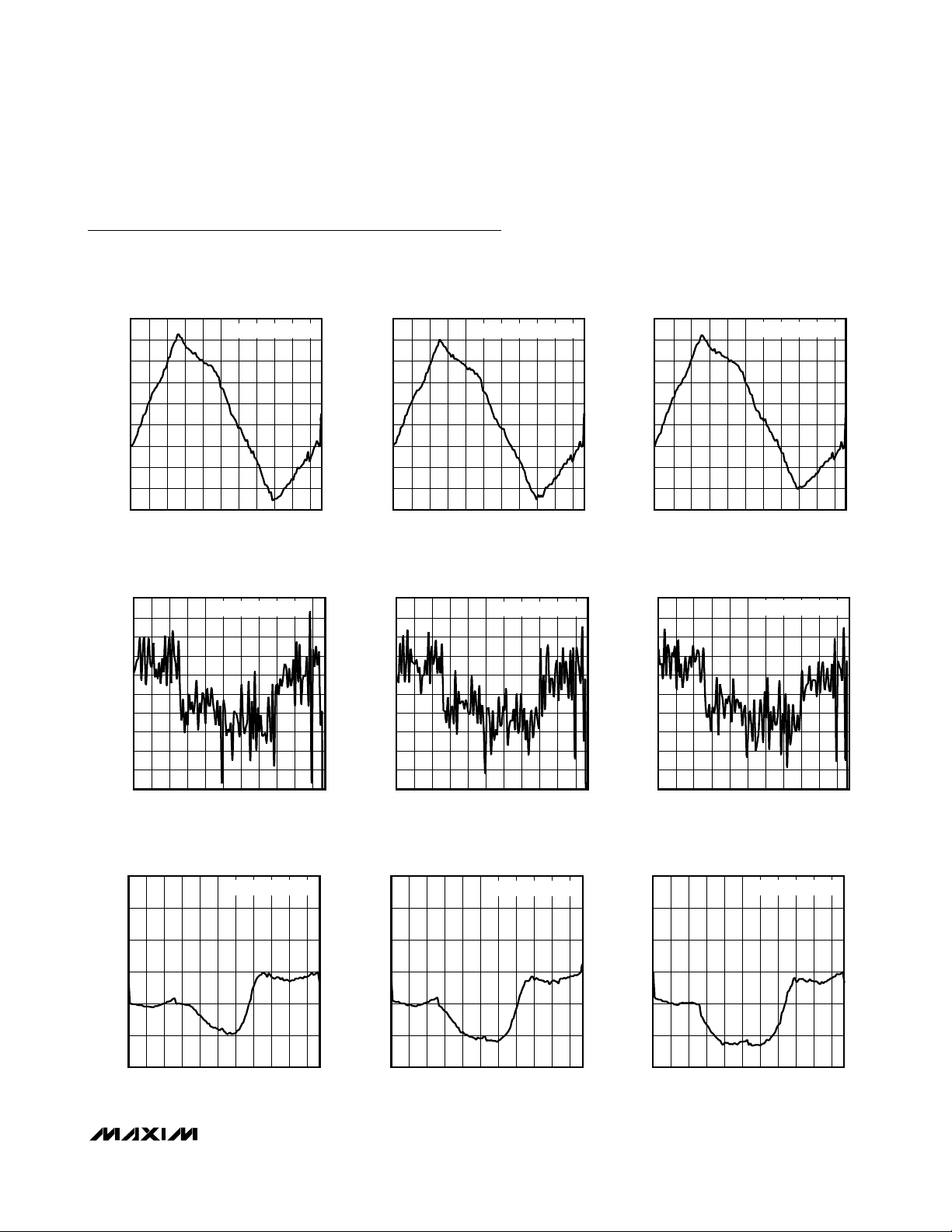
Typical Operating Characteristics
(VCC= +5.0V, TA= +25°C, unless otherwise noted.)
INTEGRAL NONLINEARITY
vs. CODE (VOLTAGE-DIVIDER)
0.12
0.10
0.08
0.06
0.04
0.02
INL (LSB)
0
-0.02
-0.04
-0.06
0243612 48 60 72 84 96 108 120
VCC = 2.7V, TA = -40°C
CODE
MAX5128 toc01
0.12
0.10
0.08
0.06
0.04
0.02
INL (LSB)
-0.02
-0.04
-0.06
DIFFERENTIAL NONLINEARITY
vs. CODE (VOLTAGE-DIVIDER)
MAX5128 toc04
0.010
0.008
0.006
0.004
0.002
DNL (LSB)
-0.002
-0.004
-0.006
-0.008
-0.010
0.010
0.008
0.006
0.004
0.002
0
DNL (LSB)
-0.002
-0.004
-0.006
-0.008
-0.010
0243612 48 60 72 84 96 108 120
VCC = 2.7V, TA = -40°C
CODE
INTEGRAL NONLINEARITY
vs. CODE (VOLTAGE-DIVIDER)
VCC = 2.7V, TA = +25°C
0
0243612 48 60 72 84 96 108 120
CODE
DIFFERENTIAL NONLINEARITY
vs. CODE (VOLTAGE-DIVIDER)
VCC = 2.7V, TA = +25°C
0
0243612 48 60 72 84 96 108 120
CODE
MAX5128 toc02
MAX5128 toc05
INTEGRAL NONLINEARITY
vs. CODE (VOLTAGE-DIVIDER)
0.12
0.10
0.08
0.06
0.04
0.02
INL (LSB)
0
-0.02
-0.04
-0.06
0243612 48 60 72 84 96 108 120
VCC = 2.7V, TA = +85°C
CODE
DIFFERENTIAL NONLINEARITY
vs. CODE (VOLTAGE-DIVIDER)
0.010
0.008
0.006
0.004
0.002
0
DNL (LSB)
-0.002
-0.004
-0.006
-0.008
-0.010
0243612 48 60 72 84 96 108 120
VCC = 2.7V, TA = +85°C
CODE
MAX5128 toc03
MAX5128 toc06
INTEGRAL NONLINEARITY
vs. CODE (VARIABLE RESISTOR)
1.5
1.0
0.5
0
INL (LSB)
-0.5
-1.0
-1.5
0243612 48 60 72 84 96 108 120
VCC = 2.7V, TA = -40°C
CODE
MAX5128 toc07
INTEGRAL NONLINEARITY
vs. CODE (VARIABLE RESISTOR)
1.5
1.0
0.5
0
INL (LSB)
-0.5
-1.0
-1.5
0243612 48 60 72 84 96 108 120
VCC = 2.7V, TA = +25°C
CODE
MAX5128 toc08
INTEGRAL NONLINEARITY
vs. CODE (VARIABLE RESISTOR)
1.5
1.0
0.5
0
INL (LSB)
-0.5
-1.0
-1.5
0243612 48 60 72 84 96 108 120
VCC = 2.7V, TA = +85°C
CODE
MAX5128 toc09
MAX5128
128-Tap, Nonvolatile, Linear-Taper Digital
Potentiometer in 2mm x 2mm µDFN Package
6 _______________________________________________________________________________________
Typical Operating Characteristics (continued)
(VCC= +5.0V, TA= +25°C, unless otherwise noted.)
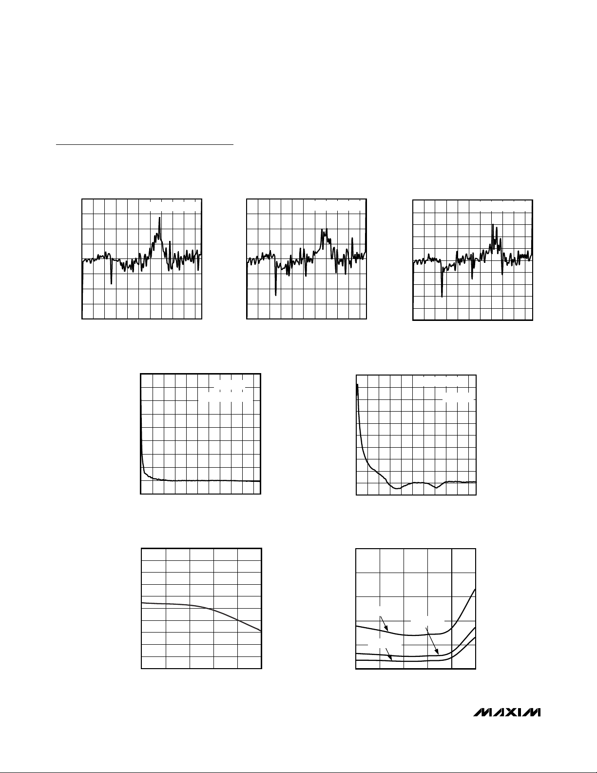
DIFFERENTIAL NONLINEARITY
vs. CODE (VARIABLE RESISTOR)
0.20
0.15
0.10
0.05
0
DNL (LSB)
-0.05
-0.10
-0.15
-0.20
0243612 48 60 72 84 96 108 120
160
140
120
100
RATIOMETRIC TEMPCO (ppm/°C)
MAX5128 toc10
0.20
0.15
0.10
0.05
0
DNL (LSB)
-0.05
-0.10
-0.15
-0.20
0243612 48 60 72 84 96 108 120
VCC = 2.7V, TA = -40°C
CODE
RATIOMETRIC TEMPERATURE
COEFFICIENT vs. CODE (VOLTAGE-DIVIDER)
VCC = 2.7V
TA = -40°C TO +85°C
80
60
40
20
0
-20
0243612 48 60 72 84 96 108 120
CODE
DIFFERENTIAL NONLINEARITY
vs. CODE (VARIABLE RESISTOR)
VCC = 2.7V, TA = +25°C
CODE
900
MAX5128 toc13
800
700
600
500
400
(ppm/°C)
VR
300
TC
200
100
0
-100
DIFFERENTIAL NONLINEARITY
vs. CODE (VARIABLE RESISTOR)
0.25
0.20
MAX5128 toc11
0.15
0.10
0.05
0
DNL (LSB)
-0.05
-0.10
-0.15
-0.20
-0.25
0243612 48 60 72 84 96 108 120
TEMPERATURE COEFFICIENT
vs. CODE (VARIABLE RESISTOR)
TA = -40°C TO +85°C
VCC = 2.7V
0243612 48 60 72 84 96 108 120
CODE
VCC = 2.7V, TA = +85°C
MAX5128 toc12
CODE
MAX5128 toc14
END-TO-END RESISTANCE (RHL)
% CHANGE vs. TEMPERATURE
1.0
0.8
0.6
0.4
0.2
0
-0.2
-0.4
-0.6
END-TO-END RESISTANCE CHANGE (%)
-0.8
-1.0
-40 10-15 35 60 85
TEMPERATURE (°C)
MAX5128 toc15
1.5
1.2
0.9
(μA)
DD
I
0.6
0.3
STANDBY SUPPLY CURRENT
vs. TEMPERATURE
VCC = 5.25V
VCC = 3.3V
VCC = 2.7V
0
-40 10-15 35 60 85
TEMPERATURE (°C)
MAX5128 toc16

MAX5128
128-Tap, Nonvolatile, Linear-Taper Digital
Potentiometer in 2mm x 2mm µDFN Package
_______________________________________________________________________________________ 7
Typical Operating Characteristics (continued)
(VCC= +5.0V, TA= +25°C, unless otherwise noted.)
SUPPLY CURRENT
vs. DIGITAL INPUT VOLTAGE
1000
100
(μA)
10
DD
I
1
0.1
0 5.0
DIGITAL INPUT VOLTAGE (V)
10
VCC = 5V
WIPER = MIDSCALE
FILTER BANDWIDTH = 80kHz
1
VCC = 5V
4.54.03.53.02.52.01.51.00.5
THD+N vs. FREQUENCY
MAX5128 toc17
1000
(Ω)
W
R
800
600
400
200
0
WIPER RESISTANCE
vs. TEMPERATURE
VCC = 5V
WIPER = MIDSCALE
-40 10-15 35 60 85
TEMPERATURE (°C)
TAP-TO-TAP SWITCHING TRANSIENT
MAX5128 toc20
MAX5128 toc18
WIPER RESPONSE
vs. FREQUENCY
0
-2
-4
-6
-8
-10
GAIN (dB)
-12
-14
-16
-18
0.1 1 10 100 1000
FREQUENCY (kHz)
MAX5128 toc21
VCC = 5V
WIPER = MIDSCALE
UP
2V/div
MAX5128 toc19
0.1
THD+N (%)
0.01
0.001
0.0001
0.1 100
FREQUENCY (kHz)
101
WIPER RESISTANCE vs. CODE
600
500
400
(Ω)
300
W
R
200
100
0
0243612 48 60 72 84 96 108 120
CODE
MAX5128 toc22
H = V
CC
L = GND
FROM MIDSCALE
= 20pF
C
W
1μs/div
MIDSCALE WIPER TRANSIENT
AT POWER-ON
10μs/div
MAX5128 toc23
V
W
20mV/div
AC-COUPLED
V
CC
2V/div
OUTPUT
W
2V/div

MAX5128
Detailed Description
The MAX5128 nonvolatile, single, linear-taper, digital
potentiometer performs the function of a mechanical
potentiometer or variable resistor, but replaces the
mechanics with a simple 2-wire digital interface. This
device features 128 taps and 22kΩ end-to-end resistance with a 5ppm/°C ratiometric temperature coefficient. The MAX5128 operates from a +2.7V to +5.25V
power supply and consumes only 0.5µA (typ) of standby supply current. The MAX5128 includes an integrated nonvolatile memory that recalls the stored wiper
position of the digital potentiometer. A simple 2-wire
up/down interface programs the wiper positions.
Analog Circuitry
The MAX5128 consists of a resistor array with 127
resistive elements; 128 tap points along the resistor
string between H and L are accessible to the wiper, W.
Select the wiper tap point by programming the potentiometer through the 2-wire (UP, DN) interface.
The MAX5128 features power-on reset circuitry that
loads the wiper position from the nonvolatile memory at
power-up.
The nonvolatile memory is programmed to midscale at
the factory.
128-Tap, Nonvolatile, Linear-Taper Digital
Potentiometer in 2mm x 2mm µDFN Package
8 _______________________________________________________________________________________
Pin Description
Figure 1. Digital-Interface Timing Diagram
PIN NAME FUNCTION
1V
2H
3 W Wiper Terminal
4L
5 GND Ground
6 DN Down Input
7 UP Up Input
8 N.C. No Connection. Not internally connected.
CC
Power Supply. Bypass VCC with a 0.1µF capacitor to GND as close to the device as possible. For proper
operation, limit the supply voltage slew rate to ≥ 10µs.
High Terminal. The voltage at H can be higher than or lower than the voltage at L. Current can flow into or
out of H.
Low Terminal. The voltage at L can be higher than or lower than the voltage at H. Current can flow into or out
of L.
t
PWH
t
PWL
UP
DN
t
MS1
NVM WRITE
t
MS1
t
PWL
t
PWH
t
WP
t
WS
t
WH
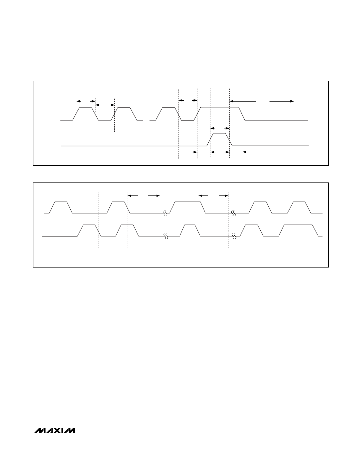
Digital Interface
The MAX5128 features a 2-wire interface consisting of
two logic inputs (UP and DN). Logic inputs UP and DN
control the wiper position and program the position to
the nonvolatile memory. Transition UP from high to low
with DN low to increment the wiper position. Transition
DN from high to low with UP low to decrement the wiper
position (see Figures 1, 2, and 3). When the wiper decrements, it decreases the resistance between W and L
(and it increases the resistance between H and W).
To program the nonvolatile memory, force UP high,
then force DN high, and then transition either input
(UP/DN) from high to low (see Figure 3).
The wiper performs a make-before-break transition,
ensuring that an open circuit during a transition from
one resistor tap to another does not occur. The wiper
does not wrap around when it reaches either end of the
resistor array (max/min). Additional transition com-
mands in the direction of the end point do not change
the tap position.
The logic inputs also feature pulse glitch immunity
(20ns) to protect the wiper from transitioning due to
glitches (see Figure 4).
Write NV Register
The internal EEPROM consists of a 7-bit nonvolatile
memory that retains the value written to it even after
power-down. To program the nonvolatile memory, force
UP high, then force DN high, and then transition either
input (UP/DN) from high to low. A nonvolatile write
requires a busy time of 14ms (max). During the busy
time, any nonvolatile write requests are ignored as well
as requests to increment or decrement the wiper position. Upon power-up, the wiper returns to the position
stored in the nonvolatile register. The MAX5128 features a factory-default wiper position of midscale.
MAX5128
128-Tap, Nonvolatile, Linear-Taper Digital
Potentiometer in 2mm x 2mm µDFN Package
_______________________________________________________________________________________ 9
Figure 2. Digital-Interface Timing Diagram with t
BUSY
Figure 3. Digital-Interface Command Diagram
NVM
t
PWH
UP
t
PWL
t
MS2
WRITE
t
WP
t
BUSY
DN
UP
DN
WIPER
INCREMENTS
WIPER
DECREMENTS
NVM
WRITE
t
BUSY
NVM
WRITE
t
WS
t
BUSY
t
WH
WIPER
INCREMENTS
WIPER
DECREMENTS

MAX5128
Standby Mode
The MAX5128 operates in standby mode while the serial interface is inactive. Programming the MAX5128
increases the average operating current to 400µA
(max). When in standby mode, the static supply current
reduces to less than 0.5µA (typ).
Power-Up
Upon power-up, the MAX5128 updates the wiper position with the data stored in the nonvolatile memory. This
initialization period takes 2µs (typ). For proper operation, limit the supply voltage slew rate to ≥ 10µs.
Applications Information
Use the MAX5128 for applications requiring digitally
controlled adjustable resistance or voltage, such as
LCD contrast control (where voltage biasing adjusts the
display contrast), or DC-DC converters with adjustable
outputs. The 22kΩ end-to-end resistance is divided into
128 tap points of 172Ω each. Use the MAX5128 in a
voltage-divider or variable-resistor configuration.
V
COM
Generator
Figure 5 shows an application using the MAX4238 and
the MAX5128 to generate the V
COM
voltage for a LCD
panel. Adjusting the resistor value of the MAX5128
changes the V
COM
voltage. Adjusting the V
COM
volt-
age changes the contrast for the LCD panel.
DC-DC Converter Applications
Figures 6 and 7 show two applications using the
MAX5128 to adjust the output voltage of a DC-DC converter. Figure 6 shows the MAX5128 in the grounded
potentiometer configuration. Figure 7 shows the
MAX5128 in a floating potentiometer configuration. The
grounded potentiometer configuration forces the output
voltage range of the DC-DC converter to fall within the
supply voltage range of the MAX5128. Use the floating
potentiometer configuration to allow the DC-DC converter’s output to exceed the supply voltage range of
the MAX5128. The floating potentiometer configuration
increases the output voltage range and increases the
precision of the output voltage adjustment range.
LED Bias Adjustment
Figure 8 shows a LED bias adjustment application
using a MAX5128 to set the current of the LEDs that the
MAX1574 drives. Use the MAX5128 for an adjustable
LED current drive of 10mA to 60mA.
Chip Information
PROCESS: BiCMOS
128-Tap, Nonvolatile, Linear-Taper Digital
Potentiometer in 2mm x 2mm µDFN Package
10 ______________________________________________________________________________________
Figure 4. Glitch-Immunity Timing Diagram
t
IMMU
t
IMMU
UP
DN
PULSES WITH WIDTHS LESS THAN t
ARE IGNORED.
IMMU
t
IMMU
t
IMMU

MAX5128
128-Tap, Nonvolatile, Linear-Taper Digital
Potentiometer in 2mm x 2mm µDFN Package
______________________________________________________________________________________ 11
Figure 5. V
COM
Generator Circuit for LCD Panels
Figure 6. DC-DC Converter Using a Grounded Potentiometer
= 0.8V
V
IN
TO V
OUT
TIMING-CONTROL-IC
OUTPUT SIGNAL
LX
MAX1722
BATT
GND
OUT
FB
10kΩ
+3.3V
W
27kΩ
36kΩ
MAX5128
0.1μF
H
L
V
= 2V
OUT
TO 5.25V
15kΩ
MAX4238
+5V
0.1μF
+3.3V
120kΩ
H
W
L
22kΩ
51kΩ
MAX5128
V
COM

MAX5128
128-Tap, Nonvolatile, Linear-Taper Digital
Potentiometer in 2mm x 2mm µDFN Package
12 ______________________________________________________________________________________
Figure 7. DC-DC Converter Using a Floating Potentiometer
Figure 8. LED Bias Adjustment Using the MAX5128
123
87465
N.C. DN GNDUP
V
CC
LWH
MAX5128
TOP VIEW
2mm x 2mm μDFN
Pin Configuration
SW
V
= 2.7V TO 5.5V
CC
V
CC
SHDN
CPCN
VIN = 2.7V
TO 5.5V
IN
MAX1574
H
OUT
LED1
MAX8574
GND
V
LX
H
FB
W
MAX5128
L
= VCC TO 28V
OUT
MAX5128
W
SET
L
GND
LED2
LED3

MAX5128
128-Tap, Nonvolatile, Linear-Taper Digital
Potentiometer in 2mm x 2mm µDFN Package
______________________________________________________________________________________ 13
Package Information
(The package drawing(s) in this data sheet may not reflect the most current specifications. For the latest package outline information,
go to www.maxim-ic.com/packages
.)
D
XXXX
XXXX
XXXX
PIN 1
INDEX AREA
SAMPLE
MARKING
7
A
E
L
e
C
L
A A
(N/2 -1) x e)
b
N
SOLDER
MASK
COVERAGE
PIN 1
0.10x45∞
1
L1
C
L
6, 8, 10L UDFN.EPS
-DRAWING NOT TO SCALE-
A1
b
A
A2
L
e
EVEN TERMINAL
e
ODD TERMINAL
PACKAGE OUTLINE,
6, 8, 10L uDFN, 2x2x0.80 mm
21-0164
L
1
A
2

MAX5128
128-Tap, Nonvolatile, Linear-Taper Digital
Potentiometer in 2mm x 2mm µDFN Package
Maxim cannot assume responsibility for use of any circuitry other than circuitry entirely embodied in a Maxim product. No circuit patent licenses are
implied. Maxim reserves the right to change the circuitry and specifications without notice at any time.
14 ____________________Maxim Integrated Products, 120 San Gabriel Drive, Sunnyvale, CA 94086 408-737-7600
© 2007 Maxim Integrated Products is a registered trademark of Maxim Integrated Products, Inc.
Boblet
Package Information (continued)
(The package drawing(s) in this data sheet may not reflect the most current specifications. For the latest package outline information,
go to www.maxim-ic.com/packages
.)
Revision History
Pages changed at Rev 1: 1, 9, 10, 13
Pages changed at Rev 2: 1, 9–14
COMMON DIMENSIONS
SYMBOL MIN. NOM.
A
A1
A2
D 1.95 2.00
E
L
L1
PACKAGE VARIATIONS
PKG. CODE N e b
0.70 0.75
0.15 0.20 0.25
0.020 0.025 0.035
1.95 2.00
0.30 0.40
MAX.
0.80
2.05
-
2.05
0.50
0.10 REF.
6L622-1 0.65 BSC 0.30±0.05
0.25±0.050.50 BSC8L822-1
0.20±0.030.40 BSC10L1022-1
(N/2 -1) x e
1.30 REF.
1.50 REF.
1.60 REF.
PACKAGE OUTLINE,
-DRAWING NOT TO SCALE-
6, 8, 10L uDFN, 2x2x0.80 mm
21-0164
2
A
2
 Loading...