For free samples & the latest literature: http://www.maxim-ic.com, or phone 1-800-998-8800.
For small orders, phone 1-800-835-8769.
General Description
The MAX5120/MAX5121 are low-power, 12-bit, voltageoutput digital-to-analog converters (DACs) with an internal precision bandgap reference and an output amplifier.
The MAX5120 operates on a +5V supply with an internal
amplifier reference of +2.5V and is capable of a +4.095V
full-scale output range. The MAX5121, operating on +3V,
delivers its +2.0475V full-scale output with an internal
precision reference of +1.25V. If necessary, the user can
override the internal, <10ppm/°C voltage reference with
an external reference. Both devices draw only 500µA of
supply current, which reduces to 3µA in power-down
mode. In addition, their power-up reset feature allows for
a user-selectable initial output state of either 0V or midscale and minimizes output voltage glitches during
power-up.
The serial interface is compatible with SPI™, QSPI™
and MICROWIRE™, which makes the MAX5120/
MAX5121 suitable for cascading multiple devices. Each
DAC has a double-buffered input organized as an input
register followed by a DAC register. A 16-bit shift register loads data into the input register. The DAC register
may be updated independently or simultaneously with
the input register.
Both devices are available in a 16-pin QSOP package
and are specified for the extended industrial (-40°C to
+85°C) temperature range. For pin-compatible 14-bit
upgrades, see the MAX5170/MAX5172 data sheet;
for pin-compatible 13-bit versions, see the MAX5130/
MAX5131 data sheet.
________________________Applications
Industrial Process Controls
Automatic Test Equipment (ATE)
Digital Offset and Gain Adjustment
Motion Control
µP-Controlled Systems
Features
♦ Single-Supply Operation
+5V (MAX5120)
+3V (MAX5121)
♦ Full-Scale Output Range
+4.095V (MAX5120)
+2.0475V (MAX5121)
♦ Built-In 10ppm/°C (max) Precision Bandgap
Reference
+2.5V (MAX5120)
+1.25V (MAX5121)
♦ Adjustable Output Offset
♦ SPI/QSPI/MICROWIRE-Compatible, 3-Wire Serial
Interface
♦ Pin-Programmable Shutdown Mode and Power-
Up Reset (0V or Midscale Output Voltage)
♦ Buffered Output Capable of Driving 5kΩ 100pF
or 4–20mA Loads
♦ Space-Saving 16-Pin QSOP Package
♦ Pin-Compatible 13-Bit Upgrades Available
(MAX5130/MAX5131)
♦ Pin-Compatible 14-Bit Upgrades Available
(MAX5170/MAX5172)
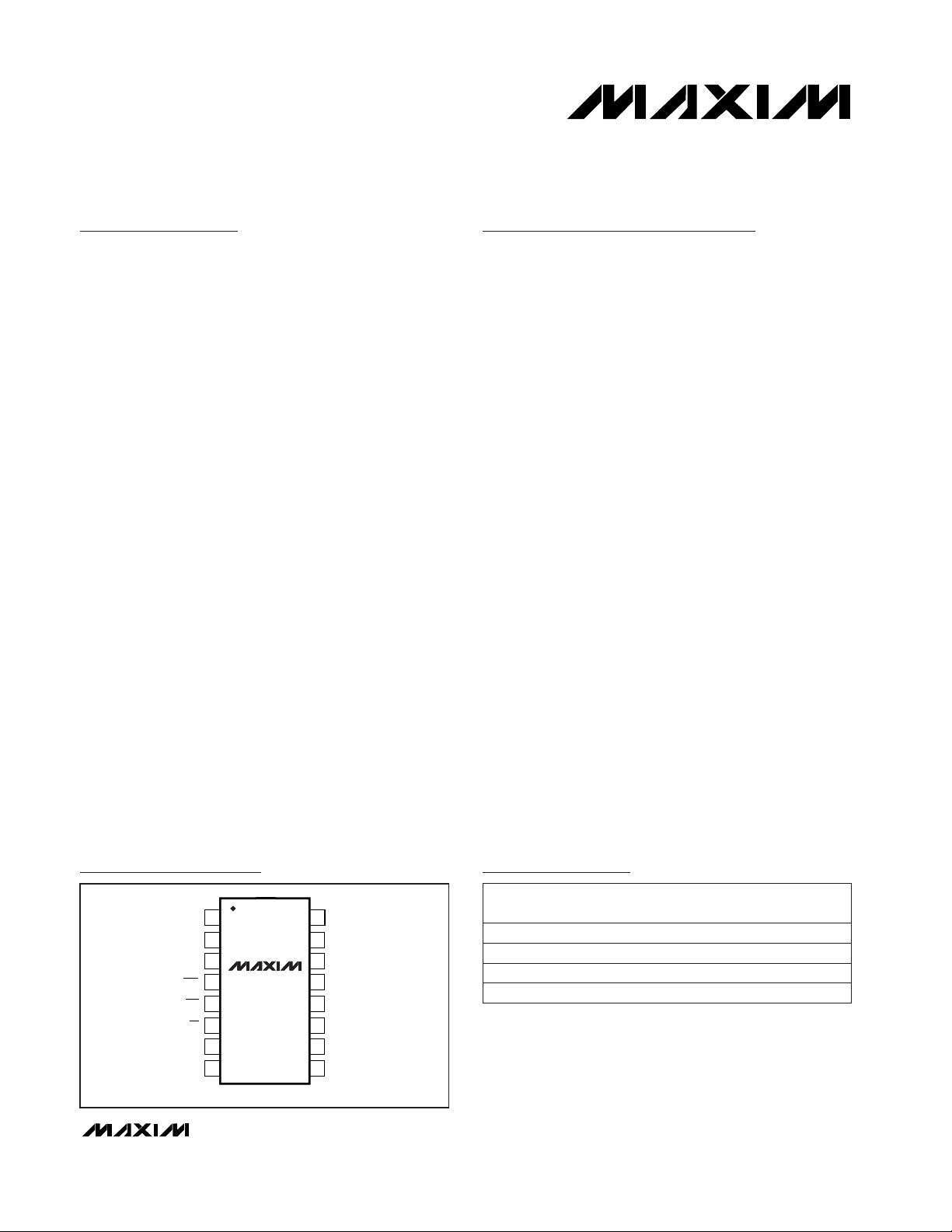
MAX5120/MAX5121
+3V/+5V, 12-Bit, Serial Voltage-Output DACs
with Internal Reference
________________________________________________________________
Maxim Integrated Products
1
16
15
14
13
12
11
10
9
1
2
3
4
5
6
7
8
OS V
DD
REFADJ
REF
AGND
PD
UPO
DOUT
DGND
TOP VIEW
MAX5120
MAX5121
QSOP
OUT
RSTVAL
CS
PDL
CLR
DIN
SCLK
19-1428; Rev 0; 2/99
PART
MAX5120AEEE
MAX5120BEEE -40°C to +85°C
-40°C to +85°C
TEMP. RANGE
PIN-
PACKAGE
16 QSOP
16 QSOP
Pin Configuration
Ordering Information
INL
(LSB)
±0.5
±1
MAX5121AEEE
MAX5121BEEE±1-40°C to +85°C
-40°C to +85°C 16 QSOP
16 QSOP ±2
SPI and QSPI are trademarks of Motorola, Inc.
MICROWIRE is a trademark of National Semiconductor Corp.
MAX5120/MAX5121
+3V/+5V, 12-Bit, Serial Voltage-Output DACs
with Internal Reference
2 _______________________________________________________________________________________
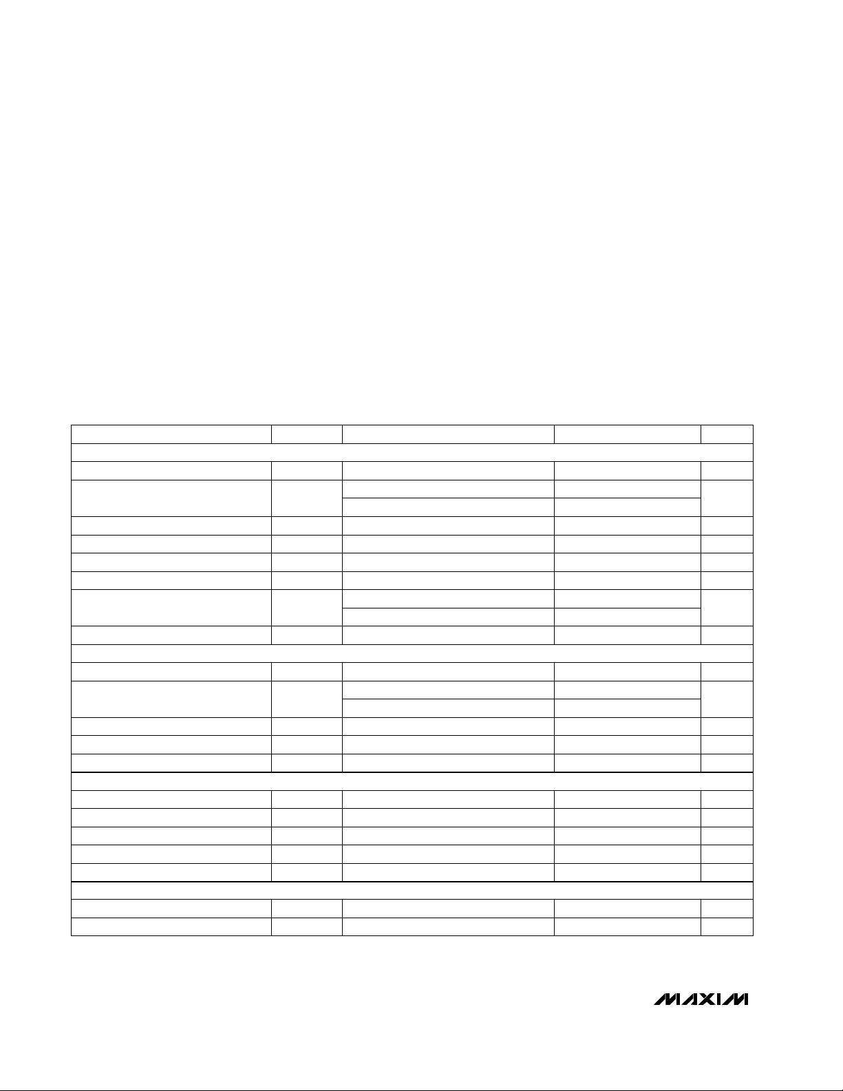
ABSOLUTE MAXIMUM RATINGS
ELECTRICAL CHARACTERISTICS—MAX5120 (+5V)
(VDD= +5V ±10%, OS = AGND = DGND = 0V, 33nF capacitor at REFADJ, internal reference, RL= 5kΩ, CL= 100pF, TA= T
MIN
to
T
MAX
, unless otherwise noted. Typical values are at TA= +25°C.)
Stresses beyond those listed under “Absolute Maximum Ratings” may cause permanent damage to the device. These are stress ratings only, and functional
operation of the device at these or any other conditions beyond those indicated in the operational sections of the specifications is not implied. Exposure to
absolute maximum rating conditions for extended periods may affect device reliability.
VDDto AGND, DGND...............................................-0.3V to +6V
AGND to DGND.....................................................-0.3V to +0.3V
Digital Inputs to DGND.............................................-0.3V to +6V
Digital Outputs (DOUT, UPO) to DGND.....-0.3V to (V
DD
+ 0.3V)
OUT to AGND.............................................-0.3V to (V
DD
+ 0.3V)
OS to AGND ...................................(AGND - 4V) to (V
DD
+ 0.3V)
REF, REFADJ to AGND..............................-0.3V to (V
DD
+ 0.3V)
Maximum Current into Any Pin............................................50mA
Continuous Power Dissipation (T
A
= +70°C)
QSOP (derate 8.00mW/°C above +70°C).....................667mW
Operating Temperature Range ..........................-40°C to +85°C
Storage Temperature Range.............................-65°C to +150°C
Lead Temperature (soldering, 10sec).............................+300°C
VIN= 0 or V
DD
MAX5120A
REFADJ = V
DD
4.5V ≤ VDD≤ 5.5V
MAX5120B
MAX5120B
MAX5120A
MAX5120A
Code = FFF hex, TA= +25°C
TA= +25°C
CONDITIONS
pF8C
IN
Input Capacitance
µA-1 0.001 1I
IN
Input Leakage Current
mV200V
HYS
Input Hysteresis
V0.8V
IL
Input Low Voltage
V3V
IH
Input High Voltage
µA3.3 7REFADJ Current
ppm/°C
10
TCV
REF
3
Output Voltage Temperature
Coefficient
V2.5V
REF
Output Voltage
-0.5 0.5
Bits12NResolution
µV/V20 250PSRRPower-Supply Rejection Ratio
ppm/°C
10 30
TCV
FS
310
Full-Scale Temperature
Coefficient (Note 3)
V4.0458 4.095 4.1442V
FS
Full-Scale Voltage
LSB-1 1DNLDifferential Nonlinearity
mV-10 10V
OS
Offset Error (Note 2)
-3 -0.2 3 mVGEGain Error
UNITSMIN TYP MAXSYMBOLPARAMETER
I
SINK
= 2mA
I
SOURCE
= 2mA
V0.13 0.4V
OL
Output Low Voltage
VVDD- 0.5V
OH
Output High Voltage
MAX5120B
LSB
-1 1
INLIntegral Nonlinearity (Note 1)
0 ≤ I
OUT
≤ 100µA (sourcing) µV/µA0.1 1V
OUT/IOUT
Reference External Load Regulation
mA4Reference Short-Circuit Current
STATIC PERFORMANCE
REFERENCE
DIGITAL INPUT
DIGITAL OUTPUTS
MAX5120/MAX5121
+3V/+5V, 12-Bit, Serial Voltage-Output DACs
with Internal Reference
_______________________________________________________________________________________ 3
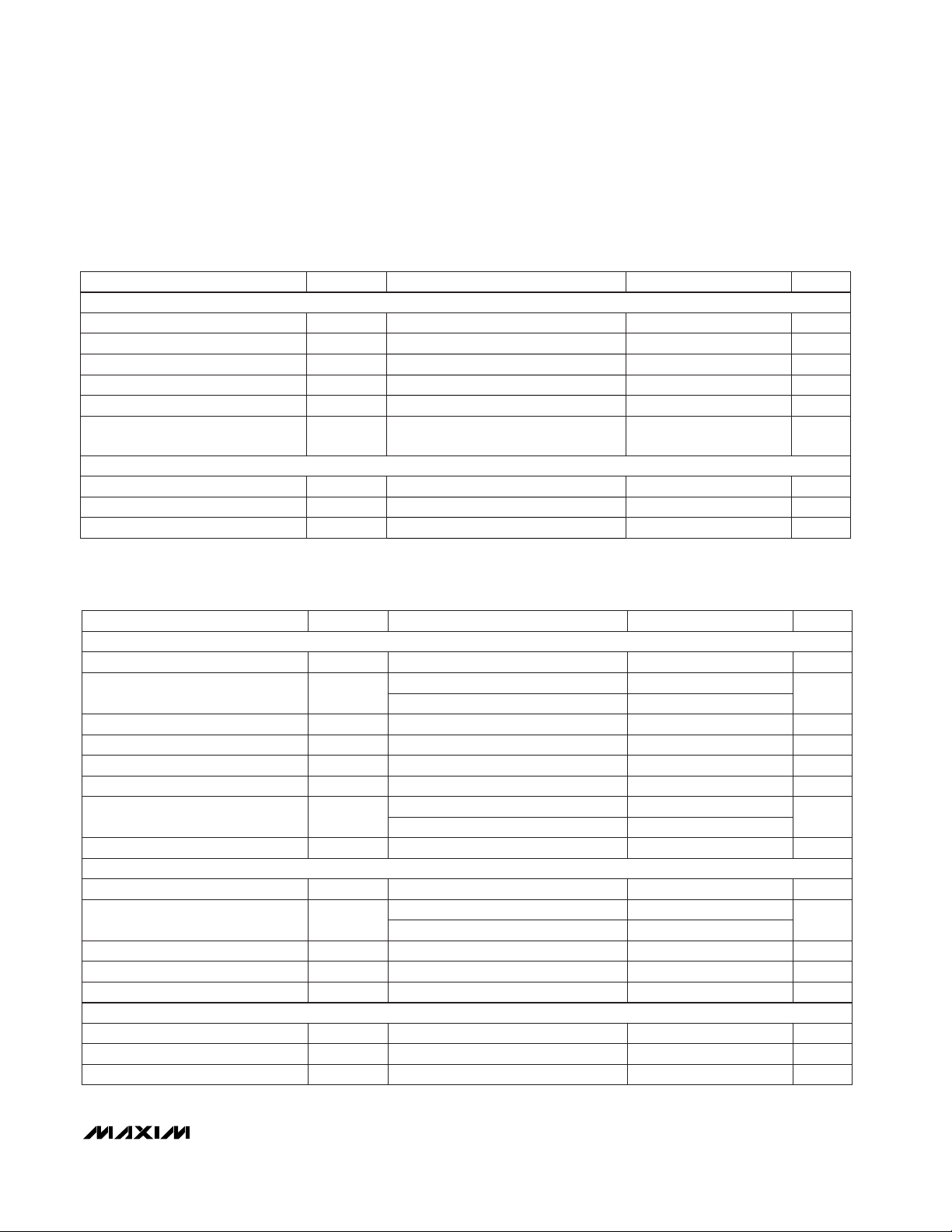
ELECTRICAL CHARACTERISTICS—MAX5120 (+5V) (continued)
(VDD= +5V ±10%, OS = AGND = DGND = 0V, 33nF capacitor at REFADJ, internal reference, RL= 5kΩ, CL= 100pF, TA= T
MIN
to
T
MAX
, unless otherwise noted. Typical values are at TA= +25°C.)
To ±0.5LSB, V
STEP
= 4V
CS = VDD, f
SCLK
= 100kHz,
V
SCLK
= 5Vp-p
CONDITIONS
µA320I
SHDN
Power-Supply Current in Shutdown
µA500 600I
DD
Power-Supply Current (Note 5)
V4.5 5.5V
DD
Power-Supply Voltage (Note 5)
nV-s5Digital Feedthrough
ms2Time Required to Exit Shutdown
kΩ83 121R
OS
OS Input Resistance
µs20Output Settling Time
V0 to V
DD
Output Voltage Swing (Note 4)
UNITSMIN TYP MAXSYMBOLPARAMETER
ELECTRICAL CHARACTERISTICS—MAX5121 (+3V)
(VDD= +3V ±10%, OS = AGND = DGND = 0V, 33nF capacitor at REFADJ, internal reference, RL= 5kΩ, CL= 100pF, TA= T
MIN
to
T
MAX
, unless otherwise noted. Typical values are at TA= +25°C.)
MAX5121A
REFADJ = V
DD
2.7V ≤ VDD≤ 3.3V
MAX5121B
MAX5121B
MAX5121A
MAX5121A
Data = FFF hex, TA= +25°C
TA= +25°C
CONDITIONS
mV200V
HYS
Input Hysteresis
V0.8V
IL
Input Low Voltage
V2.2V
IH
Input High Voltage
µA3.3 7REFADJ Current
mA4Reference Short-Circuit Current
ppm/°C
10
TCV
REF
MAX5121B
3
0 ≤ I
OUT
≤ 100µA (sourcing)
Output Voltage Temperature
Coefficient
V1.25V
REF
Output Voltage
-1 1
µV/µA0.1 1
Bits12NResolution
µV/V20 250PSRRPower-Supply Rejection Ratio
ppm/°C
10 30
TCV
FS
LSB
310
V
OUT/IOUT
Full-Scale Temperature
Coefficient (Note 3)
V2.0229 2.0475 2.0721V
FS
Full-Scale Voltage
LSB-1 1DNLDifferential Nonlinearity
mV-10 10V
OS
Offset Error (Note 2)
-5 -0.2 5
Reference External Load Regulation
mVGEGain Error
UNITSMIN TYP MAXSYMBOLPARAMETER
-2 2
INLIntegral Nonlinearity (Note 1)
V/µs0.6SRVoltage Output Slew Rate
DYNAMIC PERFORMANCE
POWER REQUIREMENTS
STATIC PERFORMANCE
REFERENCE
DIGITAL INPUT
MAX5120/MAX5121
+3V/+5V, 12-Bit, Serial Voltage-Output DACs
with Internal Reference
4 _______________________________________________________________________________________
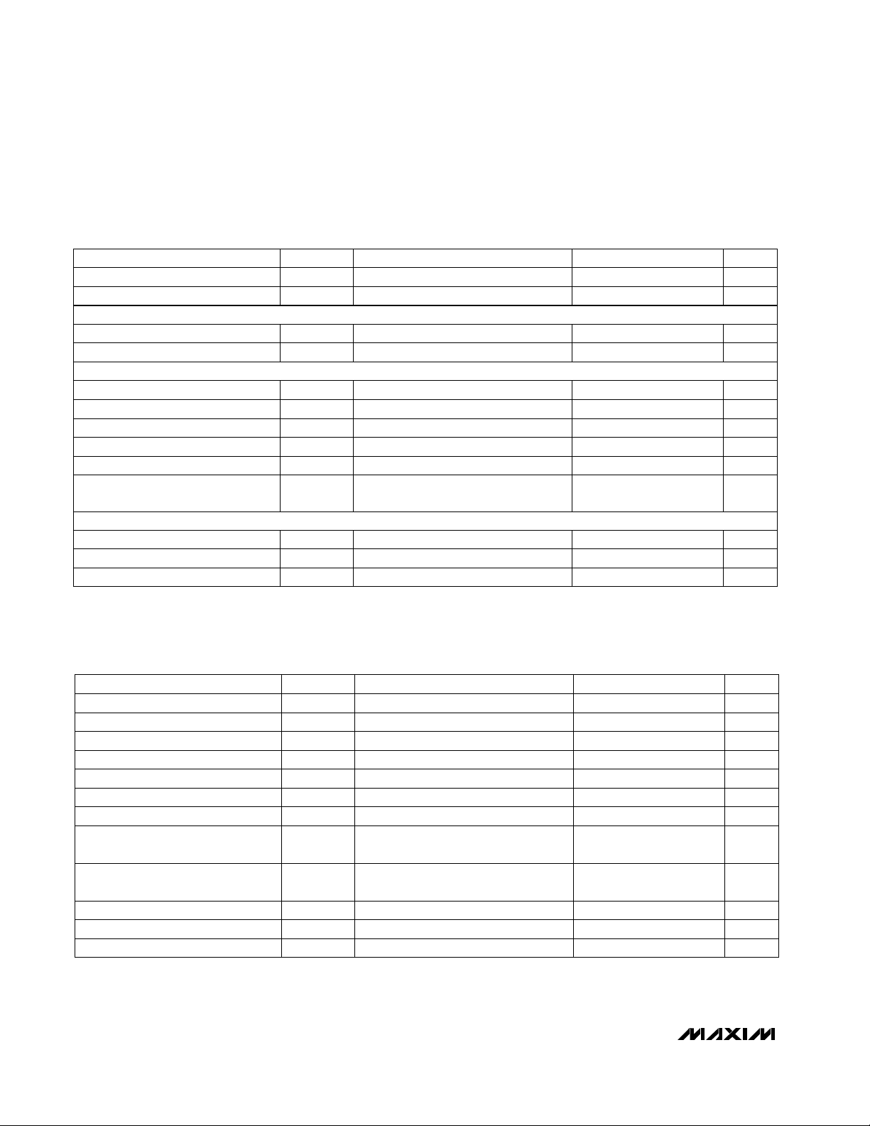
ELECTRICAL CHARACTERISTICS—MAX5121 (+3V) (continued)
(VDD= +3V ±10%, OS = AGND = DGND = 0V, 33nF capacitor at REFADJ, internal reference, RL= 5kΩ, CL= 100pF, TA= T
MIN
to
T
MAX
, unless otherwise noted. Typical values are at TA= +25°C.)
To ±0.5LSB, V
STEP
= 2V
CS = VDD, f
SCLK
= 100kHz,
V
SCLK
= 3Vp-p
CONDITIONS
µA320I
SHDN
Power-Supply Current in Shutdown
µA500 600I
DD
Power-Supply Current (Note 5)
V2.7 3.6V
DD
Power-Supply Voltage (Note 5)
nV-s5Digital Feedthrough
ms2Time Required to Exit Shutdown
kΩ83 121R
OS
OS Input Resistance
µs20Output Settling Time
V0 to V
DD
Output Voltage Swing (Note 4)
UNITSMIN TYP MAXSYMBOLPARAMETER
I
SINK
= 2mA V0.13 0.4V
OL
Output Low Voltage
I
SOURCE
= 2mA VVDD- 0.5V
OH
Output High Voltage
VIN= 0 or V
DD
µA-1 0.001 1I
IN
Input Leakage Current
pF8C
IN
Input Capacitance
V/µs0.6SRVoltage Output Slew Rate
TIMING CHARACTERISTICS—MAX5120 (+5V)
(VDD= +5V ±10%, OS = AGND = DGND = 0V, 33nF capacitor at REFADJ, internal reference, RL= 5kΩ, CL= 100pF, TA= T
MIN
to
T
MAX
, unless otherwise noted. Typical values are at TA= +25°C.)
ns40t
CSS
CS Fall to SCLK Rise Setup Time
ns40t
CL
SCLK Pulse Width Low
CONDITIONS
ns100t
CP
SCLK Clock Period
ns40t
CH
SCLK Pulse Width High
ns0t
CSH
SCLK Rise to CS Rise Hold Time
ns10t
CS0
SCLK Rise to CS Fall Delay Time
ns40t
DS
SDI Setup Time
ns0t
DH
SDI Hold Time
UNITSMIN TYP MAXSYMBOLPARAMETER
ns100t
CSW
CS Pulse Width High
ns40t
CS1
CS Rise to SCLK Rise Hold Time
C
LOAD
= 200pF ns80t
DO1
SCLK Rise to DOUT Valid
Propagation Delay Time
C
LOAD
= 200pF ns80t
DO2
SCLK Fall to DOUT Valid
Propagation Delay Time
DIGITAL OUTPUTS
POWER REQUIREMENTS
DYNAMIC PERFORMANCE
MAX5120/MAX5121
+3V/+5V, 12-Bit, Serial Voltage-Output DACs
with Internal Reference
_______________________________________________________________________________________ 5
Note 1: Accuracy is guaranteed as shown in the following table:
Note 2: Offset is measured at the code closest to 10mV.
Note 3: The temperature coefficient is determined by the “box” method in which the maximum
∆V
OUT
over the temperature range is
divided by ∆T.
Note 4: Accuracy is better than 1.0LSB for V
OUT
= 10mV to (VDD- 180mV). Guaranteed by PSR test on end points.
Note 5: R
LOAD
= ∞ and digital inputs are at either VDDor DGND.
TIMING CHARACTERISTICS—MAX5121 (+3V)
(VDD= +3V ±10%, OS = AGND = DGND = 0V, 33nF capacitor at REFADJ, internal reference, RL= 5kΩ, CL= 100pF, TA= T
MIN
to
T
MAX
, unless otherwise noted. Typical values are at TA= +25°C.)
ns60t
CSS
CS Fall to SCLK Rise Setup Time
ns150
ns
C
LOAD
= 200pF
75
t
CSW
t
CL
SCLK Pulse Width Low
CONDITIONS
ns150t
CP
SCLK Clock Period
ns75t
CH
SCLK Pulse Width High
ns0t
CSH
SCLK Rise to CS Rise Hold Time
CS Pulse Width High
ns75t
CS1
CS Rise to SCLK Rise Hold Time
C
LOAD
= 200pF ns200t
DO1
SCLK Rise to DOUT Valid
Propagation Delay Time
ns200t
DO2
SCLK Fall to DOUT Valid
Propagation Delay Time
ns10t
CS0
SCLK Rise to CS Fall Delay Time
ns60t
DS
SDI Setup Time
ns0t
DH
SDI Hold Time
UNITSMIN TYP MAXSYMBOLPARAMETER
105
203
4095
4095
Accuracy Guaranteed
To Code:From Code:
V
DD
(V)
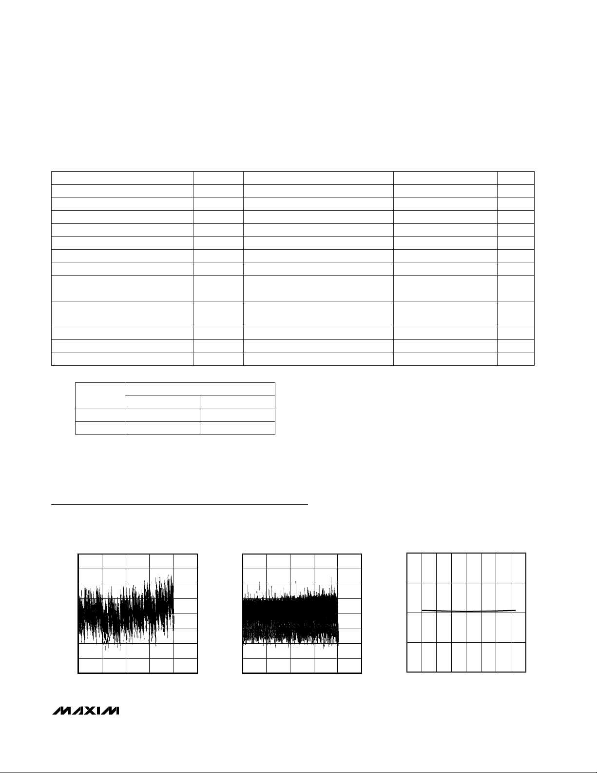
Typical Operating Characteristics
(VDD= +5V (MAX5120), VDD= +3V (MAX5121), RL= 5kΩ, CL= 100pF, OS = AGND, TA = +25°C, unless otherwise noted.)
-0.20
-0.15
-0.10
-0.05
0
0.05
0.10
0.15
0.20
0 1000 2000 3000 4000 5000
MAX5120
INTEGRAL NONLINEARITY vs.
DIGITAL INPUT CODE
MAX5120/21 toc01
DIGITAL INPUT CODE
INL (LSB)
-0.20
-0.15
-0.10
-0.05
0
0.05
0.10
0.15
0.20
0 1000 2000 3000 4000 5000
MAX5120
DIFFERENTIAL NONLINEARITY vs.
DIGITAL INPUT CODE
MAX5120/21 toc02
DIGITAL INPUT CODE
DNL (LSB)
2.490
2.495
2.500
2.505
2.510
-60 -20 20 60-40 0 40 80 100
MAX5120
REFERENCE VOLTAGE vs. TEMPERATURE
MAX5120/21 toc03
TEMPERATURE (°C)
REFERENCE VOLTAGE (V)
MAX5120/MAX5121
+3V/+5V, 12-Bit, Serial Voltage-Output DACs
with Internal Reference
6 _______________________________________________________________________________________
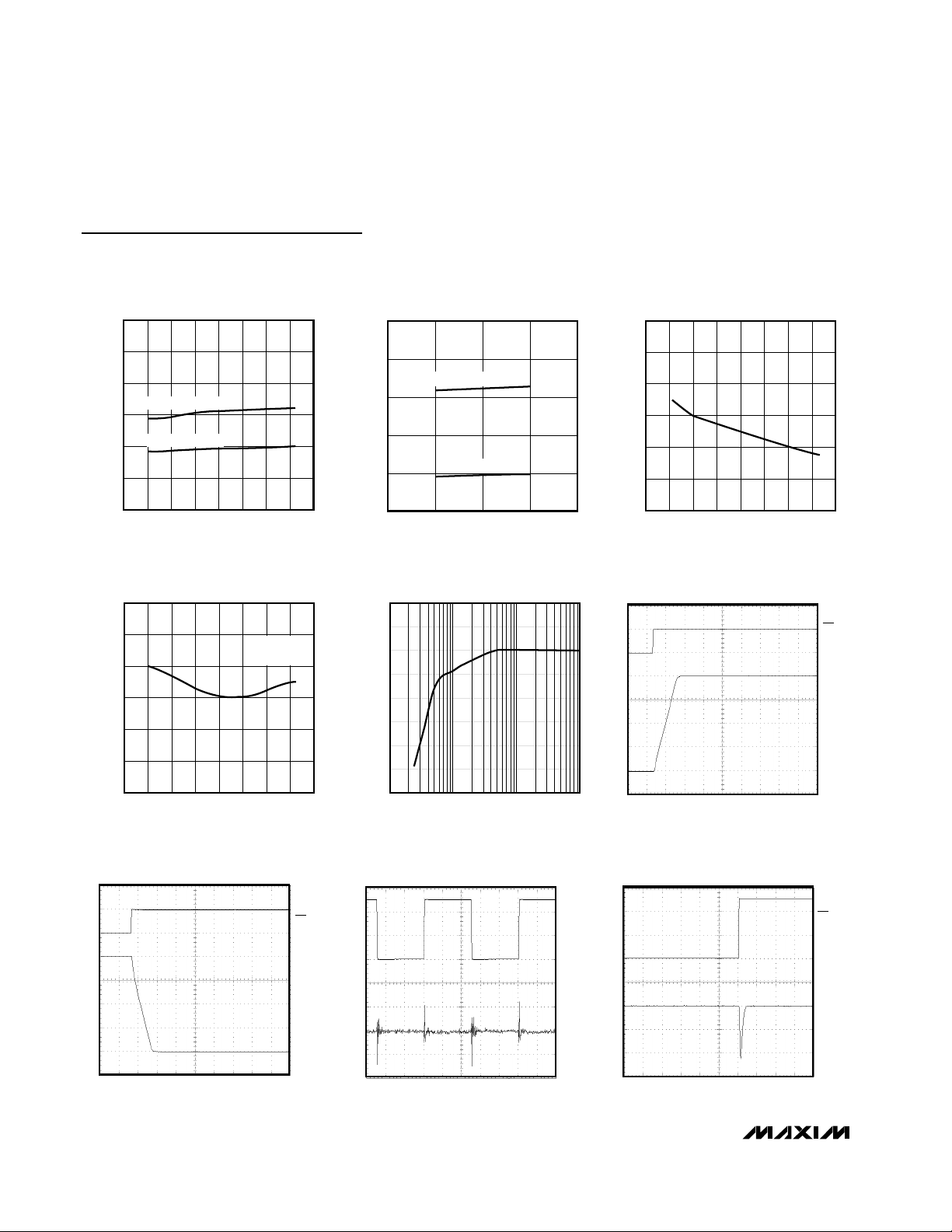
Typical Operating Characteristics (continued)
(VDD= +5V (MAX5120), VDD= +3V (MAX5121), RL= 5kΩ, CL= 100pF, OS = AGND, TA = +25°C, unless otherwise noted.)
200
250
300
350
400
450
500
-60 -20-40 0 20406080100
MAX5120
SUPPLY CURRENT vs. TEMPERATURE
MAX5120/21 toc04
TEMPERATURE (°C)
SUPPLY CURRENT (µA)
(CODE = AAA HEX)
(CODE = 000 HEX)
250
300
400
350
450
500
4.0 4.5 5.0 5.5
(CODE = AAA HEX)
(CODE = 000 HEX)
6.0
MAX5120
SUPPLY CURRENT vs. SUPPLY VOLTAGE
MAX5120/21 toc05
SUPPLY VOLTAGE (V)
SUPPLY CURRENT (µA)
1.0
1.5
2.0
2.5
3.0
3.5
4.0
-60 -20-40 0 20406080100
MAX5120
SHUTDOWN CURRENT vs. TEMPERATURE
MAX5120/21 toc06
TEMPERATURE (°C)
SHUTDOWN CURRENT (µA)
4.093
4.094
4.095
4.096
4.097
4.098
4.099
-60 -20-40 0 20406080100
MAX5120
FULL-SCALE OUTPUT vs. TEMPERATURE
MAX5120/21 toc07
TEMPERATURE (°C)
FULL-SCALE OUTPUT (V)
RL = 5kΩ
C
L
= 100pF
CS
5V/div
OUT
1V/div
5µs/div
MAX5120
DYNAMIC RESPONSE FALL TIME
MAX5120/21-10
0.1 1 10 100
MAX5120
FULL-SCALE ERROR vs. RESISTIVE LOAD
MAX5120/21 toc08
RL (kΩ)
FULL-SCALE ERROR (LSB)
0.50
-1.50
-1.25
-1.00
-0.75
-0.50
-0.25
0
0.25
CS
5V/div
OUT
1V/div
5µs/div
MAX5120
DYNAMIC RESPONSE RISE TIME
MAX5120/21-09
SCLK
2V/div
OUT
1mV/div
AC COUPLED
2µs/div
MAX5120
DIGITAL FEEDTHROUGH (SCLK, OUT)
MAX5120/21-11
CS
2V/div
OUT
100mV/div
AC COUPLED
5µs/div
MAX5120
MAJOR CARRY TRANSITION
MAX5120/21-12
 Loading...