

Page 1
General Description
The MAX5109 dual 8-bit digital-to-analog converters
(DACs) feature nonvolatile registers. These nonvolatile
registers store the DAC operating modes and output
states, allowing the DACs to initialize to specified configurations at power-up.
Precision on-chip output buffers swing rail-to-rail, and
provide 8µs settling time. The I2C*-compatible, 2-wire
serial interface allows for a maximum clock frequency
of 400kHz.
The MAX5109 has independent high and low reference
inputs allowing maximum output voltage range flexibility. The reference rails accept voltage inputs that range
from ground to the positive supply rail.
This device operates from a single +2.7V to +5.25V supply and consumes 200µA per DAC. A software-controlled power-down mode decreases supply current to
less than 25µA. A software-controlled mute mode sets
each DAC, or both DACs simultaneously, to their respective REFL_ voltages. The MAX5109 also includes an
asynchronous MUTE input, that drives both DAC outputs
simultaneously to their respective REFL_ voltages.
The MAX5109 is available in a 16-pin QSOP and is
specified for operation over the extended (-40°C to
+85°C) temperature range.
Applications
Digital Gain and Offset Adjustments
Programmable Attenuators
Portable Instruments
Power-Amp Bias Control
ATE Calibration
Laser Biasing
Features
♦ Nonvolatile Registers Initialize DACs to Stored
States
♦ +2.7V to +5.25V Single-Supply Operation
♦ Dual 8-Bit DACs with Independent High and Low
Reference Inputs
♦ Rail-to-Rail Output Buffers
♦ Low 200µA per DAC Supply Current
♦ Power-Down Mode Reduces Supply Current to
25µA (max)
♦ 400kHz, I
2
C-Compatible, 2-Wire Serial Interface
♦ Asynchronous MUTE Input
♦ Small 16-Pin QSOP Package
MAX5109
Nonvolatile, Dual, 8-Bit DACs with 2-Wire Serial
Interface
________________________________________________________________ Maxim Integrated Products 1
Ordering Information
19-3585; Rev 0; 2/05
For pricing, delivery, and ordering information, please contact Maxim/Dallas Direct! at
1-888-629-4642, or visit Maxim’s website at www.maxim-ic.com.
PART TEMP RANGE PIN-PACKAGE
-40°C to +85°C 16 QSOP
*Purchase of I2C components from Maxim Integrated Products, Inc., or one of its sublicensed Associate Companies, conveys a
license under the Philips I
2
C Patent Rights to use these components in an I2C system, provided that the system conforms to the I2C
Standard Specification defined by Philips.
Pin Configuration and Typical Operating Circuit appear at
end of data sheet.
DAC0
NONVOLATILE/
VOLATILE
REGISTERS
DAC1
NONVOLATILE/
VOLATILE
REGISTERS
REFL0
OUT0
OUT1
SCL
GND
V
DD
SDA
A2
A1
A0
2-WIRE
SERIAL
INTERFACE/
CONTROL
MUTE
REFH0
REFL1
REFH1
MAX5109
DAC0
DAC1
A3
Simplified Diagram
MAX5109EEE
Page 2
MAX5109
Nonvolatile, Dual, 8-Bit DACs with 2-Wire Serial
Interface
2 _______________________________________________________________________________________
ABSOLUTE MAXIMUM RATINGS
Stresses beyond those listed under “Absolute Maximum Ratings” may cause permanent damage to the device. These are stress ratings only, and functional
operation of the device at these or any other conditions beyond those indicated in the operational sections of the specifications is not implied. Exposure to
absolute maximum rating conditions for extended periods may affect device reliability.
(All voltages referenced to GND, unless otherwise noted.)
V
DD
, A0, A1, A2, A3, SCL, SDA, MUTE.................-0.3V to +6.0V
OUT0, OUT1, REFH0, REFH1
REFL0, REFL1 .......................................-0.3V to (V
DD
+ 0.3V)
Maximum Current into Any Pin .........................................±50mA
Power Dissipation (T
A
= +70°C)
16-Pin QSOP (derate 8.3mW/°C above +70°C)...........667mW
Operating Temperature Range ...........................-40°C to +85°C
Junction Temperature .....................................................+150°C
Storage Temperature Range .............................-60°C to +150°C
Lead Temperature (soldering, 10s) .................................+300°C
ELECTRICAL CHARACTERISTICS
(VDD= +2.7V to +5.25V, GND = 0, REFH_ = VDD, REFL_ = GND, R
LOAD
= 5kΩ, CL = 100pF, TA= -40°C to +85°C, unless otherwise
noted. Typical values are at V
DD
= +3.0V and TA= +25°C.) (Note 1)
PARAMETER
CONDITIONS
UNITS
STATIC ACCURACY
Resolution 8 Bits
Code range 0A hex to F0 hex ±1
Integral Nonlinearity INL
Full code range ±2
LSB
Code range 0A hex to F0 hex
Differential Nonlinearity (Note 2) DNL
Full code range ±1
LSB
Offset Error ZCE Code = 0A hex
mV
Offset Temperature Coefficient Code = 0A hex
µV/°C
Gain Error Code = F0 hex (Note 3) ±1 LSB
Gain-Error Temperature
Coefficient
Code = F0 hex
LSB/°C
Power-Supply Rejection Ratio PSRR
Code = FF hex or 0A hex, V
REFH_
= 2.5V,
V
REFL_
= 0, f = DC
1
LSB/V
REFERENCE INPUT (REFH_, REFL_)
Input Voltage Range
V
REFH_
,
V
REFL_
V
REFH_
≥ V
REFL_
0
V
Input Resistance
600 kΩ
Input-Resistance Temperature
Coefficient
ppm/°C
Input Capacitance 10 pF
DAC OUTPUTS (OUT_)
Load Regulation Code = F0 hex, R
LOAD
≥ 5kΩ
±1 LSB
Output Leakage DAC powered down, not muted
µA
Amplifier Output Resistance 0.5V ≤ V
OUT_
≤ (VDD - 0.5V) 0.5 Ω
DIGITAL INPUTS (A_, MUTE)
2.7V ≤ VDD < 3.6V
0.7 x
Input High Voltage (Note 4) V
IH
3.6V ≤ VDD ≤ 5.25V
V
SYMBOL
MIN TYP MAX
±0.5
320 460
V
DD
2.52
±20
±0.002
±35
±0.5
±20
V
DD
±10
Page 3

MAX5109
Nonvolatile, Dual, 8-Bit DACs with 2-Wire Serial
Interface
_______________________________________________________________________________________ 3
ELECTRICAL CHARACTERISTICS (continued)
(VDD= +2.7V to +5.25V, GND = 0, REFH_ = VDD, REFL_ = GND, R
LOAD
= 5kΩ, CL = 100pF, TA= -40°C to +85°C, unless otherwise
noted. Typical values are at V
DD
= +3.0V and TA= +25°C.) (Note 1)
PARAMETER
CONDITIONS
UNITS
2.7V ≤ VDD < 3.6V
0.3 x
Input Low Voltage (Note 4) V
IL
3.6V ≤ VDD ≤ 5.25V 1.1
V
Input Hysteresis V
HYS
0.05 x
V
Input Leakage Current I
IN
VIN = 0 or V
DD
±1 µA
Input Capacitance C
IN
10 pF
DIGITAL OUTPUT (SDA)
I
SINK
= 3mA 0.4
Output Low Voltage V
OL
I
SINK
= 6mA 0.6
V
Tri-State Leakage I
L
±1 µA
Tri-State Output Capacitance C
OUT
15 pF
DYNAMIC PERFORMANCE
SCL to OUT_ Settling t
COS
(Note 5) 8 µs
Crosstalk V
REFH_
= 2.5V
P-P
at 10kHz (Note 6) 55 dB
V
REFH_
= 2.5V
P-P
at 1kHz 65
Multiplying Signal-to-Noise Plus
Distortion
SINAD
V
REFH_
= 2.5V
P-P
at 10kHz 52
dB
Multiplying Bandwidth V
REFH_
= 0.5V
P-P
, 3dB bandwidth 325 kHz
Reference Feedthrough V
REFH_
= 2.5V
P-P
at f = 10kHz (Note 7) 88 dB
Clock Feedthrough 2.5 nVs
Output Noise e
N
800
nV/√Hz
Power-Up Time t
SDR
From power-down state 4 µs
Power-Down Time t
SDN
1.5 µs
INTERFACE PORTS (SCL, SDA)
V
IL
0.3 x
Input Voltage
V
IH
0.7 x
V
Input Hysteresis V
HYS
0.05 x
V
Input Current I
IN
±1 µA
Input Capacitance C
IN
5pF
POWER SUPPLIES
Power-Supply Voltage V
DD
V
Normal operation 0.4 0.7
Supply Current I
DD
I
LOAD
= 0, digital
inputs at GND or
V
DD
During nonvolatile
write
2
mA
Power-Down Current 25 µA
SYMBOL
MIN TYP MAX
V
DD
V
DD
V
DD
2.70 5.25
V
DD
V
DD
Page 4
MAX5109
Nonvolatile, Dual, 8-Bit DACs with 2-Wire Serial
Interface
4 _______________________________________________________________________________________
ELECTRICAL CHARACTERISTICS (continued)
(VDD= +2.7V to +5.25V, GND = 0, REFH_ = VDD, REFL_ = GND, R
LOAD
= 5kΩ, CL = 100pF, TA= -40°C to +85°C, unless otherwise
noted. Typical values are at V
DD
= +3.0V and TA= +25°C.) (Note 1)
PARAMETER
SYMBOL
CONDITIONS
MIN
TYP
MAX
UNITS
DIGITAL TIMING (Figure 3, Note 8)
SCL Clock Frequency f
SCL
kHz
Setup Time for START Condition
t
SU:STA
0.6 µs
Hold Time for START Condition t
HD:STA
0.6 µs
SCL High Time t
HIGH
0.6 µs
SCL Low Time t
LOW
1.3 µs
Data Setup Time t
SU:DAT
100 ns
Data Hold Time
0 0.9 µs
SDA, SCL Rise Time t
R
ns
SDA, SCL Fall Time t
F
ns
Setup Time for STOP Condition t
SU:STO
0.6 µs
Bus Free Time Between a STOP
and START Condition
t
BUF
1.3 µs
Pulse Width of Spike Suppressed
t
SP
50 ns
Maximum Capacitive Load for
Each Bus Line
C
B
(Note 9)
pF
Write NV Register Busy Time (Note 10) 15 ms
NONVOLATILE MEMORY RELIABILITY
Data Retention TA= +85°C50
Years
TA= +25°C
Endurance
T
A
= +85°C
Stores
Note 1: All devices are 100% production tested at TA = +25°C. All temperature limits are guaranteed by design.
Note 2: Guaranteed monotonic.
Note 3: Gain error is defined as:
where V
F0,Meas
is the DAC voltage with input code F0 hex and V
F0,Ideal
is the ideal DAC voltage with input code F0 hex or
(V
REFH
- V
REFL
) x (240 / 256) + V
REFL
.
Note 4: The device draws higher supply current when the digital inputs are driven with voltages between (V
DD
- 0.5V) and (GND +
0.5V). See Supply Current vs. Digital Input Voltage in the Typical Operating Characteristics.
Note 5: Output settling time is measured from the 50% point of the rising edge of the last SCL of the data byte to 0.5 LSB of OUT_’s
final value for a code transition from 10 hex to F0 hex.
Note 6: Crosstalk is defined as the coupling from a DAC switching from code 00 hex to code FF hex to any other DAC that is in a
steady state at code 00 hex.
Note 7: Reference feedthrough is defined as the coupling from one driven reference with input code = FF hex to any other DAC out-
put with the reference of the DAC at a constant value and input code = 00 hex.
Note 8: SCL clock period includes rise and fall times t
R
and tF. All digital input signals are specified with tR= tF= 2ns and timed
from a voltage level of (V
IL
+ VIH) / 2.
Note 9: An appropriate bus pullup resistance must be selected depending on board capacitance. Refer to the document linked to
this web address: www.semiconductors.philips.com/acrobat/literature/9398/39340011.pdf.
Note 10:The busy time begins from the initiation of the stop pulse.
256
00
×−−()
,,
_
V ZCE V
V
F Meas F Ideal
REFH
400
t
HD:DAT
300
300
400
200,000
50,000
Page 5
MAX5109
Nonvolatile, Dual, 8-Bit DACs with 2-Wire Serial
Interface
_______________________________________________________________________________________ 5
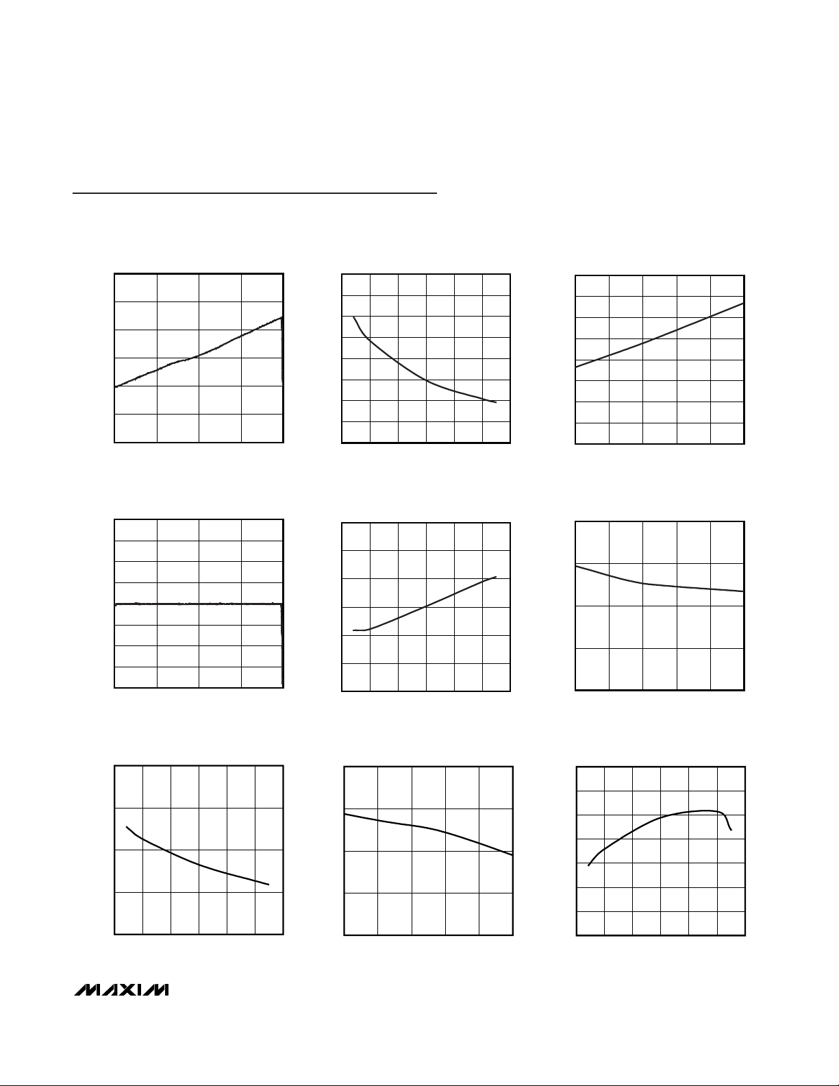
INTEGRAL NONLINEARITY
vs. INPUT CODE
MAX5109 toc01
INPUT CODE
INTEGRAL NONLINEARITY (LSB)
19212864
-0.5
0
0.5
1.0
1.5
2.0
-1.0
0 256
INTEGRAL NONLINEARITY
vs. SUPPLY VOLTAGE
MAX5109 toc02
SUPPLY VOLTAGE (V)
INTEGRAL NONLINEARITY (LSB)
5.04.53.0 3.5 4.0
0.25
0.50
0.75
1.00
1.25
1.50
1.75
2.00
0
2.5 5.5
INTEGRAL NONLINEARITY
vs. TEMPERATURE
MAX5109 toc03
TEMPERATURE (°C)
INTEGRAL NONLINEARITY (LSB)
6035-15 10
0.25
0.50
0.75
1.00
1.50
1.25
1.75
2.00
0
-40 85
DIFFERENTIAL NONLINEARITY
vs. INPUT CODE
MAX5109 toc04
INPUT CODE
DIFFERENTIAL NONLINEARITY (LSB)
19212864
-0.75
-0.50
-0.25
0
0.25
0.50
0.75
1.00
-1.00
0 256
DIFFERENTIAL NONLINEARITY
vs. SUPPLY VOLTAGE
MAX5109 toc05
SUPPLY VOLTAGE (V)
DIFFERENTIAL NONLINEARITY (LSB)
5.04.54.03.53.0
-1.25
-1.00
-0.75
-0.50
-0.25
0
-1.50
2.5 5.5
DIFFERENTIAL NONLINEARITY
vs. TEMPERATURE
MAX5109 toc06
TEMPERATURE (°C)
DIFFERENTIAL NONLINEARITY (LSB)
603510-15
-1.1
-1.0
-0.9
-0.8
-1.2
-40 85
OFFSET ERROR vs. SUPPLY VOLTAGE
MAX5109 toc07
SUPPLY VOLTAGE (V)
OFFSET ERROR (LSB)
5.04.54.03.53.0
0.2
0.3
0.4
0.5
0.1
2.5 5.5
OFFSET ERROR vs. TEMPERATURE
MAX5109 toc08
TEMPERATURE (°C)
OFFSET ERROR (LSB)
603510-15
0.25
0.30
0.35
0.40
0.20
-40 85
GAIN ERROR vs. SUPPLY VOLTAGE
MAX5109 toc09
SUPPLY VOLTAGE (V)
GAIN ERROR (LSB)
5.04.54.03.53.0
-0.18
-0.16
-0.14
-0.12
-0.10
-0.08
-0.06
-0.20
2.5 5.5
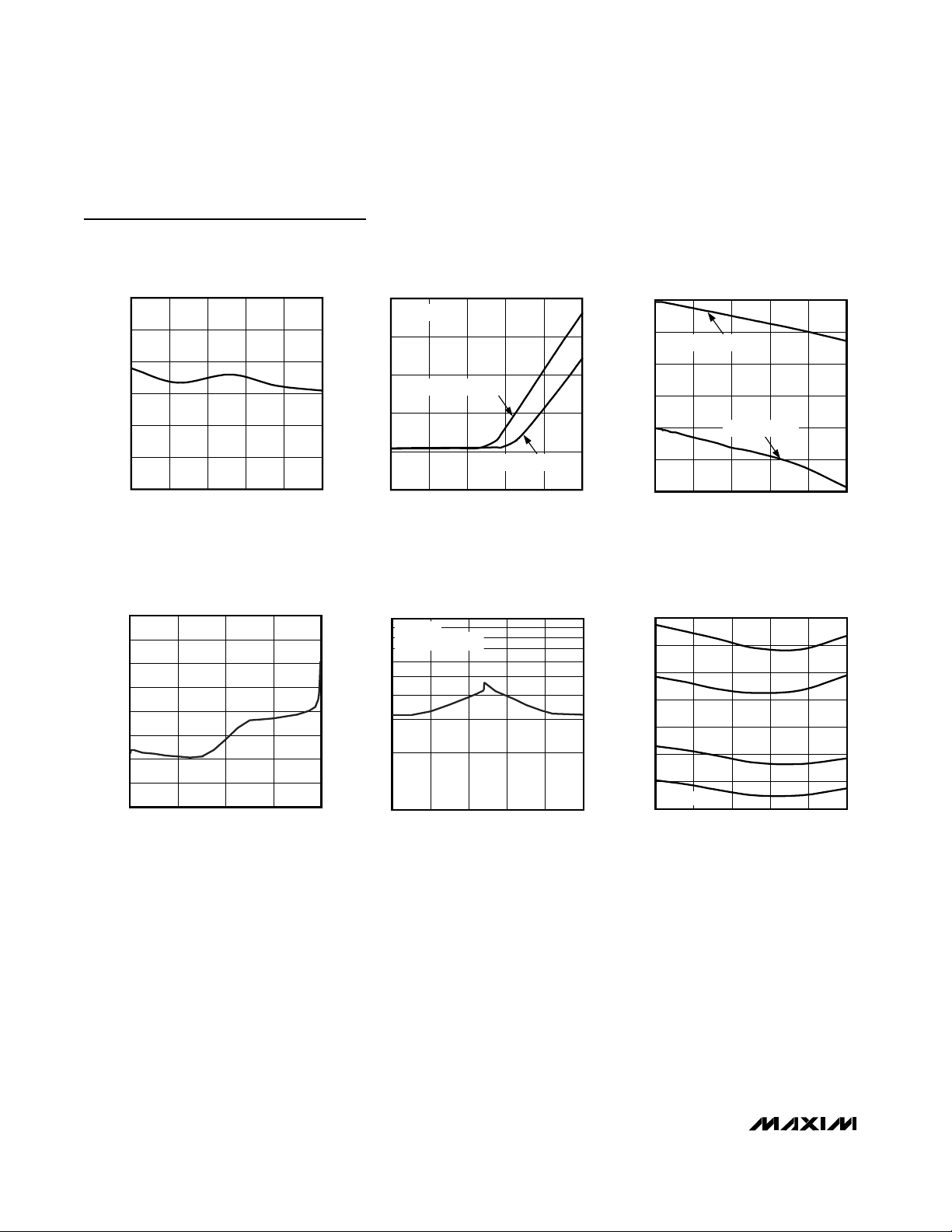
Typical Operating Characteristics
(VDD= +3V, V
REFH_
= +3V, V
REFL_
= GND, RL= 5kΩ, CL= 100pF, TA= +25°C, unless otherwise noted.)
Page 6
MAX5109
Nonvolatile, Dual, 8-Bit DACs with 2-Wire Serial
Interface
6 _______________________________________________________________________________________
GAIN ERROR vs. TEMPERATURE
MAX5109 toc10
TEMPERATURE (°C)
GAIN ERROR (LSB)
603510-15
-0.18
-0.16
-0.14
-0.12
-0.10
-0.08
-0.20
-40 85
OFFSET OUTPUT VOLTAGE
vs. OUTPUT SINK CURRENT
MAX5109 toc11
OUTPUT SINK CURRENT (mA)
OFFSET OUTPUT VOLTAGE (V)
8642
0.20
0.25
0.30
0.35
0.40
0.15
010
VDD = V
REFH_
= 5V
V
REFL_
= 0.2V
VDD = V
REFH_
= 3V
FULL-SCALE OUTPUT VOLTAGE
vs. OUTPUT SOURCE CURRENT
MAX5109 toc12
OUTPUT SOURCE CURRENT (mA)
FULL-SCALE OUTPUT VOLTAGE (V)
12963
2.5
3.0
3.5
4.0
4.5
5.0
2.0
015
VDD = V
REFH_
= 5V
VDD = V
REFH_
= 3V
SUPPLY CURRENT
vs. INPUT CODE
MAX5109 toc13
INPUT CODE
SUPPLY CURRENT (µA)
19212864
275
300
325
350
375
400
425
450
250
0 256
NO LOAD
SUPPLY CURRENT
vs. DIGITAL INPUT VOLTAGE
MAX5109 toc14
DIGITAL INPUT VOLTAGE (V)
SUPPLY CURRENT (µA)
1000
100
NO LOAD
V
DD
= V
REFH_
= +5V
123405
SUPPLY CURRENT vs. TEMPERATURE
MAX5109 toc15
TEMPERATURE (°C)
SUPPLY CURRENT (µA)
603510-15
240
260
280
300
320
340
360
220
-40 85
NO LOAD
A
B
C
D
A: V
DD
= 5V, V
REFH_
= 4.096V, CODE = FFh
B: V
DD
= 5V, V
REFH_
= 4.096V, CODE = 00h
C: V
DD
= 3V, V
REFH_
= 2.5V, CODE = FFh
D: V
DD
= 3V, V
REFH_
= 2.5V, CODE = 00h
Typical Operating Characteristics (continued)
(VDD= +3V, V
REFH_
= +3V, V
REFL_
= GND, RL= 5kΩ, CL= 100pF, TA= +25°C, unless otherwise noted.)
Page 7

SUPPLY CURRENT
vs. SUPPLY VOLTAGE
MAX5109 toc16
SUPPLY VOLTAGE (V)
SUPPLY CURRENT (µA)
5.04.54.03.53.0
240
260
280
300
320
340
360
220
2.5 5.5
NO LOAD
CODE 00h
TA = -40°C
TA = +85°C
TA = +25°C
SUPPLY CURRENT
vs. REFERENCE VOLTAGE
MAX5109 toc17
REFERENCE VOLTAGE (V)
SUPPLY CURRENT (µA)
431 2
225
250
275
300
325
350
375
400
200
05
NO LOAD
V
DD
= 5V
CODE = FFh
VDD = 5V
CODE = 00h
VDD = 3V
CODE = FFh
VDD = 3V
CODE = 00h
REFERENCE FEEDTHROUGH
vs. FREQUENCY
MAX5109 toc18
FREQUENCY (kHz)
REFERENCE FEEDTHROUGH (dB)
10,00010001001010.1
-90
-80
-70
-60
-50
-40
-100
0.01 100,000
VDD = 5V
VDD = 3V
MEASURED AT OUT1,
V
REFL1
= V
REFL0
= GND,
V
REFH1
= V
DD,
V
REFH0
= 2.5V
P-P
,
SIGNAL CENTERED AT V
DD
/2,
OUT0 = FFh,
OUT1 = 00h,
NO LOAD
MAX5109
Nonvolatile, Dual, 8-Bit DACs with 2-Wire Serial
Interface
_______________________________________________________________________________________ 7
STARTUP GLITCH
MAX5109 toc19
NV REGISTER PREVIOUSLY SET TO CODE FFh
GND
GND
OUT_
1V/div
V
DD
2V/div
100µs/div
POWER-DOWN TRANSITION
MAX5109 toc20
GND
GND
OUT_
500mV/div
SCL
2V/div
400ns/div
26
POWER-UP TRANSITION
MAX5109 toc21
GND
GND
OUT_
500mV/div
SCL
2V/div
1µs/div
25
26 27
POSITIVE CARRY TRANSITION
MAX5109 toc22
OUT_
50mV/div
AC-COUPLED
4µs/div
NEGATIVE CARRY TRANSITION
MAX5109 toc23
OUT_
50mV/div
AC-COUPLED
2µs/div
POSITIVE SETTLING TIME
MAX5109 toc24
OUT_
1V/div
2µs/div
SCL
2V/div
GND
GND
25
26 27
Typical Operating Characteristics (continued)
(VDD= +3V, V
REFH_
= +3V, V
REFL_
= GND, RL= 5kΩ, CL= 100pF, TA= +25°C, unless otherwise noted.)
Page 8

MAX5109
Nonvolatile, Dual, 8-Bit DACs with 2-Wire Serial
Interface
8 _______________________________________________________________________________________
Pin Description
PIN NAME FUNCTION
1 A3 Address Select 3. Connect to VDD or GND to set the device address.
2 A2 Address Select 2. Connect to VDD or GND to set the device address.
3 A1 Address Select 1. Connect to VDD or GND to set the device address.
4 A0 Address Select 0. Connect to VDD or GND to set the device address.
5 REFH1 DAC1 High Reference Input. REFH1 must be equal to or greater than REFL1.
6 REFL1 DAC1 Low Reference Input. REFL1 must be equal to or less than REFH1.
7 OUT1 DAC1 Output. OUT1 is buffered with a unity-gain amplifier.
8 GND Ground
9 MUTE
Active-Low Mute Input. Connect MUTE low to drive all DAC outputs to their respective reference low
voltages. Connect MUTE to V
DD
for normal operation.
10 N.C. No Connection. Not internally connected.
11 OUT0 DAC0 Output. OUT0 is buffered with a unity-gain amplifier.
12 REFL0 DAC0 Low Reference Input. REFL0 must be equal to or less than REFH0.
13 REFH0 DAC0 High Reference Input. REFH0 must be equal to or greater than REFL0.
14 SCL Serial Clock Input. Connect SCL to VDD through a 2.4kΩ pullup resistor.
15 V
DD
Positive Power Input. Connect VDD to a +2.7 to +5.25V power supply. Bypass VDD to GND with a 0.1µF
capacitor as close to the device as possible.
16 SDA Serial Data Input/Output. Connect SDA to VDD through a 2.4kΩ pullup resistor.
Typical Operating Characteristics (continued)
(VDD= +3V, V
REFH_
= +3V, V
REFL_
= GND, RL= 5kΩ, CL= 100pF, TA= +25°C, unless otherwise noted.)
OUTPUT CROSSTALK
MAX5109 toc27
OUT1
10mV/div
AC-COUPLED
2µs/div
SCL
2V/div
GND
GND
OUT0
2V/div
OUT1_ SET TO 7Fh
CLOCK FEEDTHROUGH
MAX5109 toc26
OUT_
10mV/div
AC-COUPLED
1µs/div
SCL
2V/div
GND
OUT_ SET TO 7Fh
NEGATIVE SETTLING TIME
MAX5109 toc25
OUT_
1V/div
2µs/div
SCL
2V/div
GND
GND
25
26 27
Page 9

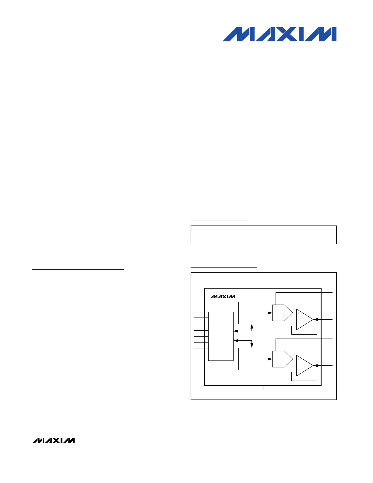
Detailed Description
The MAX5109 8-bit DACs feature internal, nonvolatile
registers that store the DAC states for initialization during power-up. This device consists of resistor-string
DACs, rail-to-rail output buffers, a shift register, poweron reset (POR) circuitry, and volatile and nonvolatile
memory registers (Figure 1). The shift register decodes
the control and address bits, routing the data to the
proper registers. Writing data to a selected volatile register immediately updates the DAC outputs.
The volatile registers retain data as long as the device
is powered. Removing power clears the volatile registers. The nonvolatile registers retain data even after
power is removed. On startup, when power is first
applied, data from the nonvolatile registers is transferred to the volatile registers to automatically initialize
the device. Read data from the nonvolatile or volatile
registers using the 2-wire serial interface.
DAC Operation
The MAX5109 uses a DAC matrix decoding architecture that saves power. A resistor string divides the difference between the external reference voltages,
V
REFH_
and V
REFL_
. Row and column decoders select
the appropriate tap from the resistor string, providing
the equivalent analog voltage. The resistor string presents a code-independent input impedance to the reference and guarantees a monotonic output. Figure 2
shows a simplified diagram of one DAC.
Output Buffer Amplifiers
The MAX5109 analog outputs are internally buffered by
precision unity-gain amplifiers. The outputs swing from
GND to V
DD
with a V
REFL_
-to-V
REFH_
output transition.
The amplifier outputs typically settle to ±0.5 LSB in 8µs
when loaded with 5kΩ in parallel with 100pF.
MAX5109
Nonvolatile, Dual, 8-Bit DACs with 2-Wire Serial
Interface
_______________________________________________________________________________________ 9
DAC0
NONVOLATILE
REGISTER
DAC1
NONVOLATILE
REGISTER
REFL0
OUT0
9
14
15
8
16
13
12
11
5
6
7
1
2
3
OUT1
SCL
GND
V
DD
SDA
A3
A2
A1
2-WIRE
SERIAL
INTERFACE/
CONTROL
MUTE
REFH0
REFL1
REFH1
DAC0
VOLATILE
REGISTER
DAC1
VOLATILE
REGISTER
MAX5109
DAC0
DAC1
4
A0
POR
Figure 1. MAX5109 Functional Diagram
REFH_
REFL_
R1
R15
R16
R255
R0
D7
D6
D5
D4
DAC
MSB DECODER
D3
D0
D2 D1
LSB DECODER
Figure 2. DAC Simplified Circuit Diagram
Page 10

MAX5109
DAC Registers
The MAX5109 features two registers per DAC, a volatile
and a nonvolatile register, that store the DAC data. The
volatile DAC register holds the current value of each
DAC. Write data to the volatile registers directly from
the 2-wire serial interface or by loading the previously
stored data from the respective nonvolatile register.
Clear the volatile registers by removing power to the
device. The volatile registers are read/write.
The nonvolatile register retains the DAC values even
after power is removed. Read stored data using the 2wire serial interface. On power-up, the device is automatically initialized with data stored in the nonvolatile
registers. The nonvolatile registers are read/write and
programmed to all zeros at the factory.
Serial Interface
The MAX5109 features an I2C-compatible, 2-wire serial
interface consisting of a bidirectional serial data line
(SDA) and a serial clock line (SCL). SDA and SCL facilitate bidirectional communication between the
MAX5109 and the master at rates up to 400kHz (Figure
3). The master (typically a microcontroller) initiates data
transfer on the bus and generates SCL. SDA and SCL
require pullup resistors (2.4kΩ or greater; see the Typical
Operating Circuit). Optional resistors (24Ω) in series with
SDA and SCL protect the device inputs from high-voltage spikes on the bus lines. Series resistors also minimize crosstalk and undershoot of the bus signals.
I2C Compatibility
The MAX5109 is compatible with existing I2C systems.
SCL and SDA are high-impedance inputs; SDA has an
open-drain output. The Typical Operating Circuit shows
an I2C application. The communication protocol supports standard I2C 8-bit communications. The general
call address is ignored, and CBUS formats are not sup-
ported. The device’s address is compatible with 7-bit
I
2
C addressing protocol only. No 10-bit address for-
mats are supported.
Bit Transfer
One data bit transfers during each SCL rising edge.
Nine clock cycles are required to transfer the data into
or out of the MAX5109. The data on SDA must remain
stable during the high period of the SCL clock pulse.
Changes in SDA while SCL is high are read as control
signals (see the START and STOP Conditions section).
Both SDA and SCL idle high.
START and STOP Conditions
The master initiates a transmission with a START condition (S), a high-to-low transition on SDA with SCL high.
The master terminates a transmission with a STOP condition (P), a low-to-high transition on SDA while SCL is
high (Figure 4). A START condition from the master signals the beginning of a transmission to the MAX5109.
The master terminates transmission by issuing a STOP
condition. The STOP condition frees the bus. If a
REPEATED START condition (Sr) is generated instead
of a STOP condition, the bus remains active.
Nonvolatile, Dual, 8-Bit DACs with 2-Wire Serial
Interface
10 ______________________________________________________________________________________
t
HD:STA
t
HIGH
t
R
t
F
t
HD:STA
S Sr ACK
SCL
SDA
t
SU:STA
t
SU:STO
t
R
t
F
t
BUF
t
LOW
t
SU:DAT
t
HD:DAT
PS
PARAMETERS ARE MEASURED FROM 30% TO 70%.
Figure 3. 2-Wire Serial-Interface Timing Diagram
SPSr
SCL
SDA
Figure 4. START and STOP Conditions
Page 11

Early STOP Conditions
The MAX5109 recognizes a STOP condition at any
point during transmission except if a STOP condition
occurs in the same high pulse as a START condition
(Figure 5). This condition is not a legal I2C format.
REPEATED START Conditions
A REPEATED START (Sr) condition is used when the
bus master is writing to several I2C devices and does
not want to relinquish control of the bus. The MAX5109
serial interface supports continuous write operations
with an Sr condition separating them. Continuous read
operations require Sr conditions because of the change
in direction of data flow.
Acknowledge Bit (ACK) and Not-
Acknowledge Bit (NACK)
Successful data transfers are acknowledged with an
acknowledge bit (ACK) or a not-acknowledge bit
(NACK). Both the master and the MAX5109 (slave) generate acknowledge bits. To generate an acknowledge,
the receiving device must pull SDA low before the rising
edge of the acknowledge-related clock pulse (ninth
pulse) and keep it low during the high period of the
clock pulse (Figure 6). To generate a not acknowledge,
the receiver allows SDA to be pulled high before the rising edge of the acknowledge-related clock pulse and
leaves it high during the high period of the clock pulse.
Monitoring the acknowledge bits allows for detection of
unsuccessful data transfers. An unsuccessful data
transfer happens if a receiving device is busy or if a
system fault has occurred. In the event of an unsuccessful data transfer, the master should reattempt communication at a later time.
Slave Address
A master initiates communication with a slave device
by issuing a START condition followed by a slave
address (Figure 7). The slave address consists of 7
address bits and a read/write bit (R/W). When idle, the
device continuously waits for a START condition followed by its slave address. When the device recognizes its slave address, it acquires the data byte and
executes the command. The first 3 bits (MSBs) of the
slave address have been factory programmed and are
always 010. Connect A3–A0 to VDDor GND to program
MAX5109
Nonvolatile, Dual, 8-Bit DACs with 2-Wire Serial
Interface
______________________________________________________________________________________ 11
SCL
SDA
STOP START
SCL
SDA
ILLEGAL
STOP
START
ILLEGAL EARLY STOP CONDITION
LEGAL STOP CONDITION
Figure 5. Early STOP Conditions
189
ACKNOWLEDGE
NOT ACKNOWLEDGE
SCL
S
SDA
Figure 6. Acknowledge and Not-Acknowledge Bits
SCL
SDA
123
0
A3
10
894567
A2 A1 A0
R/W
ACK
ACKNOWLEDGE
S
Figure 7. Slave Address Byte
Page 12

MAX5109
the remaining 4 bits of the slave address. The least significant bit (LSB) of the address byte (R/W) determines
whether the master is writing to or reading from the
MAX5109. (R/W = 0 selects a write condition. R/W = 1
selects a read condition.) After receiving the address,
the MAX5109 (slave) issues an acknowledge by pulling
SDA low for one clock cycle.
Write Cycle
The write command requires 27 clock cycles. In write
mode (R/W = 0), the command byte that follows the
address byte controls the MAX5109 (Table 1). For a
write function, set bits C7 and C6 to zero. Set bits C5
and C4 to select the volatile or nonvolatile register
(Table 2). Set bits C3–C0 to select the respective DAC
register (Table 3). The registers update on the rising
edge of the 26th SCL pulse. Prematurely aborting the
write cycle does not update the DAC. See Table 4 for a
summary of the write commands.
Read Cycle
A read command requires 36 clock cycles. In read
mode, the MAX5109 sends the contents of the volatile
and nonvolatile registers to the bus. Reading a register
requires a REPEATED START (Sr) condition. To read a
register first, write a read command (R/W = 0, Figure 8).
Set the most significant 2 bits of the command byte to
10 (C7 = 1 and C6 = 0). Set bits C5 and C4 to read
from either the volatile or nonvolatile register (Table 5).
Set bits C3–C0 to select the desired DAC register
(Table 6). After the command byte, send a Sr condition
followed by the address of the device (R/W = 1). The
MAX5109 then acknowledges and sends the data to
the bus.
Nonvolatile, Dual, 8-Bit DACs with 2-Wire Serial
Interface
12 ______________________________________________________________________________________
S0
1
0
A3
A2
A1
A0
A3
A2
A1
A0
1 0 NV V R3R2R1R0
C7 C6 C5 C4 C3 C2 C1 C0
Sr 0
1
0
MSB LSB
MSB LSB
LSBMSB
ACK
ACK
ACK
NACK
R/W
= 1
D7 D6
D5
D4
D3 D2 D1 D0 P
MSB LSB
ADDRESS AND COMMAND BYTES GENERATED BY MASTER DEVICE
DATA BYTE GENERATED BY MAX5109
NACK GENERATED BY
MASTER DEVICE
R/W
= 0
Figure 8. Example Read Word Data Sequence
ADDRESS BYTE COMMAND BYTE DATA BYTE
START
C7C6C5C4C3C2C1C
D7D6D5D4D3D2D1D
STOP
Master
SDA
A3A2A1A
C7C6N
R3R2R1R
D7–D0 P
Slave
SDA
A
C
A
C
A
C
Table 1. Write Operation
S010
R/W
0
0
K
V
0
V
0
K
0
K
Page 13

Mute/Power-Down Mode
The MAX5109 features software-controlled mute and
power-down modes for each DAC. The power-down
mode places the DAC output in a high-impedance
state and reduces quiescent-current consumption
(25µA (max) with all DACs powered-down).
Mute drives the selected DAC output to the corresponding REFL_ voltage. The volatile DAC registers retain data
and the output returns to its previous state when mute is
disabled. The MAX5109 also features an asynchronous
MUTE input that mutes all DACs simultaneously.
The volatile and nonvolatile registers remain active
while the MAX5109 is in mute and/or power-down
modes. Writing to or reading from the volatile or nonvolatile registers does not remove the MAX5109 from
mute or power-down mode. Writing or transferring data
to the volatile registers while the device is muted or
powered down updates the DAC outputs to the new
state upon exiting mute or power-down mode.
MAX5109
Nonvolatile, Dual, 8-Bit DACs with 2-Wire Serial
Interface
______________________________________________________________________________________ 13
NONVOLATILE
(NV)
VOLATILE
(V)
FUNCTION
00
Transfer data from NVREG_ to
VREG_
0 1 Write to VREG_
1 0 Write to NVREG_
1 1 Write to NVREG and VREG_
Table 2. Volatile and Nonvolatile Write
Selection
R3
R1
FUNCTION
0 0 0 0 DAC0
0 0 0 1 DAC1
1 1 1 1 All DACs*
Table 3. DAC Write Selection
*This option is only valid for a write to all volatile registers.
DATA BYTE
ADDRESS
BYTE
COMMAND BYTE
COMMAND
S
T
A
R
A
C7C6C5C4C3C2C1C
A
A
STOP
Write VREG_
R3R2R1R
D7–D0 P
Write All
VREG_*
D7–D0 P
Write
NVREG_
R3R2R1R
D7–D0 P
Write VREG_
and NVREG_
R3R2R1R
D7–D0 P
Transfer
NVREG_ to
VREG_
R3R2R1R
— P
Table 4. Write-Command Summary
*This option is only valid for a write to all volatile registers.
C
K
T
S 0 0001
S 0 00011111
R/W
C
K
0
0
R2
MSB LSB
D7D6D5D4D3D2D1D
R0
0
C
K
S 0 0010
S 0 0011
S 0 0000
0
0
0
Page 14

MAX5109
Mute/Power-Down Register and Operation
Separate nonvolatile and volatile control registers store
and update the state of the mute/power-down mode for
each DAC. Tables 7 and 8 show how to access and
control each register. Register access is gained by setting control bits C3–C0 to 0100. Bits C5 and C4 indicate whether the nonvolatile or volatile control register
is accessed. The volatile register maintains data while
the device remains powered. The nonvolatile register
maintains data even after power is removed. The
MAX5109 starts up (power first applied) by transferring
the mute/power-down modes from the nonvolatile con-
trol register to the volatile control register. The nonvolatile control register is set to 00 hex at the factory.
Power-On Reset
Power-on reset (POR) circuitry controls the initialization
of the MAX5109. A POR loads the volatile registers with
the data stored in the nonvolatile registers.
This initialization period takes 500µs (typ). During this
time, the DAC outputs are held in mute mode. At the
completion of the initialization period, the DAC outputs
update in accordance with the data stored in the nonvolatile registers.
Nonvolatile, Dual, 8-Bit DACs with 2-Wire Serial
Interface
14 ______________________________________________________________________________________
NONVOLATILE
(NV)
VOLATILE
(V)
FUNCTION
0 1 Read from VREG_
1 0 Read from NVREG_
Table 5. Volatile and Nonvolatile Read
Selection
R3
R1
FUNCTION
0 0 0 0 DAC0
0 0 0 1 DAC1
Table 6. DAC Read Selection
DATA BYTE
ADDRESS
BYTE
COMMAND BYTE
MSB
COMMAND
S
T
A
R
R/
A
C7C6C5C4C3C2C1C
A
D7D6D5D4D3D2D1D
A
STOP
Write VCTL
Control register* P
Write NVCTL
Control register* P
Write VCTL
and NVCTL
Control register* P
Transfer
NVCTL to
VCTL
Control register* P
Table 7. Mute/Power-Down Operation
*See Mute/Power-Down Control Register (Table 8).
X = Don’t care.
BIT IN REGISTER
D7
(MSB)
D6 D5 D4 D3 D2 D1
D0
(LSB)
CONTROLLING
FUNCTION
XX
XX
Power-down
DAC1
Power-down
DAC0
Table 8. Mute/Power-Down Control Register
C
K
T
S 0 00010100
S 0 00100100
S 0 00110100
S 0 00000100
W
C
K
0
R2
R0
LSB
C
K
0
Mute DAC1 Mute DAC0
Page 15

DAC Data
The 8-bit DAC data is decoded as offset binary, MSB
first, with 1 LSB = (V
REFH_
- V
REFL_
) / 256, and converted into the corresponding analog voltage as shown in
Table 9.
Applications Information
DAC Linearity and Offset Voltage
The output buffer can have a negative input offset voltage that would normally drive the output negative, but
with no negative supply, the output remains at GND
(Figure 9). Determine linearity using the end-point
method, measuring between code 10 (0A hex) and
code 240 (F0 hex) after calibrating the offset and gain
error (Figure 9).
External Voltage Reference
The MAX5109 features two reference inputs for each
DAC (REFH_ and REFL_). REFH_ sets the full-scale voltage, while REFL_ sets the zero code output. A 460kΩ
typical input impedance is independent of the code.
Power Sequencing
The voltage applied to REFH_ and REFL_ should not
exceed VDDat any time. If proper power sequencing is
not possible, connect an external Schottky diode
between REFH_, REFL_, and VDDto ensure compliance
with the absolute maximum ratings. Do not apply signals
to the digital inputs before the device is fully powered.
Power-Supply Bypassing and
Ground Management
Digital or AC transient signals on GND can create noise
at the analog output. Return GND to the highest-quality
ground available. Bypass VDD, REFH_, and REFL_ to
GND with a 0.1µF capacitor, located as close to the
device as possible. Careful PC board ground layout
minimizes crosstalk between the DAC outputs and digital inputs.
MAX5109
Nonvolatile, Dual, 8-Bit DACs with 2-Wire Serial
Interface
______________________________________________________________________________________ 15
DAC
CODE
OUTPUT
VOLTAGE (V)
1111 1111
1000 0000
0000 0001
0000 0000 V
REFL_
Table 9. Unipolar Code Output Voltage
O
DAC CODE
NEGATIVE
OFFSET
OUTPUT
VOLTAGE
Figure 9. Effect of Negative Offset (Single Supply)
255
256
×−
+
()
__
_
VV
V
REFH REFL
REFL
128
256
×−
+
(
__
_
VV
V
REFH REFL
REFL
256
−
+
()
__
_
VV
V
REFH REFL
REFL
Page 16

MAX5109
Nonvolatile, Dual, 8-Bit DACs with 2-Wire Serial
Interface
16 ______________________________________________________________________________________
RPR
P
V
DD
V
DD
V
DD
µ
C
SDA SCL
SDA
REFH0
SCL
V
DD
OUT0
OUT1
R
S
*
R
S
*
R
S
*
R
S
*
REFH1
REFL0
REFL1
A2
A1
A0
MUTE
SDA
REFH
REFH0
SCL
OUT0
OUT1REFH1
REFL
REFL0
REFL1
A0
MUTE
ADDRESS
0101 111
ADDRESS
0101 110
*OPTIONAL
MAX5109
MAX5109
A3
A2
A1
A3
Typical Operating Circuit
TOP VIEW
16
15
14
13
12
11
10
9
1
2
3
4
5
6
7
8
A3 SDA
V
DD
SCL
REFH0
REFL0
OUT0
N.C.
MUTE
MAX5109
QSOP
A2
A1
REFL1
A0
REFH1
OUT1
GND
Pin Configuration
Chip Information
TRANSISTOR COUNT: 40,209
PROCESS: BiCMOS
Page 17

MAX5109
Nonvolatile, Dual, 8-Bit DACs with 2-Wire Serial
Interface
Maxim cannot assume responsibility for use of any circuitry other than circuitry entirely embodied in a Maxim product. No circuit patent licenses are
implied. Maxim reserves the right to change the circuitry and specifications without notice at any time.
Maxim Integrated Products, 120 San Gabriel Drive, Sunnyvale, CA 94086 408-737-7600 ____________________ 17
© 2005 Maxim Integrated Products Printed USA is a registered trademark of Maxim Integrated Products, Inc.
MAX5109
Package Information
(The package drawing(s) in this data sheet may not reflect the most current specifications. For the latest package outline information,
go to www.maxim-ic.com/packages
.)
QSOP.EPS
E
1
1
21-0055
PACKAGE OUTLINE, QSOP .150", .025" LEAD PITCH
 Loading...