For free samples & the latest literature: http://www.maxim-ic.com, or phone 1-800-998-8800.
For small orders, phone 1-800-835-8769.
General Description
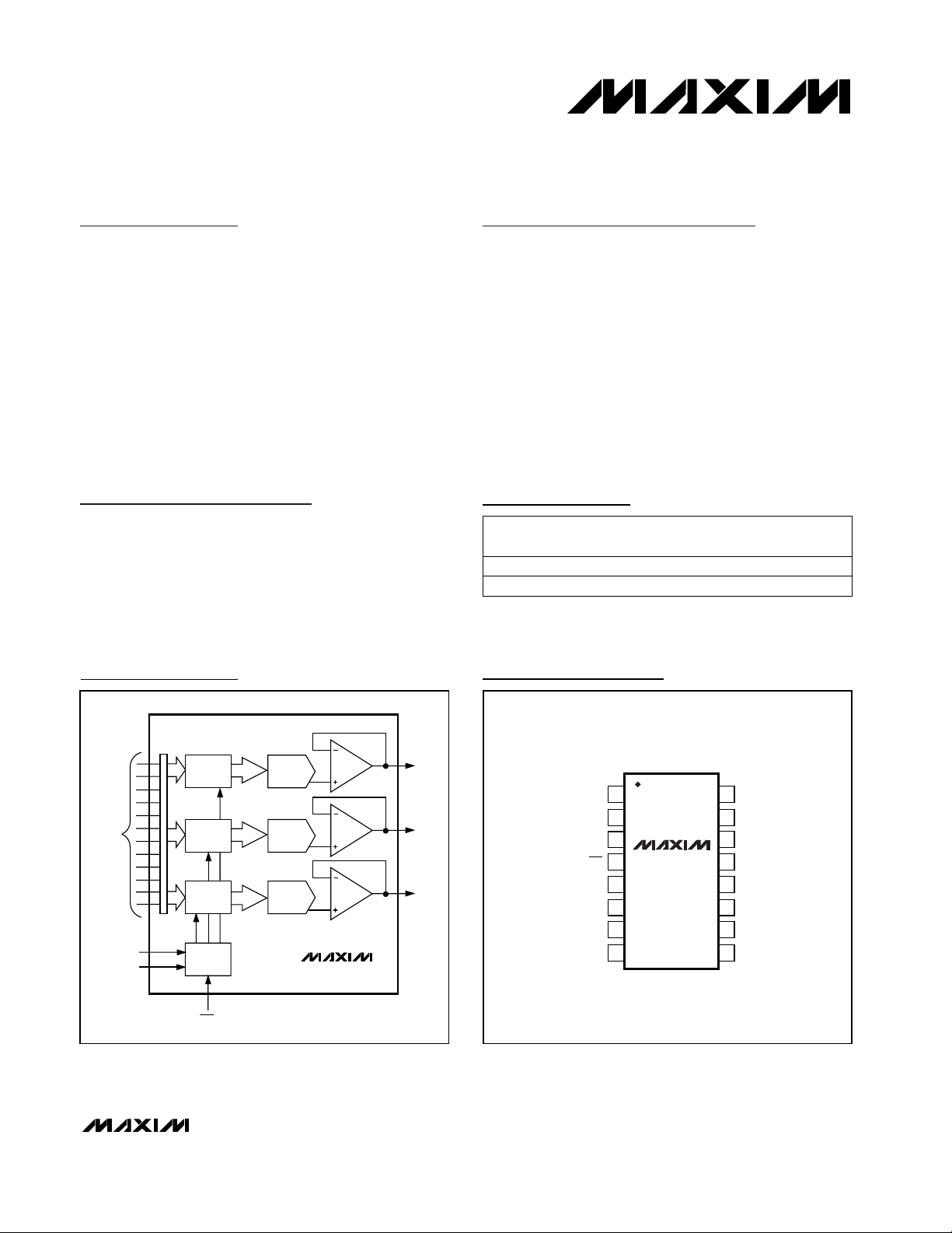
The MAX5101 parallel-input, voltage-output, triple 8-bit
digital-to-analog converter (DAC) operates from a single +2.7V to +5.5V supply and comes in a space-saving 16-pin TSSOP package. Internal precision buffers
swing Rail-to-Rail®. For all three DACs, the internal reference voltage is tied to VDD.
The MAX5101 has separate input latches for each of its
three DACs. Data is transferred to the input latches
from a common 8-bit input port. The DACs are individually selected through address inputs A0 and A1 and
are updated by bringing WR low.
The MAX5101 features a 1µA software shutdown mode,
as well as a power-on reset mode that resets all registers to code 00 hex on power-up.
Applications
Digital Gain and Offset Adjustment
Programmable Attenuators
Portable Instruments
Power-Amp Bias Control
Features
♦ +2.7V to +5.5V Single-Supply Operation
♦ Ultra-Low Supply Current
0.3mA while Operating
1µA in Software Shutdown Mode
♦ Ultra-Small 16-Pin TSSOP Package
♦ Output Buffer Amplifiers Swing Rail-to-Rail
♦ Power-On Reset Sets All Registers to Zero
MAX5101
+2.7V to +5.5V, Low-Power, Triple, Parallel
8-Bit DAC with Rail-to-Rail Voltage Outputs
________________________________________________________________ Maxim Integrated Products 1
19-1560; Rev 0; 10/99
PART
MAX5101AEUE
MAX5101BEUE -40°C to +85°C
-40°C to +85°C
TEMP. RANGE
PIN-
PACKAGE
16 TSSOP
16 TSSOP
Pin Configuration
Ordering Information
INL
(LSB)
±1
±2
Rail-to-Rail is a registered trademark of Nippon Motorola, Ltd.
Functional Diagram
OUTB
OUTC
DAC B
DAC C
INPUT
LATCH B
CONTROL
LOGIC
A0
D0–D7
WR
OUTA
DAC A
INPUT
LATCH A
A1
INPUT
LATCH C
MAX5101
TOP VIEW
1
OUTB OUTC
OUTA
2
V
3
DD
4
WR
D7
5
D6
6
D5
7
D4
8
16
15
GND
14
A0
MAX5101
TSSOP
13
A1
12
D0
D1
11
10
D2
9
D3

MAX5101
+2.7V to +5.5V, Low-Power, Triple, Parallel
8-Bit DAC with Rail-to-Rail Voltage Outputs
2 _______________________________________________________________________________________
ABSOLUTE MAXIMUM RATINGS
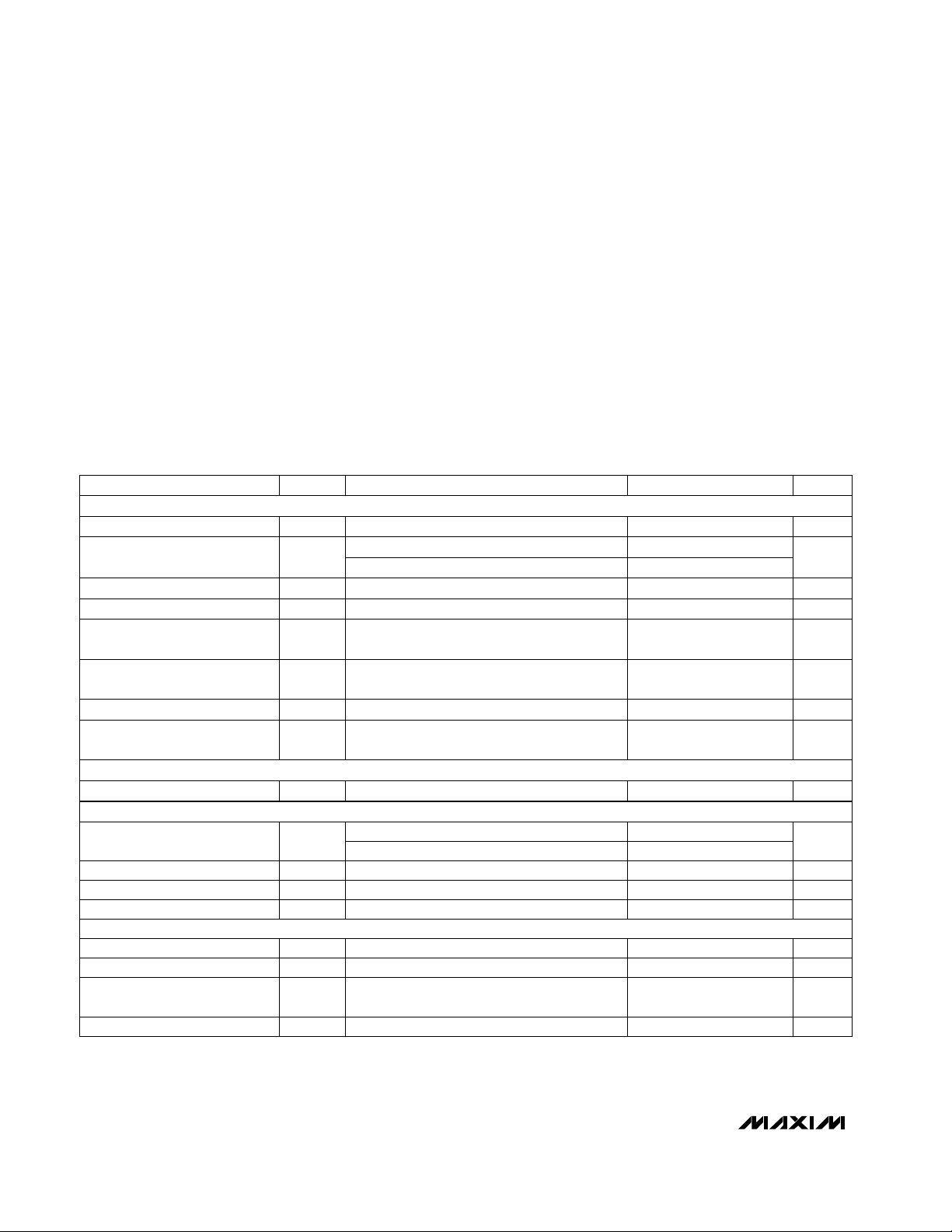
ELECTRICAL CHARACTERISTICS
(VDD= +2.7V to +5.5V, RL= 10kΩ, CL= 100pF, TA= T
MIN
to T
MAX
, unless otherwise noted. Typical values are at VDD= +3V and
T
A
= +25°C.)
Stresses beyond those listed under “Absolute Maximum Ratings” may cause permanent damage to the device. These are stress ratings only, and functional
operation of the device at these or any other conditions beyond those indicated in the operational sections of the specifications is not implied. Exposure to
absolute maximum rating conditions for extended periods may affect device reliability.
VDDto GND..............................................................-0.3V to +6V
D_, A_, WR to GND ..................................................-0.3V to +6V
OUT_ to GND ...........................................................-0.3V to V
DD
Maximum Current into Any Pin .........................................±50mA
Continuous Power Dissipation (T
A
= +70°C)
16-Pin TSSOP (derate 5.7mW/°C above +70°C) ..........457mW
Operating Temperature Range
MAX5101_EUE .................................................-40°C to +85°C
Maximum Junction Temperature .....................................+150°C
Storage Temperature Range .............................-65°C to +150°C
Lead Temperature (soldering, 10sec) .............................+300°C
Code 00 to code FF hex
MAX5101A
Code 00 to code FF hex
To 1/2LSB, from code 10 to code F0 hex
From code 00 to code F0 hex
VIN= VDDor GND
Code = F0 hex
VDD= 2.7V to 3.6V
Code = F0 hex
Code = 00 hex
MAX5101B
Guaranteed monotonic
Code = 00 hex
Code = 00 hex, VDD= 2.7V to 5.5V
RL= ∞
CONDITIONS
nVs0.5Digital Feedthrough (Note 5)
nVs500
Channel-to-Channel Isolation
(Note 4)
µs6Output Settling Time (Note 3)
V/µs0.6Output Voltage Slew Rate
pF10C
IN
Input Capacitance
µA±1.0I
IN
Input Current
V0.8V
IL
Input Low Voltage
V
2
V
IH
Input High Voltage
V0V
DD
Output Voltage Range
LSB
±2
INLIntegral Nonlinearity (Note 1)
Bits8Resolution
LSB/°C±0.001
Gain-Error Temperature
Coefficient
%±1Gain Error (Note 2)
µV/°C±10
Zero-Code Temperature
Coefficient
LSB±1DNLDifferential Nonlinearity (Note 1)
mV±20ZCEZero-Code Error
mV10
Zero-Code-Error Supply
Rejection
UNITSMIN TYP MAXSYMBOLPARAMETER
±1
VDD= 3.6V to 5.5V 3
STATIC ACCURACY
DAC OUTPUTS
DIGITAL INPUTS
DYNAMIC PERFORMANCE

MAX5101
+2.7V to +5.5V, Low-Power, Triple, Parallel
8-Bit DAC with Rail-to-Rail Voltage Outputs
_______________________________________________________________________________________ 3
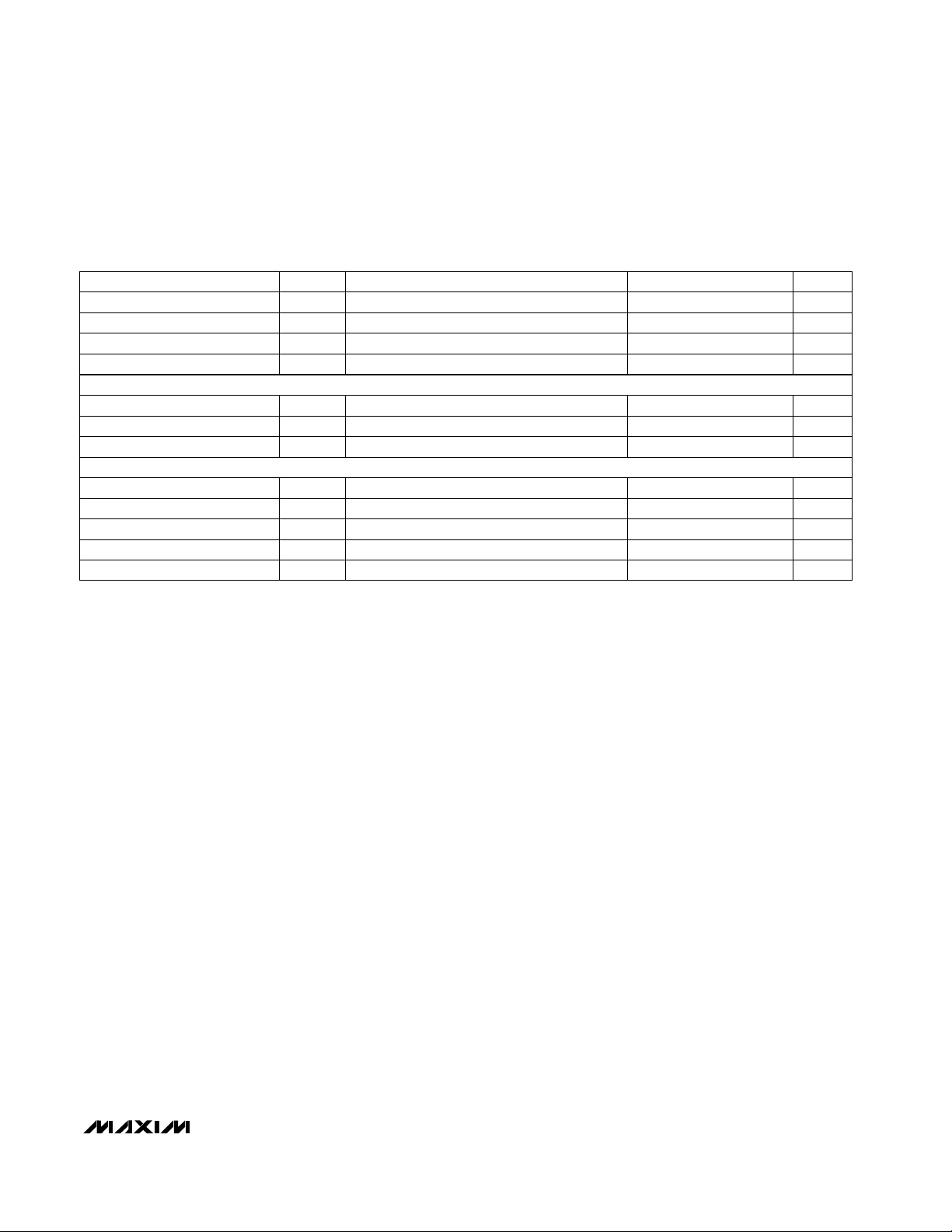
ELECTRICAL CHARACTERISTICS (continued)
(VDD= +2.7V to +5.5V, RL= 10kΩ, CL= 100pF, TA= T
MIN
to T
MAX
, unless otherwise noted. Typical values are at VDD= +3V and
T
A
= +25°C.)
Note 1: Reduced digital code range (code 00 hex to code F0 hex) due to swing limitations when the output amplifier is loaded.
Note 2: Gain error is: [100 (V
F0,meas
- ZCE - V
F0,ideal
) / VDD]. Where V
F0,meas
is the DAC output voltage with input code F0 hex, and
V
F0,ideal
is the ideal DAC output voltage with input code F0 hex (i.e., VDD· 240 / 256).
Note 3: Output settling time is measured from the 50% point of the falling edge of WR to ±1/2LSB of V
OUT
’s final value.
Note 4: Channel-to-Channel Isolation is defined as the glitch energy at a DAC output in response to a full-scale step change on any
other DAC output. The measured channel has a fixed code of 80 hex.
Note 5: Digital Feedthrough is defined as the glitch energy at any DAC output in response to a full-scale step change on all eight
data inputs with WR at V
DD
.
Note 6: R
L
= ∞ , digital inputs at GND or VDD.
Note 7: Timing measurement reference level is (V
IH
+ VIL) / 2.
CONDITIONS UNITSMIN TYP MAXSYMBOLPARAMETER
Digital-to-Analog Glitch Impulse Code 80 hex to code 7F hex 90 nVs
Wideband Amplifier Noise 60 µV
RMS
Shutdown Recovery Time t
SDR
To ±1/2LSB of final value of V
OUT
13 µs
Time to Shutdown t
SDN
IDD< 5µA 20 µs
Power-Supply Voltage V
DD
2.7 5.5 V
Supply Current (Note 6) I
DD
280 520 µA
Shutdown Current 13µA
Address to WR Setup
t
AS
5 ns
Address to WR Hold
t
AH
0 ns
Data to WR Setup
t
DS
25 ns
WR Pulse Width
t
WR
20 ns
Data to WR Hold
t
DH
0 ns
POWER SUPPLIES
DIGITAL TIMING (Figure 1) (Note 7)
 Loading...