General Description
The MAX5099 offers a dual-output, high-switching-frequency DC-DC buck converter with an integrated highside switch. The MAX5099 integrates two low-side
MOSFET drivers to allow each converter to drive an
external synchronous-rectifier MOSFET. Converter 1
delivers up to 2A output current, and converter 2 can
deliver up to 1A of output current. The MAX5099 integrates load-dump protection circuitry that is capable of
handling load-dump transients up to 80V for automotive
applications. The load-dump protection circuit utilizes
an internal charge pump to drive the gate of an external
n-channel MOSFET. When an overvoltage or loaddump condition occurs, the series protection MOSFET
absorbs the high voltage transient to prevent damage
to lower voltage components.
The DC-DC converter operates over a wide 4.5V to 19V
operating voltage range. The MAX5099 operates 180°
out-of-phase with an adjustable switching frequency to
minimize external components while allowing the ability
to make trade-offs between the size, efficiency, and
cost. The high switching frequency also allows these
devices to operate outside the AM band for automotive
applications. These regulators can be protected
against high voltage transients such as a load-dump
condition by using the integrated overvoltage controller.
This device utilizes voltage-mode control for stable
operation and external compensation, so that the loop
gain is tailored to optimize component selection and
transient response. The MAX5099 has a maximum duty
cycle of 92.5% and is synchronized to an external clock
fed at the SYNC input.
Additional features include internal digital soft-start,
individual enable for each DC-DC regulator (EN1 and
EN2), open-drain power-good outputs (PGOOD1 and
PGOOD2), and shutdown input (ON/OFF).
Other features of the MAX5099 include overvoltage protection and short-circuit (hiccup current limit) and thermal protection. The MAX5099 is available in a thermally
enhanced, exposed pad 5mm x 5mm, 32-pin TQFN
package and operates over the automotive -40°C to
+125°C temperature range.
Applications
Automotive AM/FM Radio Power Supply
Automotive Instrument Cluster Display
Features
♦ Wide 4.5V to 5.5V or 5.2V to 19V Input Voltage
Range with 80V Load-Dump Protection
♦ Dual-Output DC-DC Converter with Integrated
Power MOSFETs
♦ Adjustable Outputs from 0.8V to 0.9V
IN
♦ Output Current Capability Up to 2A and 1A
♦ Switching Frequency Programmable from 200kHz
to 2.2MHz
♦ Synchronization Input (SYNC)
♦ Individual Converter Enable Input and Power-
Good Output
♦ Low-I
Q
(7µA) Standby Current (ON/OFF)
♦ Internal Digital Soft-Start and Soft-Stop
♦ Short-Circuit Protection on Outputs and
Maximum Duty-Cycle Limit
♦ Overvoltage Protection on Outputs with Auto
Restart
♦ Thermal Shutdown
♦ Thermally Enhanced 32-Pin TQFN Package
Dissipates Up to 2.7W at +70°C
MAX5099
Dual, 2.2MHz, Automotive Synchronous Buck
Converter with 80V Load-Dump Protection
________________________________________________________________
Maxim Integrated Products
1
Ordering Information
19-4112; Rev 0; 5/08
For pricing, delivery, and ordering information, please contact Maxim Direct at 1-888-629-4642,
or visit Maxim’s website at www.maxim-ic.com.
Pin Configuration appears at end of data sheet.
EVALUATION KIT
AVAILABLE
+
Denotes a lead-free package.
*
EP = Exposed pad.
PART TEMP RANGE PIN-PACKAGE
MAX5099ATJ+
-40°C to +125°C
32 TQFN-EP*

MAX5099
Dual, 2.2MHz, Automotive Synchronous Buck
Converter with 80V Load-Dump Protection
2 _______________________________________________________________________________________
ABSOLUTE MAXIMUM RATINGS
ELECTRICAL CHARACTERISTICS
(VDRV = VL, V+ = VL= IN_HIGH = 5.2V or V+ = IN_HIGH = 5.2V to 19V, EN_ = VL, SYNC = GND, IVL= 0mA, PGND = SGND,
C
BYPASS
= 0.22μF (low ESR), CVL= 4.7μF (ceramic), CV+= 1μF (low ESR), C
IN_HIGH
= 1μF (ceramic), R
IN_HIGH
= 3.9kΩ, R
OSC
= 10kΩ,
T
J
= -40°C to +125°C, unless otherwise noted.) (Note 2)
Stresses beyond those listed under “Absolute Maximum Ratings” may cause permanent damage to the device. These are stress ratings only, and functional
operation of the device at these or any other conditions beyond those indicated in the operational sections of the specifications is not implied. Exposure to
absolute maximum rating conditions for extended periods may affect device reliability.
Note 1: Package thermal resistances were obtained using the method described in JEDEC specifications. For detailed information
on package thermal considerations refer to www.maxim-ic.com/thermal-tutorial
.
V+ to SGND............................................................-0.3V to +25V
V+ to IN_HIGH...........................................................-19V to +6V
IN_HIGH to SGND ..................................................-0.3V to +19V
IN_HIGH Maximum Input Current .......................................60mA
BYPASS to SGND..................................................-0.3V to +2.5V
GATE to V+.............................................................-0.3V to +12V
GATE to SGND .......................................................-0.3V to +36V
SGND to PGND .....................................................-0.3V to +0.3V
V
L
to SGND..................-0.3V to the Lower of +6V or (V+ + 0.3V)
VDRV to SGND .........................................................-0.3V to +6V
BST1/VDD1, BST2/VDD2, DRAIN_,
PGOOD_ to SGND ..............................................-0.3V to +30V
ON/OFF to SGND ...............................-0.3V to (IN_HIGH + 0.3V)
BST1/VDD1 to SOURCE1,
BST2/VDD2 to SOURCE2......................................-0.3V to +6V
SOURCE_ to SGND................................................-0.6V to +25V
EN_ to SGND............................................................-0.3V to +6V
OSC, FSEL_1, COMP_, SYNC,
FB_ to SGND..............................................-0.3V to (V
L
+ 0.3V)
DL_ to PGND ...........................................-0.3V to (VDRV + 0.3V)
SOURCE1, DRAIN1 Peak Current ..............................5A for 1ms
SOURCE2, DRAIN2 Peak Current ..............................3A for 1ms
V
L
, BYPASS to
SGND Short Circuit ................... Continuous, Internally Limited
Continuous Power Dissipation (T
A
= +70°C)
32-Pin TQFN-EP (derate 34.5mW/°C above +70°C)..2759mW
Package Junction-to-Ambient
Thermal Resistance (θ
JA
) (Note 1).............................29.0°C/W
Package Junction-to-Case
Thermal Resistance (θ
JC
) (Note 1) ..............................1.7°C/W
Operating Temperature Range .........................-40°C to +125°C
Storage Temperature Range ............................-65°C to +150°C
Junction Temperature......................................................+150°C
Lead Temperature (soldering, 10s) ................................+300°C
PARAMETER SYMBOL CONDITIONS MIN TYP MAX UNITS
SYSTEM SPECIFICATIONS
V+ = IN_HIGH 5.2 19
Input Voltage Range V+
V
L
= V+ = IN_HIGH, Figure 6 (Note 3) 4.5 5.5
V
V+ Operating Supply Current I
Q
VL unloaded, no switching, V
FB_
= 1V 4.2 6.0 mA
V+ Standby Supply Current I
V+STBY
V
EN_
= 0V, PGOOD_ unconnected,
V+ = V
IN_HIGH
= 14V
0.75 1.1 mA
V+ = VL = 5.2V 86
V+ = 12V 85
Efficiency η
V
OUT1
= 5V at 1.5A,
V
OUT2
= 3.3V at 0.75A,
f
SW
= 300kHz
V+ = 16V 85
%
OVERVOLTAGE PROTECTOR
IN_HIGH Clamp Voltage IN_HIGH I
SINK
= 10mA 19 20 21 V
IN_HIGH Clamp Load
Regulation
1mA < I
SINK
< 50mA 160 mV
IN_HIGH Supply Current I
IN_HIGH
V
EN_
= V
PGOOD_
= V
GATE
= 0V,
V
IN_HIGH
= V
ON/OFF
= 14V
270 600 μA
IN_HIGH Standby Supply
Current
I
IN_HIGHSTBY
V
ON/OFF
= 0V , V
PGOOD_
= V + =
unconnected, V
IN_HIGH
= 14V
79μA
V+ to IN_HIGH Overvoltage
Clamp
V
OV
VOV = V+ - V
IN_HIGH
, I
GATE
= -1mA 1.20 1.85 2.50 V

MAX5099
Dual, 2.2MHz, Automotive Synchronous Buck
Converter with 80V Load-Dump Protection
_______________________________________________________________________________________ 3
PARAMETER SYMBOL CONDITIONS MIN TYP MAX UNITS
Rising, ON/OFF = IN_HIGH, GATE rising 3.6 4.1
IN_HIGH Startup Voltage
IN_HIGH
UVLO
Falling, ON/OFF = IN_HIGH, GATE falling 3.45
V
GATE Charge Current I
GATE_CH
V
IN_HIGH
= V
ON/OFF
= 14V,
V
GATE
= V+ = 0V
20 45 80 μA
V+ = V
IN_HIGH
= V
ON/OFF
= 4.5V,
I
GATE
= 1μA
4.0 5.3 7.5
GATE Output Voltage
V
GATE
-
V
IN_HIGH
V+ = V
IN_HIGH
= V
ON/OFF
= 14V,
I
GATE
= 1μA
9
V
GATE Turn-Off Pulldown
Current
I
GATE_PD
V
IN_HIGH
= 14V, V
ON/OFF
= 0V, V+ = 0V,
V
GATE
= 5V
3.6 mA
STARTUP/VL REGULATOR
VL Undervoltage-Lockout Trip
Level
UVLO V
L
falling 3.9 4.1 4.3 V
VL Undervoltage-Lockout
Hysteresis
180 mV
VL Output Voltage V
L
I
SOURCE_
= 0 to 40mA, 5.5V ≤ V+ ≤ 19V 5.0 5.2 5.5 V
VL LDO Short-Circuit Current I
VL_SHORT
V+ = V
IN_HIGH
= 5.2V 130 mA
VL LDO Dropout Voltage V
LDO
I
SOURCE_
= 40mA, V+ = V
IN_HIGH
= 4.5V 300 550 mV
BYPASS OUTPUT
BYPASS Voltage V
BYPASSIBYPASS
= 0μA 1.98 2.00 2.02 V
BYPASS Load Regulation ΔV
BYPASS
0 < I
BYPASS
< 100μA (sourcing) 2 5 mV
SOFT-START/SOFT-STOP
Digital Ramp Period SoftStart/Soft-Stop
Internal 6-bit DAC 2048
f
SW
Clock
Cycles
Soft-Start/Soft-Stop Steps 64 Steps
VOLTAGE-ERROR AMPLIFIER
FB_ Input Bias Current I
FB_
250 nA
-40°C ≤ TA ≤ +85°C 0.783 0.8 0.809
FB_ Input-Voltage Set Point V
FB_
-40°C ≤ TA ≤ +125°C 0.785 0.814
V
FB_ to COMP_
Transconductance
g
M
1.4 2.4 3.4 mS
INTERNAL MOSFETS
I
SWITCH
= 100mA, BST1/VDD1 to
V
SOURCE1
= 5.2V
195
On-Resistance High-Side
MOSFET Converter 1
R
ON1
I
SWITCH
= 100mA, BST1/VDD1 to
V
SOURCE1
= 4.5V
208 355
mΩ
ELECTRICAL CHARACTERISTICS (continued)
(VDRV = VL, V+ = VL= IN_HIGH = 5.2V or V+ = IN_HIGH = 5.2V to 19V, EN_ = VL, SYNC = GND, IVL= 0mA, PGND = SGND,
C
BYPASS
= 0.22μF (low ESR), CVL= 4.7μF (ceramic), CV+= 1μF (low ESR), C
IN_HIGH
= 1μF (ceramic), R
IN_HIGH
= 3.9kΩ, R
OSC
= 10kΩ,
T
J
= -40°C to +125°C, unless otherwise noted.) (Note 2)

MAX5099
Dual, 2.2MHz, Automotive Synchronous Buck
Converter with 80V Load-Dump Protection
4 _______________________________________________________________________________________
ELECTRICAL CHARACTERISTICS (continued)
(VDRV = VL, V+ = VL= IN_HIGH = 5.2V or V+ = IN_HIGH = 5.2V to 19V, EN_ = VL, SYNC = GND, IVL= 0mA, PGND = SGND,
C
BYPASS
= 0.22μF (low ESR), CVL= 4.7μF (ceramic), CV+= 1μF (low ESR), C
IN_HIGH
= 1μF (ceramic), R
IN_HIGH
= 3.9kΩ, R
OSC
= 10kΩ,
T
J
= -40°C to +125°C, unless otherwise noted.) (Note 2)
PARAMETER SYMBOL CONDITIONS MIN TYP MAX UNITS
I
SWITCH
= 100mA, BST2/VDD2 to
V
SOURCE2
= 5.2V
280
On-Resistance High-Side
MOSFET Converter 2
R
ON2
I
SWITCH
= 100mA, BST2/VDD2 to
V
SOURCE2
= 4.5V
300 520
mΩ
Minimum Converter 1 Output
Current
I
OUT1
V
OUT1
= 5V, V+ = 12V (Note 4) 2 A
Minimum Converter 2 Output
Current
I
OUT2
V
OUT2
= 3.3V, V+ = 12V (Note 4) 1 A
Converter 1/Converter 2
MOSFET DRAIN_ Leakage
Current
I
LK12
V
EN1
= V
EN2
= 0V, VDS = 19V, V
DRAIN_
=
19V, V
SOURCE_
= 0V
20 μA
Internal Weak Low-Side Switch
On-Resistance
R
ONLSSW_ILSSW
= 30mA 22 Ω
INTERNAL SWITCH CURRENT LIMIT
Internal Switch Current-Limit
Converter 1
I
CL1
V+ = V
IN_HIGH
= 5.2V, VL = VDRV =
V
BST_/VDD_
= 5.2V
2.8 3.45 4.3 A
Internal Switch Current-Limit
Converter 2
I
CL2
V+ = V
IN_HIGH
= 5.2V, VL = VDRV =
V
BST_/VDD_
= 5.2V
1.75 2.10 2.60 A
SWITCHING FREQUENCY
PWM Maximum Duty Cycle D
MAX
SYNC = SGND, fSW = 1.25MHz 90 92 100 %
Switching Frequency Range f
SW
200 2200 kHz
Switching Frequency f
SW
R
OSC
= 6.81kΩ, each converter 1.7 1.9 2.1 MHz
5.6kΩ < R
OSC
< 10kΩ, 1% 5
Switching Frequency Accuracy
10kΩ < R
OSC
< 62.5kΩ, 1% 7
%
SYNC Frequency Range f
SYNC
Each converter switching frequency is half
of the SYNC input frequency,
FSEL_1 = V
L
(see the Setting the
Switching Frequency section)
400 4400 kHz
SYNC High Threshold V
SYNCH
2V
SYNC Low Threshold V
SYNCL
0.8 V
SYNC Input Leakage I
SYNC_LEAK
2μA
SYNC Input Minimum Pulse
Width
t
SYNCIN
100 ns
Sync to Source 1 Phase Delay SYNC
PHASEROSC
= 62.5kΩ 90 Degrees

MAX5099
Dual, 2.2MHz, Automotive Synchronous Buck
Converter with 80V Load-Dump Protection
_______________________________________________________________________________________ 5
ELECTRICAL CHARACTERISTICS (continued)
(VDRV = VL, V+ = VL= IN_HIGH = 5.2V or V+ = IN_HIGH = 5.2V to 19V, EN_ = VL, SYNC = GND, IVL= 0mA, PGND = SGND,
C
BYPASS
= 0.22μF (low ESR), CVL= 4.7μF (ceramic), CV+= 1μF (low ESR), C
IN_HIGH
= 1μF (ceramic), R
IN_HIGH
= 3.9kΩ, R
OSC
= 10kΩ,
T
J
= -40°C to +125°C, unless otherwise noted.) (Note 2)
PARAMETER SYMBOL CONDITIONS MIN TYP MAX UNITS
INTERNAL DL_ DRIVERS
R
DS(ON)
DL_ Sink R
ONDLN
I
SINK
= 200mA
1
Ω
R
DS(ON)
DL_ Source R
ONDLP
I
SOURCE
= 200mA
1.8
Ω
Break-Before-Make Time 50
ns
FSEL_1
FSEL_1 Input High Threshold V
IH
2V
FSEL_1 Input Low Threshold V
IL
0.8 V
FSEL_1 Input Leakage I
FSEL_1_LEAK
2μA
ON/OFF
ON/OFF Input High Threshold V
IH
2V
ON/OFF Input Low Threshold V
IL
0.8 V
ON/OFF Input Leakage Current I
ON/OFF_LEAKVON/OFF
= 5V 0.35 2 μA
EN_ INPUTS
EN_ Input High Threshold V
IH
EN_ rising 1.9 2.0 2.1 V
EN_ Input Hysteresis V
EN_HYS
0.5 V
EN_ Input Leakage Current I
EN_LEAK
-1 +1 μA
POWER-GOOD OUTPUT (PGOOD1, PGOOD2)
PGOOD_ Threshold V
TPGOOD_
Falling 90 92.5 95 % V
FB_
PGOOD_ Output Voltage V
PGOOD_ISINK
= 3mA 0.4 V
PGOOD_ Output Leakage
Current
I
LKPGOOD_
V+ = VL = V
IN_HIGH
= V
EN_
= 5.2V,
V
PGOOD_
= 23V, V
FB_
= 1V
2μA
OUTPUT OVERVOLTAGE PROTECTION
FB_ OVP Threshold Rising V
OVP_R
107 114 121 % V
FB
FB_ OVP Threshold Falling V
OVP_F
112.5 % V
FB
THERMAL PROTECTION
Thermal Shutdown T
SHDN
Rising +165 °C
Thermal Hysteresis T
HYST
20 °C
Note 2: 100% tested at TA= +25°C and TA= +125°C. Specifications at TA= -40°C are guaranteed by design and not production
tested.
Note 3: Operating supply range (V+) is guaranteed by V
L
line regulation test. Connect V+ to IN_HIGH and VLfor 5V operation.
Note 4: Output current is limited by the power dissipation of the package; see the
Power Dissipation
section in the
Applications
Information
section.

MAX5099
Dual, 2.2MHz, Automotive Synchronous Buck
Converter with 80V Load-Dump Protection
6 _______________________________________________________________________________________
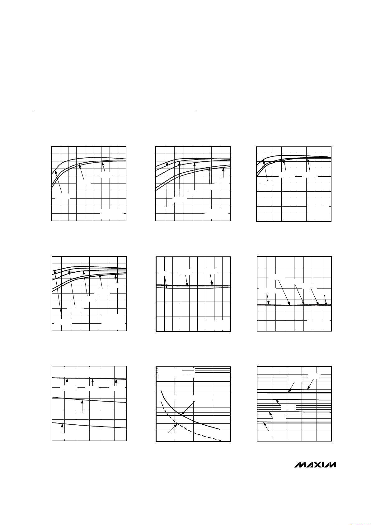
Typical Operating Characteristics
(V+ = V
IN_HIGH
= 14V, unless otherwise noted. V+ = V
IN_HIGH
means that N1 is shorted externally.)
OUTPUT1 EFFICIENCY
vs. LOAD CURRENT
MAX5099 toc01
LOAD CURRENT (A)
OUTPUT1 EFFICIENCY (%)
1.81.61.2 1.40.6 0.8 1.00.4
10
20
30
40
50
60
70
80
90
100
0
0.2 2.0
VIN = 8V
VIN = 14V
VIN = 16V
V
OUT
= 5V
f
SW
= 1.85MHz
OUTPUT2 EFFICIENCY
vs. LOAD CURRENT
MAX5099 toc02
LOAD CURRENT (A)
OUTPUT2 EFFICIENCY (%)
0.90.7 0.80.4 0.5 0.60.3
10
20
30
40
50
60
70
80
90
100
0
0.2 1.0
VIN = 4.5V
VIN = 5.5V
V
OUT
= 3.3V
f
SW
= 1.85MHz
VIN = 14V
VIN = 8V
VIN = 16V
OUTPUT1 EFFICIENCY
vs. LOAD CURRENT
MAX5099 toc03
LOAD CURRENT (A)
OUTPUT1 EFFICIENCY (%)
1.81.61.2 1.40.6 0.8 1.00.4
10
20
30
40
50
60
70
80
90
100
0
0.2 2.0
VIN = 8V
VIN = 14V VIN = 16V
V
OUT
= 5V
f
SW
= 300kHz
L1 = 18μH
OUTPUT2 EFFICIENCY
vs. LOAD CURRENT
MAX5099 toc04
LOAD CURRENT (A)
OUTPUT2 EFFICIENCY (%)
0.90.80.6 0.70.4 0.50.30.2 1.0
10
20
30
40
50
60
70
80
90
100
0
VIN = 16V
VIN = 8V
VIN = 14V
VIN = 5.5V
VIN = 4.5V
V
OUT
= 3.3V
f
SW
= 300kHz
L2 = 27μH
OUTPUT1 VOLTAGE
vs. LOAD CURRENT
MAX5099 toc05
LOAD CURRENT (A)
OUTPUT1 VOLTAGE (V)
1.81.61.41.21.00.80.60.4
4.92
4.94
4.96
4.98
5.00
4.90
0.2 2.0
VIN = 8V
VIN = 14V
VIN = 16V
V
OUT
= 5V
f
SW
= 1.85MHz
OUTPUT2 VOLTAGE
vs. LOAD CURRENT
MAX5099 toc06
LOAD CURRENT (A)
OUTPUT2 VOLTAGE (V)
0.90.80.70.60.50.40.3
3.25
3.24
3.26
3.27
3.28
3.29
3.30
3.23
0.2 1.0
VIN = 4.5V
VIN = 16V
VIN = 14V
VIN = 8V
VIN = 5.5V
V
OUT
= 3.3V
f
SW
= 1.85MHz
VL OUTPUT VOLTAGE
vs. CONVERTER SWITCHING FREQUENCY
MAX5099 toc07
CONVERTER SWITCHING FREQUENCY (kHz)
V
L
OUTPUT VOLTAGE (V)
1600 19001300700 1000
4.2
4.4
4.6
4.8
5.0
5.2
5.4
4.0
400 2200
VIN = 4.5V
VIN = 5.5V
VIN = 8V
VIN = 19V
VIN = 5V
BOTH CONVERTERS SWITCHING
FSEL_1 = V
L
EACH CONVERTER SWITCHING
FREQUENCY vs. R
OSC
MAX5099 toc08
R
OSC
(kΩ)
SWITCHING FREQUENCY (MHz)
604020
1
0
80
10
0.1
CONVERTER 1, CONVERTER 2
CONVERTER 1
FSEL_1 = VL,
FSEL_1 = GND,
EACH CONVERTER SWITCHING
FREQUENCY vs. TEMPERATURE
MAX5099 toc09
TEMPERATURE (°C)
SWITCHING FREQUENCY (MHz)
-5 30 65 100
1
10
0.1
-40 135
0.3MHz
0.6MHz
1.25MHz
1.85MHz
2.2MHz
FSEL_1 = V
L

MAX5099
Dual, 2.2MHz, Automotive Synchronous Buck
Converter with 80V Load-Dump Protection
_______________________________________________________________________________________
7
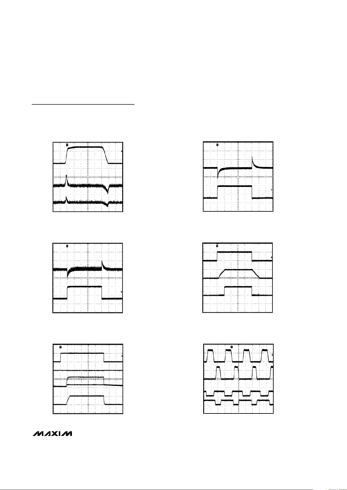
LINE-TRANSIENT RESPONSE
(BUCK CONVERTER)
MAX5099 toc10
0V
1ms/div
V
IN
5V/div
V
OUT1
= 5.0V/1.5A
AC-COUPLED
200mV/div
V
OUT2
= 3.3V/0.75A
AC-COUPLED
200mV/div
0V
CONVERTER 1
LOAD-TRANSIENT RESPONSE
MAX5099 toc11
100μs/div
V
OUT1
= 5.0V
AC-COUPLED
200mV/div
I
OUT1
1A/div
0A
CONVERTER 2
LOAD-TRANSIENT RESPONSE
MAX5099 toc12
100μs/div
V
OUT2
= 3.3V
AC-COUPLED
200mV/div
I
OUT2
500mA/div
0A
SOFT-START/SOFT-STOP FROM EN1
MAX5099 toc13
1ms/div
V
OUT1
= 5V/2A
5V/div
EN1
5V/div
P
GOOD1
5V/div
0V
0V
0V
fSW = 1.85MHz
SOFT-START FROM ON/OFF
MAX5099 toc14
2ms/div
V
OUT1
= 5V/2A
5V/div
ON/OFF
5V/div
GATE
10V/div
V+
10V/div
V
L
= EN1 = EN2
5V/div
0V
0V
0V
0V
OUT-OF-PHASE OPERATION
(FSEL_1 = V
L
)
MAX5099 toc15
200ns/div
SOURCE2
10V/div
DL1
10V/div
DL2
10V/div
SOURCE1
10V/div
0V
0V
0V
0V
Typical Operating Characteristics (continued)
(V+ = V
IN_HIGH
= 14V, unless otherwise noted. V+ = V
IN_HIGH
means that N1 is shorted externally.)

MAX5099
Dual, 2.2MHz, Automotive Synchronous Buck
Converter with 80V Load-Dump Protection
8 _______________________________________________________________________________________
Typical Operating Characteristics (continued)
(V+ = V
IN_HIGH
= 14V, unless otherwise noted. V+ = V
IN_HIGH
means that N1 is shorted externally.)
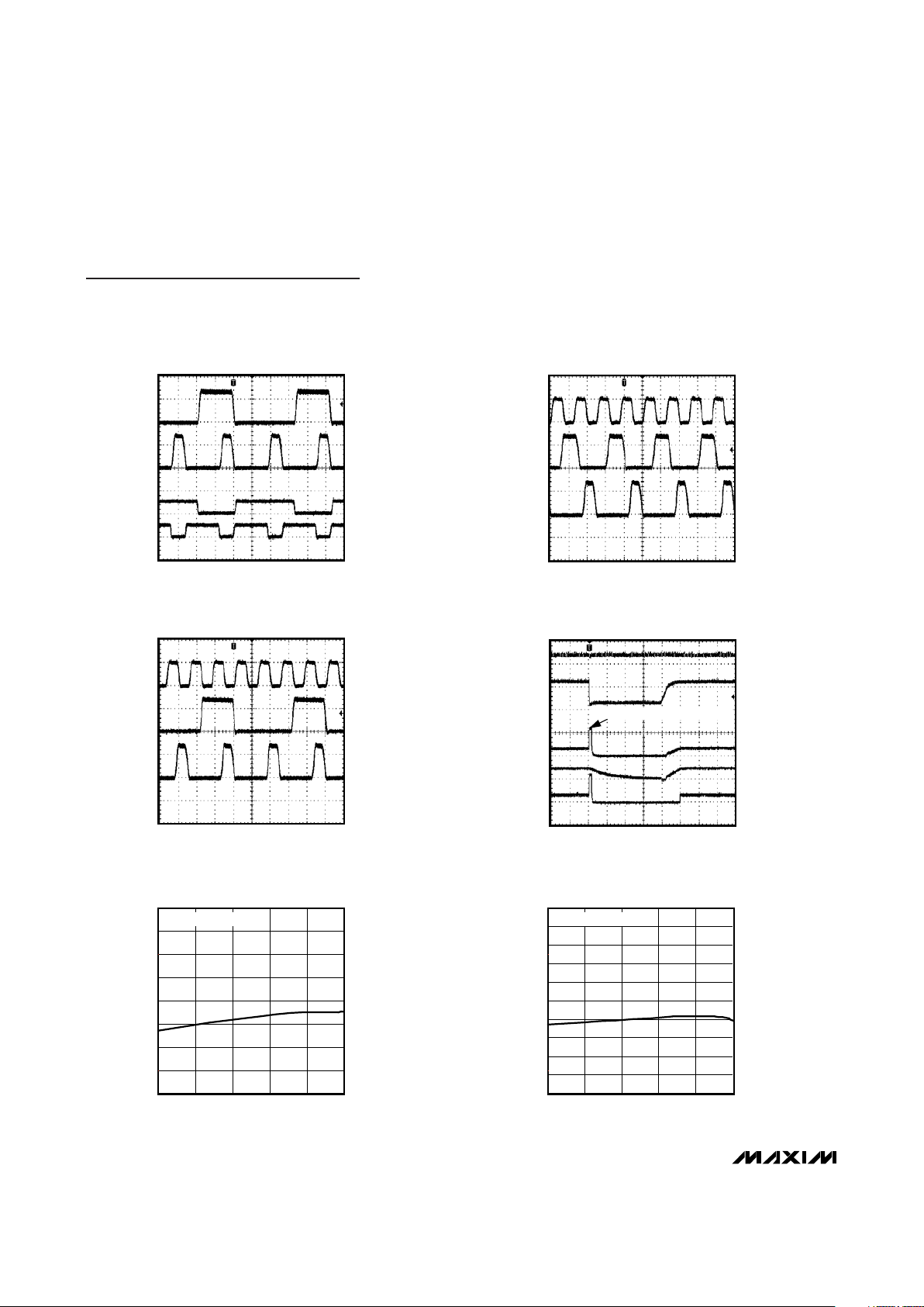
FB_ VOLTAGE
vs. TEMPERATURE
MAX5099 toc20
TEMPERATURE (°C)
FB_ VOLTAGE (V)
10065-5 30
0.790
0.795
0.800
0.805
0.815
0.810
0.820
0.825
0.785
-40 135
VL = V+ = V
IN_HIGH
= 5.5V
BYPASS VOLTAGE
vs. TEMPERATURE
MAX5099 toc21
TEMPERATURE (°C)
BYPASS VOLTAGE (V)
10065-5 30
1.994
1.996
1.998
2.000
2.002
2.006
2.004
2.008
2.010
1.990
1.992
-40 135
VL = V+ = V
IN_HIGH
= 5.5V
EXTERNAL SYNCHRONIZATION
(FSEL_1 = SGND )
MAX5099 toc18
200ns/div
SOURCE2
10V/div
SOURCE1
10V/div
0V
SYNC
5V/div
0V
0V
OVP BEHAVIOR
MAX5099 toc19
1ms/div
PGOOD2
10V/div
VOUT1
10V/div
VOUT2
10V/div
GATE
10V/div
0V
0V
0V
V+
10V/div
0V
0V
EXTERNAL OVERVOLTAGE REMOVED
OUT-OF-PHASE OPERATION
(FSEL_1 = SGND)
MAX5099 toc16
200ns/div
SOURCE2
10V/div
DL1
10V/div
DL2
10V/div
SOURCE1
10V/div
0V
0V
0V
0V
EXTERNAL SYNCHRONIZATION
(FSEL_1 = V
L
)
MAX5099 toc17
200ns/div
SOURCE2
10V/div
SOURCE1
10V/div
0V
SYNC
5V/div
0V
0V

MAX5099
Dual, 2.2MHz, Automotive Synchronous Buck
Converter with 80V Load-Dump Protection
_______________________________________________________________________________________
9
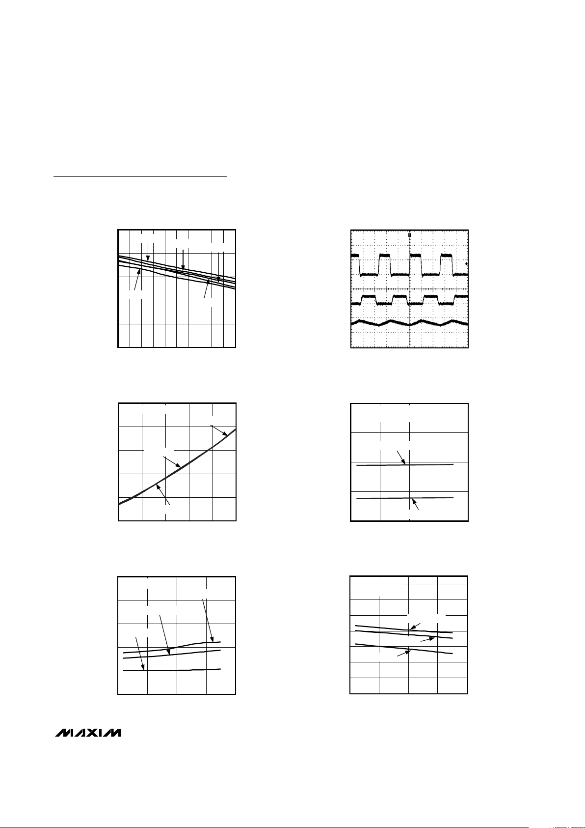
BYPASS VOLTAGE
vs. BYPASS CURRENT
MAX5099 toc22
BYPASS CURRENT (μA)
BYPASS VOLTAGE (V)
806020 40
1.992
1.994
1.998
1.996
2.000
1.990
0100705010 30 90
TA = +25°C
TA = +135°C
TA = +125°C
TA = +85°C
TA = -40°C
SOURCE1, I
SOURCE1
, DL1, I
IDL1
MAX5099 toc23
200ns/div
I
SOURCE1
1A/div
SOURCE1
10V/div
DL1
10V/div
OV
0V
0A
V+ SWITCHING SUPPLY CURRENT
vs. SWITCHING FREQUENCY
MAX5099 toc24
SWITCHING FREQUENCY (kHz)
V+ SWITCHING SUPPLY CURRENT (mA)
182014401060680
20
40
60
80
100
0
300 2200
TA = +25°C
TA = +135°C
TA = -40°C
V+ = IN_HIGH = ON/OFF
V+ STANDBY SUPPLY CURRENT
vs. TEMPERATURE
MAX5099 toc25
TEMPERATURE (°C)
V+ STANDBY SUPPLY CURRENT (mA)
100500
1
2
3
4
0
-50 150
fSW = 1.85MHz
fSW = 300kHz
V+ = IN_HIGH = ON/OFF
EN1 = EN2 = SGND
IN_HIGH SHUTDOWN CURRENT
vs. TEMPERATURE
MAX5099 toc26
TEMPERATURE (°C)
IN_HIGH SHUTDOWN CURRENT (μA)
100500
4
8
12
16
20
0
-50 150
IN_HIGH = 8V
IN_HIGH = 14V
IN_HIGH = 16V
ON/OFF = SGND
IN_HIGH STANDBY CURRENT
vs. TEMPERATURE
MAX5099 toc27
TEMPERATURE (°C)
IN_HIGH STANDBY CURRENT (μA)
100500
85
95
105
115
125
135
145
75
-50 150
IN_HIGH = 8V
IN_HIGH = 14V
IN_HIGH = 16V
ON/OFF = IN_HIGH
EN1 = EN2 = SGND
Typical Operating Characteristics (continued)
(V+ = V
IN_HIGH
= 14V, unless otherwise noted. V+ = V
IN_HIGH
means that N1 is shorted externally.)
 Loading...