

Page 1
现货库存、技术资料、百科信息、热点资讯,精彩尽在鼎好!
General Description
The MAX5060/MAX5061 pulse-width modulation (PWM)
DC-DC controllers provide high-output-current capability
in a compact package with a minimum number of external components. These devices utilize an average-current-mode control that enables optimal use of low
R
DS(ON)
MOSFETs, eliminating the need for external
heatsinks even when delivering high output currents.
Differential sensing (MAX5060) enables accurate control
of the output voltage, while adaptive voltage positioning
provides optimum transient response. An internal regulator enables operation with 4.75V to 5.5V or 7V to 28V
input voltage ranges. The high switching frequency, up
to 1.5MHz, allows the use of low-output inductor values
and input capacitor values. This accommodates the use
of PC-board-embedded planar magnetics.
The MAX5060 features a clock output with 180° phase
delay to control a second out-of-phase converter for
lower capacitor ripple currents. The MAX5060 also limits
the reverse current if the bus voltage becomes higher
than the regulated output voltage. The MAX5060 is
specifically designed to limit current sinking when multiple power-supply modules are paralleled. The
MAX5060/MAX5061 offer an adjustable 0.6V to 5.5V output voltage. The MAX5060 offers an overvoltage protection, power-good signal, and an output enable function.
The MAX5060/MAX5061 operate over the automotive
temperature range (-40°C to +125°C). The MAX5060 is
available in a 28-pin thin QFN package while the
MAX5061 is available in a 16-pin TSSOP package.
Applications
Servers and Workstations
Point-of-Load Telecom DC-DC Regulators
Networking Systems
RAID Systems
High-End Desktop Computers
Features
♦ 4.75V to 5.5V or 7V to 28V Input Voltage Range
♦ Adjustable Output Voltage from 0.6V to 5.5V
♦ Up to 30A Output Current
♦ Can Parallel Outputs For Higher Output Current
♦ Programmable Adaptive Output Voltage
Positioning
♦ True-Differential Remote Output Sensing
(MAX5060)
♦ Average-Current-Mode Control
• Superior Current Sharing Between Paralleled
Modules
• Accurate Current Limit Eliminates MOSFET
and Inductor Derating
♦ Limits Reverse Current Sinking in Paralleled
Modules (MAX5060)
♦ Programmable Switching Frequency from 125kHz
to 1.5MHz
♦ Integrated 4A Gate Drivers
♦ Clock Output for 180° Out-of-Phase Operation
(MAX5060)
♦ Voltage Signal Proportional to Output Current for
Load Monitoring (MAX5060)
♦ Output Overvoltage Crowbar Protection
(MAX5060)
♦ Programmable Hiccup Current-Limit Threshold
and Response Time
♦ Overtemperature Thermal Shutdown
MAX5060/MAX5061
0.6V to 5.5V Output, Parallelable,
Average-Current-Mode DC-DC Controllers
________________________________________________________________ Maxim Integrated Products 1
Ordering Information
Selector Guide
PART TEMP RANGE
PKG
CODE
MAX5060ATI
28 TQFN-EP*
T2855-3
MAX5060ETI
28 TQFN-EP*
T2855-3
MAX5061AUE
U16E-3
MAX5061EUE
U16E-3
PART OUTPUT
MAX5060
Average-Current-Mode DC-DC Controller
for 5V/12V/24V Input Bus with CLKOUT,
Load Monitoring, Overvoltage, EN Input,
SYNC Input, and PGOOD Output
MAX5061
Average-Current-Mode DC-DC Controller
for 5V/12V/24V Input with SYNC/ENABLE
Input
19-3583; Rev 2; 7/05
For pricing, delivery, and ordering information, please contact Maxim/Dallas Direct! at
1-888-629-4642, or visit Maxim’s website at www.maxim-ic.com.
Pin Configurations appear at end of data sheet.
*EP = Exposed pad.
-40°C to +125°C
-40°C to +85°C
-40°C to +125°C 16 TSSOP-EP*
-40°C to +85°C 16 TSSOP-EP*
PIN-PACKAGE
Page 2
MAX5060/MAX5061
0.6V to 5.5V Output, Parallelable,
Average-Current-Mode DC-DC Controllers
2 _______________________________________________________________________________________
ABSOLUTE MAXIMUM RATINGS
Stresses beyond those listed under “Absolute Maximum Ratings” may cause permanent damage to the device. These are stress ratings only, and functional
operation of the device at these or any other conditions beyond those indicated in the operational sections of the specifications is not implied. Exposure to
absolute maximum rating conditions for extended periods may affect device reliability.
IN to SGND.............................................................-0.3V to +30V
BST to SGND..........................................................-0.3V to +35V
DH to LX .......................................-0.3V to [(V
BST
- V
LX_
) + 0.3V]
DL to PGND (MAX5060).............................-0.3V to (V
DD
+ 0.3V)
DL to PGND (MAX5061).............................-0.3V to (V
CC
+ 0.3V)
BST to LX..................................................................-0.3V to +6V
V
CC
to SGND............................................................-0.3V to +6V
V
CC
, VDDto PGND ...................................................-0.3V to +6V
SGND to PGND .....................................................-0.3V to +0.3V
Current Sink in PGOOD ........................................................6mA
All Other Pins to SGND...............................-0.3V to (V
CC
+ 0.3V)
Continuous Power Dissipation (T
A
= +70°C)
16-Pin TSSOP (derate 21.3mW/°C above +70°C)* ......1702mW
28-Pin TQFN (derate 34.5mW/°C above +70°C)*......2758mW
Operating Temperature Range
MAX5060A_ _ and MAX5061A_ _ .................-40°C to +125°C
MAX5060E_ _ and MAX5061E_ _....................-40°C to +85°C
Maximum Junction Temperature .....................................+150°C
Storage Temperature Range .............................-60°C to +150°C
Lead Temperature (soldering, 10s) .................................+300°C
*Per JEDEC 51 standard.
ELECTRICAL CHARACTERISTICS
(VCC= 5V, VDD= VCC(MAX5060 only), TA= TJ= T
MIN
to T
MAX
, unless otherwise noted. Typical specifications are at TA= +25°C.)
(Note 1)
PARAMETER SYMBOL CONDITIONS
MIN
TYP
MAX
UNITS
SYSTEM SPECIFICATIONS
728
Input Voltage Range V
IN
Short IN and VCC together for 5V input
operation
V
Quiescent Supply Current I
Q
EN = VCC or SGND, not switching 2.7 5.5 mA
Efficiency η I
LOAD
= 20A, VIN = 12V, V
OUT
= 3.3V 90 %
OUTPUT VOLTAGE
No load, VCC = 4.75V to 5.5V,
f
SW
= 500kHz
0.6
SENSE+ to SENSE- Accuracy
(MAX5060) (Note 2)
0.6
V
Soft-Start Time t
SS
Clock
Cycles
No load, VCC = 4.75V to 5.5V,
no switching
0.6
EAN Reference Voltage
(MAX5061)
V
REF
0.6
V
STARTUP/INTERNAL REGULATOR
VCC Undervoltage Lockout UVLO VCC rising 4.1 4.3 4.5 V
VCC Undervoltage Lockout
Hysteresis
mV
VCC Output Voltage
5.1
V
MOSFET DRIVERS
Output-Driver Impedance R
ON
Low or high output,
I
SOURCE/SINK
= 20mA
1.1 3 Ω
Output-Driver Source/Sink Current
I
DH_
, I
DL_
4A
Nonoverlap Time t
NO
C
DH/DL
= 5nF 35 ns
4.75 5.50
No load, VIN = 7V to 28V, fSW = 500kHz 0.594
No load, VIN = 7V to 28V, no switching 0.591
VIN = 7V to 28V, I
= 0 to 60mA 4.85
SOURCE
0.594
1024
0.591
200
0.606
0.606
0.606
0.606
5.30
Page 3
MAX5060/MAX5061
0.6V to 5.5V Output, Parallelable,
Average-Current-Mode DC-DC Controllers
_______________________________________________________________________________________ 3
ELECTRICAL CHARACTERISTICS (continued)
(VCC= 5V, VDD= VCC(MAX5060 only), TA= TJ= T
MIN
to T
MAX
, unless otherwise noted. Typical specifications are at TA= +25°C.)
(Note 1)
PARAMETER SYMBOL CONDITIONS
MIN
TYP
MAX
UNITS
OSCILLATOR
Switching Frequency Range 125
kHz
RT = 500kΩ 121
RT = 120kΩ 495
Switching Frequency f
SW
RT = 39.9kΩ
kHz
120kΩ ≤ RT ≤ 500kΩ -5 +5
Switching Frequency Accuracy
40kΩ ≤ R
T
≤ 120kΩ -8 +8
%
CLKOUT Phase Shift (MAX5060)
φ
CLKOUT
fSW = 125kHz
degrees
CLKOUT Output Low Level
(MAX5060)
V
CLKOUTLISINK
= 2mA 0.4 V
CLKOUT Output High Level
(MAX5060)
V
CLKOUTHISOURCE
= 2mA 4.5 V
SYNC Input-High Pulse Width t
SYNC
RT/SYNC (MAX5060), RT/SYNC/EN
(MAX5061)
200 ns
SYNC Input Clock High Threshold
V
SYNCH
RT/SYNC (MAX5060), RT/SYNC/EN
(MAX5061)
2.0 V
SYNC Input Clock Low Threshold
V
SYNCL
RT/SYNC (MAX5060), RT/SYNC/EN
(MAX5061)
0.4 V
SYNC Pullup Current I
SYNC_OUT
V
RT/SYNC
= 0V (MAX5060),
V
RT/SYNC/EN
= 0V (MAX5061)
µA
SYNC Power-Off Level V
SYNC_OFF
0.4 V
CURRENT LIMIT
Average Current-Limit Threshold
V
CL
CSP to CSN
mV
Reverse Current-Limit Threshold V
CLR
CSP to CSN (MAX5060)
mV
Cycle-by-Cycle Current Limit CSP to CSN 60 mV
Cycle-by-Cycle Overload
Response Time
V
CSP
to V
CSN
= 75mV
ns
Hiccup Divider Ratio LIM to VCM, no switching
V/V
Hiccup Reset Delay
ms
LIM Input Impedance LIM to SGND
kΩ
CURRENT-SENSE AMPLIFIER
CSP to CSN Input Resistance R
CS
4kΩ
Common-Mode Range V
CMR(CS)
VIN = 7V to 28V 0 5.5 V
Input Offset Voltage V
OS(CS)
0.1 mV
Amplifier Gain A
V(CS)
V/V
3dB Bandwidth f
3dB
4
MHz
1515 1620 1725
24.0 26.9 28.2
-3.2 -2.3 -0.1
0.547 0.558 0.565
125 129
521 547
180
250 750
260
200
55.9
34.5
1500
Page 4
MAX5060/MAX5061
0.6V to 5.5V Output, Parallelable,
Average-Current-Mode DC-DC Controllers
4 _______________________________________________________________________________________
ELECTRICAL CHARACTERISTICS (continued)
(VCC= 5V, VDD= VCC(MAX5060 only), TA= TJ= T
MIN
to T
MAX
, unless otherwise noted. Typical specifications are at TA= +25°C.)
(Note 1)
PARAMETER SYMBOL CONDITIONS
MIN
TYP
MAX
UNITS
CURRENT-ERROR AMPLIFIER (Transconductance Amplifier)
Transconductance g
C
µS
Open-Loop Gain A
VOL(CE)
No load 50 dB
DIFFERENTIAL VOLTAGE AMPLIFIER (DIFF, MAX5060 only)
Common-Mode Voltage Range V
CMR(DIFF)
0
V
DIFF Output Voltage V
CM
V
SENSE+
= V
SENSE-
= 0V 0.6 V
Input Offset Voltage V
OS(DIFF)
-1 +1 mV
Amplifier Gain A
V(DIFF)
1
V/V
3dB Bandwidth f
3dB
C
DIFF
= 20pF 3
MHz
Minimum Output-Current Drive I
OUT(DIFF)
4mA
SENSE+ to SENSE- Input
Resistance
R
VS
V
SENSE-
= 0V 50
kΩ
V_IOUT AMPLIFIER (V_IOUT, MAX5060 only)
Gain-Bandwidth Product V
V_IOUT
= 2.0V 4
MHz
3dB Bandwidth V
V_IOUT
= 2.0V 1.0
MHz
Output Sink Current 30 µA
Output Source Current 90 µA
Maximum Load Capacitance 50 pF
V_IOUT Output to I
OUT
Transfer
Function
R
SENSE
= 1mΩ,
100mV ≤ V_IOUT ≤ 5.5V
mV/A
Offset Voltage 1mV
VOLTAGE-ERROR AMPLIFIER (EAOUT)
Open-Loop Gain A
VOLEA
70 dB
Unity-Gain Bandwidth f
GBW
3
MHz
V
EAN
= 2.0V (MAX5060)
EAN Input Bias Current I
B(EA)
V
EAN
= 0.4V, V
EAOUT
= GND
(MAX5061)
µA
Error-Amplifier Output-Clamping
Voltage
V
CLAMP(EA)
With respect to VCM (MAX5060),
with respect to SGND (MAX5061)
883
mV
POWER-GOOD AND OVERVOLTAGE PROTECTION (MAX5060 only)
PGOOD Trip Level V
UV
PGOOD goes low when V
OUT
is below
this threshold
90
%V
OUT
PGOOD Output Low Level V
PGLO
I
SINK
= 4mA 0.4 V
PGOOD Output Leakage Current
I
PG
PGOOD = V
CC
1µA
OVI Trip Threshold OVP
TH
With respect to SGND
V
OVI Input Bias Current I
OVI
0.2 µA
550
+1.0
0.994
1.006
100
132.3 135 137.7
-0.2 0.03 +0.2
930 976
87.5
1.244 1.276 1.308
92.5
Page 5
MAX5060/MAX5061
0.6V to 5.5V Output, Parallelable,
Average-Current-Mode DC-DC Controllers
_______________________________________________________________________________________ 5
ELECTRICAL CHARACTERISTICS (continued)
(VCC= 5V, VDD= VCC(MAX5060 only), TA= TJ= T
MIN
to T
MAX
, unless otherwise noted. Typical specifications are at TA= +25°C.)
(Note 1)
PARAMETER SYMBOL CONDITIONS
MIN
TYP
MAX
UNITS
ENABLE INPUTS
EN Input High Voltage (MAX5060)
V
EN
EN rising
2.5
V
EN Input Hysteresis (MAX5060)
V
EN Pullup Current (MAX5060) I
EN
15
µA
RT/SYNC/EN Input High Voltage
Enable (MAX5061)
1.6 V
RT/SYNC/EN Input Low Voltage
Disable (MAX5061)
0.4 V
THERMAL SHUTDOWN
Thermal Shutdown Temperature rising
°C
Thermal-Shutdown Hysteresis 30 °C
Note 1: Specifications at TA= +25°C are 100% tested. Specifications over the temperature range are guaranteed by design.
Note 2: Does not include an error due to finite error amplifier gain (see the Voltage-Error Amplifier section).
V
RT/SYNC/EN_H
V
RT/SYNC/EN_L
2.437
0.28
13.5
+150
2.562
16.5
Page 6
EFFICIENCY vs. OUTPUT CURRENT
AND INPUT VOLTAGE
MAX5060 toc01
OUTPUT CURRENT (A)
η (%)
181612 144 6 8 102
10
20
30
40
50
60
70
80
90
100
0
020
V
OUT
= 3.3V
f
SW
= 250kHz
VIN = 5V
VIN = 12V
EFFICIENCY vs. OUTPUT CURRENT
AND INPUT VOLTAGE
MAX5060 toc02
OUTPUT CURRENT (A)
η (%)
181612 144 6 8 102
10
20
30
40
50
60
70
80
90
100
0
020
V
OUT
= 0.6V
f
SW
= 250kHz
VIN = 5V
VIN = 12V
EFFICIENCY vs. OUTPUT CURRENT
MAX5060 toc03
OUTPUT CURRENT (A)
η (%)
181612 144 6 8 102
10
20
30
40
50
60
70
80
90
100
0
020
VIN = 24V
V
OUT
= 3.3V
f
SW
= 125kHz
EFFICIENCY vs. OUTPUT CURRENT
AND OUTPUT VOLTAGE
MAX5060 toc04
OUTPUT CURRENT (A)
η (%)
181612 144 6 8 102
10
20
30
40
50
60
70
80
90
100
0
020
VIN = 12V
f
SW
= 250kHz
V
OUT
= 5V
V
OUT
= 3.3V
V
OUT
= 0.6V
V
OUT
= 1V
V
OUT
= 1.8V
EFFICIENCY vs. OUTPUT CURRENT
AND OUTPUT VOLTAGE
MAX5060 toc05
OUTPUT CURRENT (A)
η (%)
181612 144 6 8 102
10
20
30
40
50
60
70
80
90
100
0
020
VIN = 5V
f
SW
= 500kHz
V
OUT
= 3.3V
V
OUT
= 1.8V
V
OUT
= 1V
V
OUT
= 0.6V
SUPPLY CURRENT (IQ) vs. FREQUENCY
MAX5060 toc06
FREQUENCY (kHz)
SUPPLY CURRENT (mA)
13001100900700500300
10
20
30
40
50
60
0
100 1500
EXTERNAL CLOCK
NO DRIVER LOAD
VIN = 12V
VIN = 24V
VIN = 5V
SUPPLY CURRENT vs. TEMPERATURE
MAX5060 toc07
TEMPERATURE (°C)
SUPPLY CURRENT (mA)
603510-15
62
64
66
68
70
60
-40 85
VIN = 12V
f
SW
= 250kHz
C
DL/CDH
= 22nF
CURRENT-SENSE THRESHOLD
vs. OUTPUT VOLTAGE
MAX5060 toc08
V
OUT
(V)
(V
CSP
- V
CSN
) (mV)
4321
26.5
27.0
27.5
28.0
28.5
29.0
26.0
05
VIN = 12V
f
SW
= 250kHz
HICCUP CURRENT LIMIT vs. R
EXT
MAX5060 toc09
R
EXT
(MΩ)
CURRENT LIMIT (A)
161284
23.5
24.0
24.5
25.0
25.5
26.0
23.0
020
VIN = 12V
f
SW
= 250kHz
R1 = 1mΩ
V
OUT
= 1.5V
MAX5060/MAX5061
0.6V to 5.5V Output, Parallelable,
Average-Current-Mode DC-DC Controllers
6 _______________________________________________________________________________________
Typical Operating Characteristics
(TA = +25°C, Figures 1 and 2, unless otherwise noted.)
Page 7
LOW-SIDE DRIVER (DL) SINK
AND SOURCE CURRENT
MAX5060 toc16
3A/div
100ns/div
C
LOAD
= 22nF
V
IN
= 12V
Typical Operating Characteristics (continued)
(TA = +25°C, Figures 1 and 2, unless otherwise noted.)
OUTPUT VOLTAGE vs. OUTPUT CURRENT
AND ERROR AMPLIFIER GAIN (R
F/RIN
)
MAX5060 toc10
OUTPUT CURRENT (A)
OUTPUT VOLTAGE (V)
181612 144 6 8 102
1.325
1.350
1.375
1.400
1.425
1.450
1.475
1.500
1.525
1.550
1.575
1.600
1.300
020
VIN = 12V
f
SW
= 250kHz
V
OUT
= 1.5V
RF/RIN = 40
RF/RIN = 10
RF/RIN = 20
V_IOUT VOLTAGE vs. LOAD CURRENT
MAX5060 toc11
LOAD CURRENT (A)
V
V_IOUT
(V)
15105
0.5
1.0
1.5
2.0
2.5
3.0
0
020
V
OUT
= 3.3V
R1 = 1m
Ω
MAX5060
VIN = 12V
VIN = 7V
VIN = 24V
VCC LOAD REGULATION
vs. INPUT VOLTAGE
MAX5060 toc12
VCC LOAD CURRENT (mA)
V
CC
(V)
125100755025
4.85
4.95
5.05
5.15
5.25
4.75
0150
VIN = 12V
VIN = 5V
VIN = 24V
DRIVER RISE TIME
vs. DRIVER LOAD CAPACITANCE
MAX5060 toc13
CAPACITANCE (nF)
t
R
(ns)
2116116
20
40
60
80
100
0
1
VIN = 12V
f
SW
= 250kHz
DH
DL
DRIVER FALL TIME
vs. DRIVER LOAD CAPACITANCE
MAX5060 toc14
CAPACITANCE (nF)
t
F
(ns)
2116116
20
40
60
80
100
0
1
VIN = 12V
f
SW
= 250kHz
DH
DL
HIGH-SIDE DRIVER (DH) SINK
AND SOURCE CURRENT
MAX5060 toc15
2A/div
100ns/div
C
LOAD
= 22nF
V
IN
= 12V
HIGH-SIDE DRIVER (DH) RISE TIME
MAX5060 toc17
2V/div
40ns/div
C
LOAD
= 22nF
V
IN
= 12V
HIGH-SIDE DRIVER (DH) FALL TIME
MAX5060 toc18
2V/div
40ns/div
C
LOAD
= 22nF
V
IN
= 12V
MAX5060/MAX5061
0.6V to 5.5V Output, Parallelable,
Average-Current-Mode DC-DC Controllers
_______________________________________________________________________________________ 7
Page 8
REVERSE CURRENT SINK
vs. TEMPERATURE
MAX5060 toc25
TEMPERATURE (°C)
SINK CURRENT (A)
603510-15
1.6
1.8
2.0
2.2
2.4
1.4
-40
VIN = 12V
V
0UT
= 1.5V
R1 = 1m
Ω
V
EXTERNAL
= 3.3V
V
EXTERNAL
= 2V
85
LOW-SIDE DRIVER (DL) RISE TIME
MAX5060 toc19
2V/div
40ns/div
C
LOAD
= 22nF
V
IN
= 12V
LOW-SIDE DRIVER (DL) FALL TIME
MAX5060 toc20
2V/div
40ns/div
C
LOAD
= 22nF
V
IN
= 12V
OUTPUT RIPPLE
MAX5060 toc21
50mV/div
1µs/div
VIN = 12V
V
OUT
= 1.5V
I
OUT
= 20A
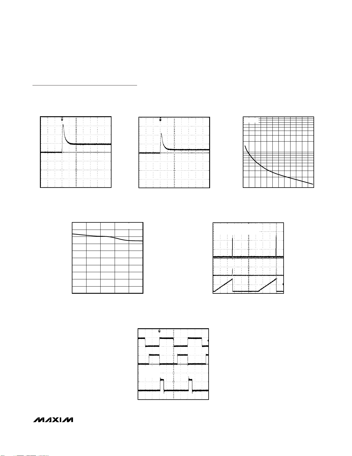
INPUT STARTUP RESPONSE
MAX5060 toc22
V
OUT
2V/div
2ms/div
VIN = 12V
V
OUT
= 1.5V
I
OUT
= 20A
V
PGOOD
5V/div
V
IN
5V/div
ENABLE STARTUP RESPONSE
MAX5060 toc23
V
OUT
2V/div
2ms/div
VIN = 12V
V
OUT
= 1.5V
I
OUT
= 20A
V
PGOOD
5V/div
V
EN
2V/div
LOAD-TRANSIENT RESPONSE
MAX5060 toc24
100µs/div
VIN = 12V
V
OUT
= 3.3V
I
STEP
= 5A TO 20A
SLEW = 2A/µs
V
OUT
200mV/div
I
OUT
10A/div
0
REVERSE CURRENT SINK AT INPUT TURN-ON
(V
IN
= 12V, V
OUT
= 1.5V, V
EXTERNAL
= 2.0V)
MAX5060 toc26
200µs/div
2A/div
REVERSE CURRENT SINK AT INPUT TURN-ON
(V
IN
= 12V, V
OUT
= 1.5V, V
EXTERNAL
= 3.3V)
MAX5060 toc27
200µs/div
5A/div
Typical Operating Characteristics (continued)
(TA = +25°C, Figures 1 and 2, unless otherwise noted.)
MAX5060/MAX5061
0.6V to 5.5V Output, Parallelable,
Average-Current-Mode DC-DC Controllers
8 _______________________________________________________________________________________
Page 9
Typical Operating Characteristics (continued)
(TA = +25°C, Figures 1 and 2, unless otherwise noted.)
REVERSE CURRENT SINK AT ENABLE TURN-ON
(V
IN
= 12V, V
OUT
= 1.5V, V
EXTERNAL
= 2.0V)
MAX5060 toc28
200µs/div
2A/div
REVERSE CURRENT SINK AT ENABLE TURN-ON
(V
IN
= 12V, V
OUT
= 1.5V, V
EXTERNAL
= 3.3V)
MAX5060 toc29
200µs/div
5A/div
FREQUENCY vs. R
T
MAX5060 toc30
RT (kΩ)
f
SW
(kHz)
470
430
390
350
310
270
230
190
150
110
70
1000
10,000
100
30 510
VIN = 12V
FREQUENCY vs. TEMPERATURE
MAX5060 toc31
TEMPERATURE (°C)
f
SW
(kHz)
603510-15
242
244
246
248
250
252
254
256
258
260
240
-40 85
VIN = 12V
OUTPUT SHORT-CIRCUIT WAVEFORM
MAX5060 toc32
40ms/div
V
OUT
2V/div
V
IN
= 12V CEN = 0.47µF
V
OUT
= 3.3V R
LIM
= OPEN
EN
2V/div
I
OUT
10A/div
SYNC, CLKOUT, AND LX WAVEFORM
MAX5060 toc33
1µs/div
CLKOUT
5V/div
VIN = 12V
f
SW
= 250kHz
LX
10V/div
SYNC
5V/div
MAX5060/MAX5061
0.6V to 5.5V Output, Parallelable,
Average-Current-Mode DC-DC Controllers
_______________________________________________________________________________________ 9
Page 10
MAX5060/MAX5061
0.6V to 5.5V Output, Parallelable,
Average-Current-Mode DC-DC Controllers
10 ______________________________________________________________________________________
Pin Description
PIN
MAX5060 MAX5061
1 3 PGND
2, 7 8 N.C. No Connection. Not internally connected.
3 4 DL Low-Side Gate-Driver Output. Synchronous MOSFET gate driver.
4 5 BST
NAME FUNCTION
Power Ground. Connect PGND, low-side synchronous MOSFET’s source, and
(MAX5060)/VCC (MAX5061) bypass capacitor returns together.
V
DD
Boost Flying-Capacitor Connection. Reservoir capacitor connection for the highside MOSFET driver supply. Connect a 0.47µF ceramic capacitor between BST
and LX.
56 LX
6 7 DH High-Side Gate-Driver Output. Drives the gate of the high-side MOSFET.
8, 22, 25 16 SGND
9 — CLKOUT
10 — PGOOD
11 — EN
12 — RT/SYNC
13 — V_IOUT
14 10 LIM
15 — OVI
Inductor Connection. Source connection for the high-side MOSFETs. Also serves
as the return terminal for the high-side driver.
Signal Ground. Ground connection for the internal control circuitry. Connect
SGND and PGND together at one point near the input bypass capacitor return.
Oscillator Output. Rising edge of CLKOUT is phase-shifted from rising edge of
DH by 180°.
Power-Good Output. PGOOD is an open-drain output that goes low when the
programmed output voltage falls out of regulation. The power-good comparator
threshold is 90% of the programmed output voltage.
Output Enable. Drive EN high or leave unconnected for normal operation. Drive
EN low to shut down the power drivers. EN has an internal 15µA pullup current.
Connect a capacitor from EN to SGND to program the hiccup mode duty cycle.
Switching Frequency Programming and Chip-Enable Input. Connect a resistor
from RT/SYNC to SGND to set the internal oscillator frequency. Drive RT/SYNC
externally to synchronize the switching frequency with system clock.
Voltage-Source Output Proportional to the Output Load Current. The voltage at
V_IOUT is 135 x I
Current-Limit Setting Input. Connect a resistor from LIM to SGND to set the
hiccup current-limit threshold. Connect a capacitor from LIM to SGND to ignore
short output overcurrent pulses.
Overvoltage Protection Circuit Input. Connect OVI to DIFF. When OVI exceeds
+12.7% above the programmed output voltage, DH is latched low and DL is
latched high. Toggle EN low to high or recycle the power to reset the latch.
LOAD
x RS.
16 11 CLP
Current-Error-Amplifier Output. Compensate the current loop by connecting an
RC network to ground.
Page 11

MAX5060/MAX5061
0.6V to 5.5V Output, Parallelable,
Average-Current-Mode DC-DC Controllers
______________________________________________________________________________________ 11
Pin Description (continued)
PIN
MAX5060 MAX5061
17 12 EAOUT
18 13 EAN
19 — DIFF
20 14 CSN
21 15 CSP
23 — SENSE-
24 — SENSE+
26 1 IN Supply Voltage Connection. Connect IN to VCC for a +5V system.
27 2 V
NAME FUNCTION
Voltage-Error-Amplifier Output. Connect to the external gain-setting feedback
resistor. The error-amplifier gain-setting resistors determine the amount of
adaptive voltage positioning.
Voltage-Error-Amplifier Inverting Input. Receives a signal from the output of the
differential remote-sense amplifier (MAX5060). Connect the center tap of the
resistor-divider from the output to SGND (MAX5061).
Differential Remote-Sense Amplifier Output. DIFF is the output of a precision
unity-gain amplifier whose inputs are SENSE+ and SENSE-.
Current-Sense Differential Amplifier Negative Input. The differential voltage
between CSN and CSP is amplified internally by the current-sense amplifier
(gain = 34.5) to measure the inductor current.
Current-Sense Differential Amplifier Positive Input. The differential voltage
between CSP and CSN is amplified internally by the current-sense amplifier
(gain = 34.5) to measure the inductor current.
Differential Output-Voltage-Sensing Negative Input. SENSE- is used to sense a
CC
remote load. Connect SENSE- to V
Differential Output-Voltage-Sensing Positive Input. SENSE+ is used to sense a
remote load. Connect SENSE+ to V
difference between SENSE+ and SENSE- according to the preset reference
voltage of 0.6V.
Internal +5V Regulator Output. VCC is derived from the IN voltage. Bypass V
to SGND with 4.7µF and 0.1µF ceramic capacitors. For MAX5061, connect an
additional 0.1µF bypass capacitor from V
or PGND at the load.
OUT-
at the load. The device regulates the
OUT+
to PGND.
CC
CC
Supply Voltage for Low-Side and High-Side Drivers. Connect a parallel
28 — V
— 9 RT/SYNC/EN
—— EP
DD
combination of 0.1µF and 1µF ceramic capacitors to PGND and a 1Ω resistor to
V
CC
Switching Frequency Programming and Chip-Enable Input. Connect a resistor
from RT/SYNC/EN to SGND to set the internal oscillator frequency. Drive
RT/SYNC/EN externally to synchronize the switching frequency with system
clock. If RT/SYNC/EN is held low for 50µs, the device turns off the output drivers.
Exposed Paddle. Connect the exposed paddle to a copper pad (SGND) to
improve power dissipation.
to filter out the high peak currents of the driver from the internal circuitry.
Page 12

MAX5060/MAX5061
0.6V to 5.5V Output, Parallelable,
Average-Current-Mode DC-DC Controllers
12 ______________________________________________________________________________________
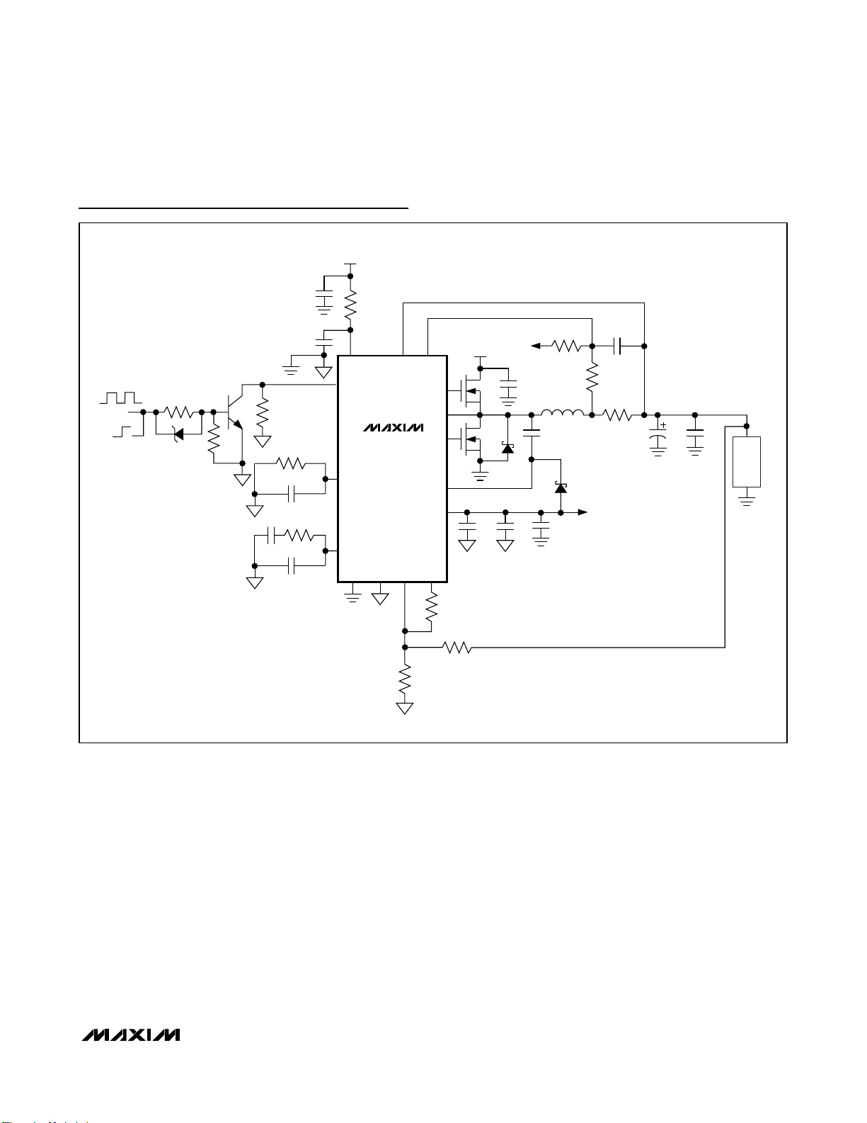
Typical Application Circuit
Figure 1. Typical Application Circuit, VIN= 12V (MAX5060)
VIN = 12V
C1, C2
C3
R
EXT
C4
ON
OFF
(VOLTAGE α I
V_IOUT
OUT
C5
)
R
IN
R
F
R13
IN
IN
SENSE- SENSE+
LIM
EN
CSN
MAX5060
V_IOUT
OVI
DIFF
EAN
EAOUT
PGNDCLP SGND
R5
C6
C7
PGOOD
CSP
RT/
SYNC
V
V
DH
BST
R
H
V
IN
R
C3–C7
Q1
LX
DL
CC
DD
Q2
D1
R3
C8
L1 R1
C12
D3
SYNC
R11
C10
C12 C13
C11
L
LOAD
V
= 0.6V TO
OUT
5.5V AT 20A
PGOOD
Page 13
MAX5060/MAX5061
0.6V to 5.5V Output, Parallelable,
Average-Current-Mode DC-DC Controllers
______________________________________________________________________________________ 13
Typical Application Circuit (continued)
Figure 2. Typical Application Circuit, VIN= +12V (MAX5061)
SYNC
ON
OFF
VIN = 12V
C1, C2
C3
R
T
R
EXT
C4
C5
R5
C6
R13
IN
IN
RT/SYNC/EN
MAX5061
LIM
CLP
PGND SGND
CSN
EAN
CSP
BST
V
EAOUT
CC
C13–C16
RC1
L1 R1
C12
C9
V
V
IN
F
Q1
Q2
C7* C8
D1
DH
LX
DL
CC
R
C13*
RC2
V
= 0.6V TO
OUT
5.5V AT 20A
C10 C11
LOAD
D3
V
CC
R
H
R
L
* USE C13 = 47pf AND C7 = 4.7µF/6.3V (CERAMIC).
Page 14
MAX5060/MAX5061
0.6V to 5.5V Output, Parallelable,
Average-Current-Mode DC-DC Controllers
14 ______________________________________________________________________________________
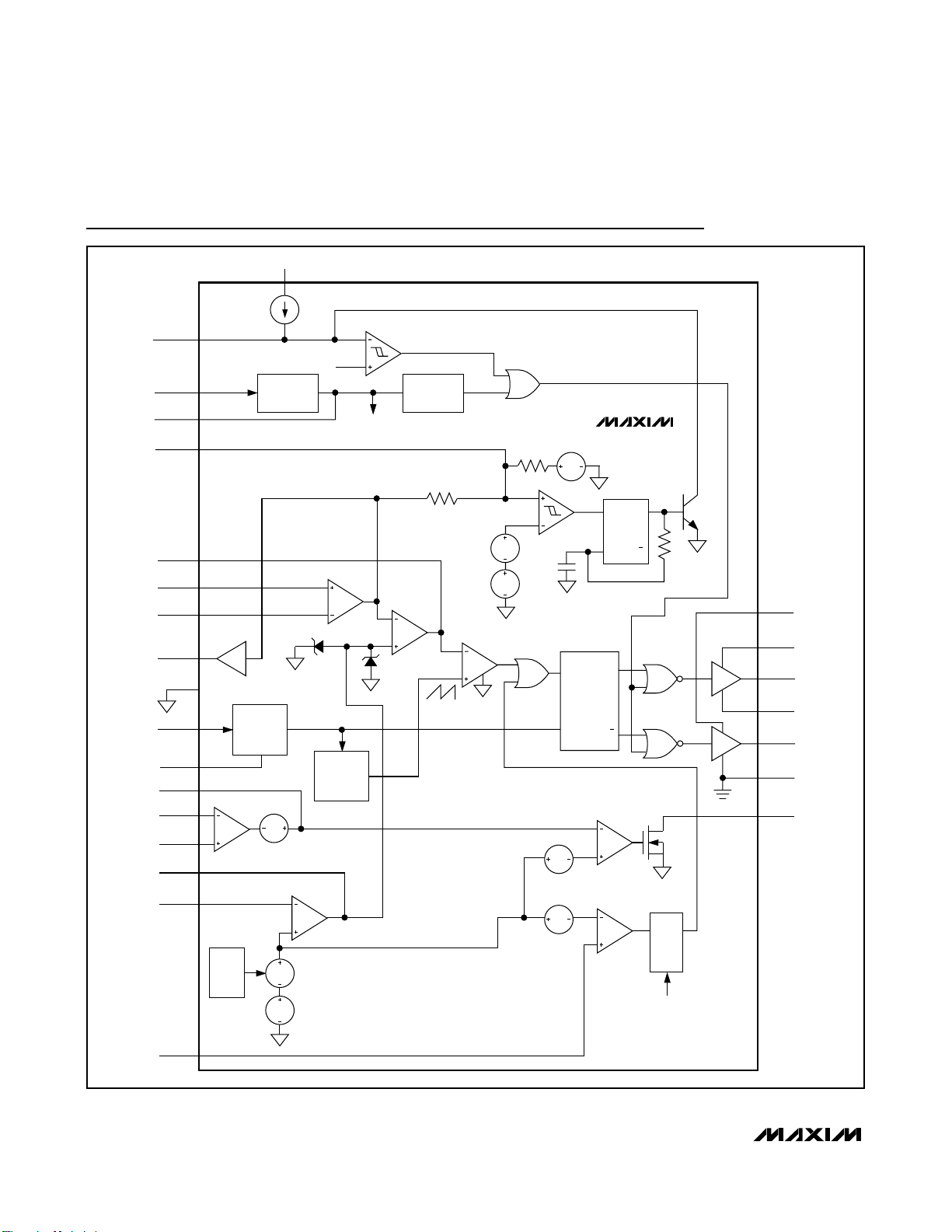
Block Diagram
Figure 3. Functional Diagram (MAX5060)
V
CC
I
S
EN
0.5V x V
CC
gm = 500µS
CEA
V
CLAMP
HIGH
UVLO
POR
TEMP SENSOR
100kΩ
0.5 x V
RAMP
2 x fS (V/s)
HICCUP MODE
CURRENT LIMIT
CLAMP
V
CM
PWM
COMPARATOR
CPWM
126.7kΩ
C
t
0.1 x V
0.12 x V
V
CM
S
R
REF
REF
MAX5060
SRQ
Q
Q
Q
N
OVP LATCH
LATCH
OVP COMP
CLEAR ON UVLO RESET OR
ENABLE LOW
R
T
IN
V
CC
LIM
5V
LDO
REGULATOR
TO INTERNAL
CIRCUITS
CLP
= 34.5
A
V
CLAMP
LOW
GENERATOR
ERROR AMP
VEA
V
= 0.6V
REF
VCM (0.6V)
V
CA
RAMP
CSP
CSN
V_IOUT
SGND
RT/SYNC
CLKOUT
DIFF
SENSE-
SENSE+
EAOUT
EAN
A
= 4
V
DIFF
AMP
SOFTSTART
OSCILLATOR
+0.6V
CLK
V
DD
BST
DH
LX
DL
PGND
PGOOD
OVI
Page 15

MAX5060/MAX5061
0.6V to 5.5V Output, Parallelable,
Average-Current-Mode DC-DC Controllers
______________________________________________________________________________________ 15
Block Diagram (continued)
Figure 4. Functional Diagram (MAX5061)
V
LIM
CLP
CSP
CSN
SGND
RT/SYNC/EN
V
CC
I
S
0.5V x V
CC
TEMP SENSOR
gm = 500µS
CEA
CLAMP
UVLO
POR
100kΩ
0.5 x V
RAMP
2 x fS (V/s)
HICCUP MODE
CURRENT LIMIT
CLAMP
V
CM
PWM
COMPARATOR
CPWM
126.7kΩ
V
CM
C
t
S
R
MAX5061
SRQ
Q
Q
R
T
Q
V
CC
BST
DH
LX
DL
IN
CC
OSCILLATOR
5V
LDO
REGULATOR
TO INTERNAL
= 34.5
A
V
CA
CIRCUITS
CLK
V
HIGH
GENERATOR
EAOUT
EAN
SOFTSTART
ERROR AMP
VEA
V
= 0.6V
REF
RAMP
PGND
Page 16

MAX5060/MAX5061
0.6V to 5.5V Output, Parallelable,
Average-Current-Mode DC-DC Controllers
16 ______________________________________________________________________________________
Detailed Description
The MAX5060/MAX5061 are high-performance averagecurrent-mode PWM controllers. The average-currentmode control technique offers inherently stable
operation, reduces component derating and size by
accurately controlling the inductor current. This also
improves the current-sharing accuracy when paralleling
multiple converters. The devices achieve high efficiency,
at high current (up to 30A) with a minimum number of
external components. The high- and low-side drivers
source and sink up to 4A for lower switching frequencies
while driving high-gate-charge MOSFETs.
The MAX5060’s CLKOUT output is 180° out-of-phase
with respect to the high-side driver. The CLKOUT drives
a second MAX5060 or a MAX5061 regulator out-ofphase, reducing the input capacitor ripple current and
increasing the load current capacity. The paralleling
capability of the MAX5060/MAX5061 improves design
flexibility in applications requiring upgrades (higher load).
The MAX5060/MAX5061 consist of an inner averagecurrent-loop controlled by an outer-voltage-loop voltageerror amplifier (VEA). The combined action of the inner
current loop and outer voltage loop corrects the output
voltage errors by adjusting the inductor current. The
inductor current is sensed across a current-sense resistor. The differential amplifier (MAX5060) senses the output right at the load for true-differential output voltage
sensing. The sensed voltage is compared against internal 0.6V reference at the error-amplifier input. The output
voltage can be set from 0.6V to 5.5V (IN ≥ 7V) using a
resistor-divider at SENSE+ and SENSE-.
IN, VCC, and V
DD
The MAX5060/MAX5061 accept a 4.75V to 5.5V or 7V
to 28V input voltage range. All internal control circuitry
operates from an internally regulated nominal voltage
of 5V (VCC). For input voltages of 7V or greater, the
internal VCCregulator steps the voltage down to 5V.
The VCCoutput voltage is a regulated 5V output capable of sourcing up to 60mA. Bypass the VCCto SGND
with 4.7µF and 0.1µF low-ESR ceramic capacitors for
high-frequency noise rejection and stable operation.
The MAX5060 uses VDDto power the low-side and
high-side drivers, while the MAX5061 uses the VCCto
power internal circuitry as well as the low- and highside driver supply. In the case of the MAX5061, use
one or more 0.1µF low-ESR ceramic capacitors
between VCCand PGND to reject the noise spikes due
to high-current driver switching.
The TQFN-28 and TSSOP-16 are thermally enhanced
packages and can dissipate up to 2.7W and 1.7W,
respectively. The high-power packages allow the
high-frequency, high-current buck converter to operate from a 12V or 24V bus. Calculate power dissipation in the MAX5060/MAX5061 as a product of the
input voltage and the total VCCregulator output current (I
CC
). ICCincludes quiescent current (IQ) and
gate-drive current (IDD):
PD= VINx I
CC
ICC= IQ+ [fSWx (QG1+ QG2)]
where QG1and Q
G2
are the total gate charge of the
low-side and high-side external MOSFETs at V
GATE
=
5V, IQis 3.5mA (typ), and fSWis the switching frequency of the converter.
Undervoltage Lockout (UVLO)
The MAX5060/MAX5061 include an undervoltage lockout with hysteresis and a power-on-reset circuit for converter turn-on and monotonic rise of the output voltage.
The UVLO rising threshold is internally set at 4.35V with
a 200mV hysteresis. Hysteresis at UVLO eliminates
chattering during startup.
Most of the internal circuitry, including the oscillator,
turns on when the input voltage reaches 4V. The
MAX5060/MAX5061 draw up to 3.5mA of current
before the input voltage reaches the UVLO threshold.
Soft-Start
The MAX5060/MAX5061 has an internal digital soft-start
for a monotonic, glitch-free rise of output voltage. Softstart is achieved by the controlled rise of error amplifier
dominant input in steps using a 5-bit counter and a 5-bit
DAC. The soft-start DAC generates a linear ramp from 0
to 0.7V. This voltage is applied to the error amplifier at a
third (noninverting) input. As long as the soft-start voltage is lower than the reference voltage, the system will
converge to that lower reference value. Once the softstart DAC output reaches 0.6V, the reference takes over
and the DAC output continues to climb to 0.7V assuring
that it is out of the way of the reference voltage.
Page 17

MAX5060/MAX5061
0.6V to 5.5V Output, Parallelable,
Average-Current-Mode DC-DC Controllers
______________________________________________________________________________________ 17
Internal Oscillator
The internal oscillator generates a clock with the frequency proportional to the inverse of RT. The oscillator
frequency is adjustable from 125kHz to 1.5MHz with
better than 8% accuracy using a single resistor connected from RT/SYNC to SGND (MAX5060) and from
RT/SYNC/EN to SGND (MAX5061). The frequency accuracy avoids the over-design, size, and cost of passive
filter components like inductors and capacitors. Use the
following equation to calculate the oscillator frequency:
for 120kΩ≤RT≤ 500kΩ:
for 40kΩ≤RT≤ 120kΩ:
The oscillator also generates a 2V
P-P
voltage-ramp signal for the PWM comparator and a 180° out-of-phase
clock signal for CLKOUT (MAX5060) to drive a second
DC-DC converter out-of-phase.
Synchronization
The MAX5060/MAX5061 can be easily synchronized by
connecting an external clock to RT/SYNC (MAX5060) or
RT/SYNC/EN (MAX5061). If an external clock is present, then the internal oscillator is disabled and the
external clock is used to run the MAX5060/MAX5061. If
the external clock is removed, the absence of clock for
32µs is detected and the circuit starts switching from
the internal oscillator. Pulling RT/SYNC on the MAX5060
or RT/SYNC/EN on the MAX5061 to ground for at least
50µs disables the converter.
Use an open-collector transistor to synchronize the
MAX5060/MAX5061 with the external system clock (see
Figures 1 and 2).
Figure 5. MAX5060 Control Loop
R
T
. =×625 10
f
SW
10
R
T
. =×640 10
f
10
SW
C
R
CF
CF
*
R
SENSE+
SENSE-
*R
AND RIN ARE EXTERNAL.
F
DIFF
AMP
IN
C
CSN
CSP
CA
RF*
CEA
VEA
V
+ V
REF
CM
MAX5060
CLP
CPWM
CFF
DRIVE
V
IN
I
L
R
S
C
OUT
V
OUT
LOAD
Page 18

MAX5060/MAX5061
0.6V to 5.5V Output, Parallelable,
Average-Current-Mode DC-DC Controllers
18 ______________________________________________________________________________________
Control Loop
The MAX5060/MAX5061 use an average-current-mode
control scheme to regulate the output voltage (Figure 5).
The main control loop consists of an inner current loop
and an outer voltage loop. The inner loop controls the
output current (I
PHASE
), while the outer loop controls the
output voltage. The inner current loop absorbs the
inductor pole reducing the order of the outer voltage
loop to that of a single-pole system.
The current loop consists of a current-sense resistor
(R
SENSE
), a current-sense amplifier (CA), a currenterror amplifier (CEA), an oscillator providing the carrier
ramp, and a PWM comparator (CPWM) (Figure 6). The
precision CA amplifies the sense voltage across RS by
a factor of 34.5. The inverting input to the CEA senses
the CA output. The CEA output is the difference
between the voltage-error-amplifier output (EAOUT)
and the amplified voltage from the CA. The RC compensation networks connected to CLP provide external
frequency compensation for the CEA. The start of every
clock cycle enables the high-side drivers and initiates a
PWM ON cycle. Comparator CPWM compares the output voltage from the CEA with a 0 to 2V ramp from the
oscillator. The PWM ON cycle terminates when the
ramp voltage exceeds the error voltage.
The MAX5060 outer voltage control loop consists of the
differential amplifier (DIFF AMP), reference voltage, and
VEA. The unity-gain differential amplifier provides truedifferential remote sensing of the output voltage. The differential amplifier output connects to the inverting input
(EAN) of the VEA. For MAX5061, the DIFF AMP is
bypassed and the inverting input is available to the pin
for direct feedback. The noninverting input of the VEA is
internally connected to an internal precision reference
voltage. The MAX5060/MAX5061 reference voltage is set
to 0.6V. The VEA controls the inner current loop (Figure
4). Use a resistive feedback network to set the VEA gain
as required by the adaptive voltage-positioning circuit
(see the Adaptive Voltage Positioning section).
Figure 6. Phase Circuit
PEAK-CURRENT
COMPARATOR
A
CA
60mV
= 34.5
V
gm = 550µS
CEA
COMPARATOR
CLP
CSP
CSN
GM
RAMP
CLK
IN
2 x fS (V/s)
PWM
CPWM
V
DD
MAX5060
BST
S
R
Q
Q
DH
LX
DL
SHDN
PGND
Page 19

MAX5060/MAX5061
0.6V to 5.5V Output, Parallelable,
Average-Current-Mode DC-DC Controllers
______________________________________________________________________________________ 19
Current-Sense Amplifier
The differential current-sense amplifier (CA) provides a
DC gain of 34.5. The maximum input offset voltage of
the current-sense amplifier is 1mV and the commonmode voltage range is 0 to 5.5V (IN = 7V to 28V). The
current-sense amplifier senses the voltage across a
current-sense resistor. The maximum common-mode
voltage is 3.6V when VIN= 5V. The common-mode voltage range determines the maximum output voltage of
the buck converter.
Peak-Current Comparator
The peak-current comparator provides a path for fast
cycle-by-cycle current limit during extreme fault conditions such as an output inductor malfunction (Figure 5).
Note the average current-limit threshold of 26.9mV still
limits the output current during short-circuit conditions.
To prevent inductor saturation, select an output inductor
with a saturation current specification greater than the
average current limit. Proper inductor selection ensures
that only the extreme conditions trip peak-current comparator, such as a broken output inductor. The 60mV
threshold for triggering the peak-current limit is twice the
full-scale average current-limit voltage threshold. The
peak-current comparator has only a 260ns delay.
Current-Error Amplifier
The MAX5060/MAX5061 has a transconductance current-error amplifier (CEA) with a typical gmof 550µS
and 320µA output sink- and source-current capability.
The current-error amplifier output CLP, serves as the
inverting input to the PWM comparator. CLP is externally accessible to provide frequency compensation for
the inner current loops (Figure 5). Compensate (CEA)
so the inductor current down slope, which becomes the
up slope to the inverting input of the PWM comparator,
is less than the slope of the internally generated voltage
ramp (see the Compensation section).
PWM Comparator and R-S Flip-Flop
The PWM comparator (CPWM) sets the duty cycle for
each cycle by comparing the output of the current-error
amplifier to a 2V
P-P
ramp. At the start of each clock
cycle, an R-S flip-flop resets and the high-side driver
(DH) turns on. The comparator sets the flip-flop as soon
as the ramp voltage exceeds the CLP voltage, thus terminating the ON cycle (Figure 5).
Differential Amplifier (MAX5060)
The differential amplifier (DIFF AMP) facilitates outputvoltage remote sensing at the load (Figure 5). It provides true-differential output voltage sensing while
rejecting the common-mode voltage errors due to highcurrent ground paths. Sensing the output voltage
directly at the load provides accurate load voltage
sensing in high-current environments. The VEA provides the difference between the differential amplifier
output (DIFF) and the desired output voltage. The differential amplifier has a bandwidth of 3MHz. The difference between SENSE+ and SENSE- is regulated to
0.6V for the MAX5060. Connect SENSE+ to the center
of the resistive divider from the output to SENSE-.
Connect SENSE- to PGND near the load.
Voltage-Error Amplifier
The VEA sets the gain of the voltage control loop. The
VEA determines the error between the differential
amplifier output and the internal reference voltage.
The VEA output clamps to 930mV relative to the internally generated common-mode voltage (VCM, 0.6V),
thus limiting the maximum output current. The maximum average current-limit threshold is equal to the
maximum clamp voltage of the VEA divided by the gain
(34.5) of the current-sense amplifier. This results in
accurate settings for the average maximum current for
each phase. Set the VEA gain using RFand RIN(see
Figures 1 and 2) for the amount of output voltage positioning required within the rated current range as discussed in the Adaptive Voltage Positioning section. The
finite gain of the VEA introduces an error in the output
voltage setting. Use the following equation to calculate
the output voltage at no load condition.
MAX5060:
where RHand RLare the feedback resistor network
(see the Typical Application Circuits) and V
REF
= 0.6V.
MAX5061:
The error amplifier output (EAOUT), which is compared
against the output of the current amplifier (CA), may not
reduce down to zero due to the saturation voltage of its
output stage. This requires the converter to be loaded
with a minimum load to prevent it from slipping out of
regulation. The minimum load requirement can be eliminated by adding some DC bias voltage between CSP
and CSN. See the Typical Application Circuit (Figure 2).
Use RC1 and RC2 to generate approximately 3mV DC
bias at CSP with respect to CSN. Use the following
equation to calculate the values of RC1 and RC2.
V
OUT NL
RC
1
=
⎛
=+
⎜
⎝
VV RC
()
0 002 0 25
(. ) (. )∆
⎞
⎛
R
R
CC OUT
+××
RR
IN
⎟
⎠
F
−×
HL
×
⎜
R
⎝
IR
L SENSE
+
L
2
⎞
V
×1
REF()
⎟
⎠
Page 20

MAX5060/MAX5061
0.6V to 5.5V Output, Parallelable,
Average-Current-Mode DC-DC Controllers
20 ______________________________________________________________________________________
where ∆IL= peak-to-peak inductor current. Choose
RC2 = 10Ω, VCC= 5.1V, and R
SENSE
is a currentsense resistor. Note that the current limit of MAX5061 is
reduced by 3mV / R
SENSE
.
The no-load output voltage depends on the RH, RF,
V
REF
(0.6V) and the fixed DC bias voltage at CSP CSN. The following equation assumes a 3mV bias voltage at CSP - CSN.
Adaptive Voltage Positioning
Powering new-generation processors requires new
techniques to reduce cost, size, and power dissipation.
Voltage positioning reduces the total number of output
capacitors to meet a given transient response requirement. Setting the no-load output voltage slightly higher
than the output voltage during nominally loaded conditions allows a larger downward-voltage excursion when
the output current suddenly increases. Regulating at a
lower output voltage under a heavy load allows a larger
upward-voltage excursion when the output current suddenly decreases. Allowing a larger voltage-step excursion reduces the required number of output capacitors
or allows for the use of higher ESR capacitors.
Voltage positioning may require the output to regulate
away from a center value. Define the center value as
the voltage where the output drops (∆V
OUT
/2) at one
half the maximum output current (Figure 7).
Set the voltage-positioning window (∆V
OUT
) using the
resistive feedback of the voltage-error amplifier (VEA).
Use the following equations to calculate the voltagepositioning window (Figure 5):
MAX5060:
MAX5061:
R
IN
and RFare the input and feedback resistors of
VEA. GCis the current-loop transconductance and R
S
is the current-sense resistor.
MOSFET Gate Drivers (DH_, DL_)
The high-side (DH) and low-side (DL) drivers drive the
gates of external n-channel MOSFETs (Figures 1 and 2).
The drivers’ 4A peak sink- and source-current capability
provides ample drive for the fast rise and fall times of the
switching MOSFETs. Faster rise and fall times result in
reduced cross-conduction losses. For modern CPU voltage-regulating module applications, where the duty
cycle is less than 50%, choose high-side MOSFETs (Q1)
with a moderate R
DS(ON)
and a very low gate charge.
Choose low-side MOSFETs (Q2) with very low R
DS(ON)
and moderate gate charge. Size the high-side and lowside MOSFETs to handle the peak and RMS currents
during overload conditions.
The driver block also includes a logic circuit that provides
an adaptive nonoverlap time to prevent shoot-through
currents during transition. The typical nonoverlap time is
35ns between the high-side and low-side MOSFETs.
BST
The MAX5060 uses VDDto power the low- and high-side
MOSFET drivers. The low- and high-side drivers in the
MAX5061 are powered from VCC. The high-side driver
derives its power through a bootstrap capacitor and V
DD
supplies power internally to the low-side driver. Connect a
0.47µF low-ESR ceramic capacitor between BST and LX.
Connect a Schottky rectifier from BST to VDDon the
MAX5060, or to VCCon the MAX5061. Reduce the PC
board area formed by the boost capacitor and rectifier.
Figure 7. Defining the Voltage-Positioning Window
V
OUT NL
V
[(
V
REFLREF
R
.
01
R
F
RV
)]=+−×+
H REF()
∆V
V
∆V
V
CNTR
OUT
V
CNTR
OUT
CNTR
+
/2
/2
VOLTAGE-POSITIONING WINDOW
∆V
OUT
IR
×
OUT IN
=
GR
×
CF
=
.0 0289
R
G
C
×
S
RR
+
HL
R
L
IxR
=
OUT H
GxR
cF
∆V
OUT
NO LOAD
1/2 LOAD
LOAD (A)
FULL LOAD
Page 21

MAX5060/MAX5061
0.6V to 5.5V Output, Parallelable,
Average-Current-Mode DC-DC Controllers
______________________________________________________________________________________ 21
Protection
The MAX5060 includes a power-good generator
(PGOOD) for undervoltage protection (UVP), and a
reverse current-limit protection; the MAX5060/MAX5061
include a hiccup current-limit protection to prevent damage to the powered electronic circuits. Additionally, the
MAX5060 includes output overvoltage protection (OVP).
PGOOD Generator (MAX5060)
A PGOOD comparator compares the differential amplifier output (DIFF) against 0.90 times the set output voltage for undervoltage monitoring (see Figure 8). Use a
10kΩ pullup resistor from PGOOD to a voltage source
less than or equal to V
CC
.
Current Limit
The VEA output is clamped to 930mV with respect to the
common-mode voltage (VCM). Average current-mode
control has the ability to limit the average current sourced
by the converter during a fault condition. When a fault
condition occurs, the VEA output clamps to 930mV with
respect to the common-mode voltage (0.6V) to limit the
maximum current sourced by the converter to I
LIMIT
=
26.9mV/RS.
The hiccup current limit overrides the average current
limit. The MAX5060/MAX5061 include hiccup currentlimit protection to reduce the power dissipation during
a fault condition. The hiccup current-limit circuit derives
inductor current information from the output of the current amplifier. This signal is compared against one half
of V
CLAMP(EA)
. With no resistor connected from the LIM
pin to ground, the hiccup current limit is set at 90% of
the full-load average current limit. Use R
EXT
to increase
the hiccup current limit from 90% to 100% of the fullload average limit (see Figures 1 and 2). The hiccup
current limit can be disabled by connecting LIM to
SGND. In this case, the circuit will follow the average
current-limit action during overload conditions.
An internal clamp (MAX5060) limits the continuous
reverse current the buck converter sinks when a higher
voltage is applied at the output. The reverse current limit
translated at the current-amplifier input is -2.3mV (typ).
The maximum reverse current the converter sinks
depends on the current-sense resistor. Normally it is
about 10% of the full load current.
Overvoltage Protection (OVP) (MAX5060)
The OVP comparator compares the OVI input to the overvoltage threshold. The overvoltage threshold is typically
+12.7% above the internal 0.6V reference voltage. A
detected overvoltage event latches the comparator output
forcing the power stage into the OVP state. In the OVP
state, the high-side MOSFET turns off and the low-side
MOSFET latches on. Connect DIFF to OVI for differential
output sensing and overvoltage protection. Alternately,
use a separate sensing network from V
OUT
to SGND.
Connect OVI to the center tap of a resistor-divider from
V
OUT
to SGND. In this case, the center tap is compared
against 1.276V. Add an RC delay to reduce the sensitivity
of the overvoltage circuit and avoid nuisance tripping of
the converter (Figure 9). Disable the overvoltage function
by connecting OVI to SGND.
Figure 8. PGOOD Generator
Figure 9. Overvoltage Protection Input Delay
DIFF
0.9 x V
V
CM
OVI
DIFF
EAN
EAOUT
REF
MAX5060
R
A
R
F
MAX5060
PGOOD
R
IN
Page 22

MAX5060/MAX5061
0.6V to 5.5V Output, Parallelable,
Average-Current-Mode DC-DC Controllers
22 ______________________________________________________________________________________
Parallel Operation
For applications requiring large output current, parallel
two or more MAX5060s (multiphase operation) to
increase the available output current. The paralleled
converters operate at the same switching frequency
but different phases keep the input capacitor ripple
RMS currents to a minimum. The MAX5060 provides
the clock output (CLKOUT), which is 180° out-of-phase
with respect to DH. For the MAX5061, the out-of-phase
clock can be easily generated using a simple inverter
and driving it from the LX node. Use CLKOUT to drive
the second DC-DC converter to double the effective
switching frequency and reduce the input capacitor
ripple current (see Figure 10).
To drive multiple converters out-of-phase, use a delay
circuit to set 90° of phase shift (4 paralleled converters),
or 60° of phase shift (6 converters in parallel). Designate
one converter as master and the remaining converters
as slaves. Connect the master and slave controllers in a
daisy-chain configuration as shown in Figure 11.
Choose the appropriate phase shift for minimum ripple
currents at the input and output capacitors. The master
controller senses the output differential voltage through
SENSE+ and SENSE- and generates the DIFF voltage.
Disable the voltage sensing of the slaved controllers by
leaving DIFF unconnected (floating). Figure 11 shows a
typical application circuit using four MAX5060s. This circuit provides two phases at a 12V input voltage and a
0.6V to 5V output voltage range.
Figure 10. Parallel Configuration of MAX5060
V
IN
SENSE-
IN
DIFF
EAN
EAOUT
MAX5060
SENSE+
CSN
CSP
DH
LX
DL
V
IN
RT/SYNC
PGND SGND CLKOUT
RT/SYNC
MAX5060
IN
DIFF
EAN
EAOUT
PGND SGND
CSN
CSP
DH
V
IN
LX
DL
V
OUT
LOAD
Page 23

MAX5060/MAX5061
0.6V to 5.5V Output, Parallelable,
Average-Current-Mode DC-DC Controllers
______________________________________________________________________________________ 23
Figure 11. Parallel Configuration of Multiple MAX5060s
SENSE-
V
IN
IN
DIFF
EAN
EAOUT
PGND SGND CLKOUT
MAX5060
SENSE+
CSN
CSP
RT/SYNC
V
IN
DH
LX
DL
RT/SYNC
MAX5060
IN
DIFF
EAN
EAOUT
PGND SGND CLKOUT
CSN
CSP
90° PHASE DELAY
CIRCUIT
V
IN
DH
LX
DL
RT/SYNC
MAX5060
IN
DIFF
EAN
EAOUT
PGND SGND
CSN
CSP
V
OUT
V
IN
DH
LX
DL
90° PHASE DELAY
CIRCUIT
RT/SYNC
MAX5060
IN
DIFF
EAN
EAOUT
PGND SGND
CSN
CSP
LOAD
V
IN
DH
LX
DL
Page 24

MAX5060/MAX5061
0.6V to 5.5V Output, Parallelable,
Average-Current-Mode DC-DC Controllers
24 ______________________________________________________________________________________
Applications Information
Inductor Selection
The switching frequency, peak inductor current, and
allowable ripple at the output determine the value and
size of the inductor. Selecting higher switching frequencies reduces the inductance requirement, but at the
cost of lower efficiency. The charge/discharge cycle of
the gate and drain capacitances in the switching
MOSFETs create switching losses. The situation worsens at higher input voltages, since switching losses are
proportional to the square of the input voltage. The
MAX5060 can operate up to 1.5MHz, however for VIN>
+12V, use lower switching frequencies to limit the
switching losses.
Use the following equation to determine the minimum
inductance value:
Choose ∆ILequal to approximately 40% of the output
current. Since ∆ILaffects the output-ripple voltage, the
inductance value may need minor adjustment after
choosing the output capacitors. Higher values reduce
the output ripple, but at the cost of degraded transient
response. Lower values have higher output ripple but
better transient response. Also, lower inductor values
correspond to smaller magnetics.
Choose inductors from the standard high-current, surfacemount inductor series available from various manufacturers. Particular applications may require custommade inductors. Use high-frequency core material for
custom inductors. High ∆ILcauses large peak-to-peak
flux excursion, which increases the core losses at higher
frequencies. The high-frequency operation coupled with
high ∆ILreduces the required minimum inductance and
even makes the use of planar inductors possible. The
advantages of using planar magnetics include low-profile
design, excellent current-sharing between modules due
to the tight control of parasitics, and low cost.
For example, calculate the minimum inductance at
V
IN(MAX)
= 13.2V, V
OUT
= 1.8V, ∆IL= 8A, and fSW=
330kHz:
The average-current-mode control feature of the
MAX5060/MAX5061 limits the maximum peak inductor
current and prevents the inductor from saturating. Choose
an inductor with a saturating current greater than the
worst-case peak inductor current. The hiccup current-limit
circuit is masked during startup to avoid unintentional
hiccup when large output capacitors are used.
Use the following equation to determine the worst-case
inductor current:
where R
S
is the sense resistor and VCL= 0.0282V.
Switching MOSFETs
When choosing a MOSFET for voltage regulators, consider the total gate charge, R
DS(ON)
, power dissipation,
and package thermal impedance. The product of the
MOSFET gate charge and on-resistance is a figure of
merit, with a lower number signifying better performance. Choose MOSFETs optimized for high-frequency switching applications.
The average current from the MAX5060/MAX5061 gatedrive output is proportional to the total capacitance it
drives at DH and DL. The power dissipated in the
MAX5060/MAX5061 is proportional to the input voltage
and the average drive current. See the IN, VCC, and
VDDsection to determine the maximum total gate
charge allowed from the combined driver outputs.
The gate charge and drain capacitance (CV2)loss, the
cross-conduction loss in the upper MOSFET due to finite
rise/fall time, and the I2R loss due to RMS current in the
MOSFET R
DS(ON)
account for the total losses in the
MOSFET. Estimate the power loss (PD
MOS_
) caused by
the high-side and low-side MOSFETs using the following
equations:
where QG, R
DS(ON)
, tR, and tFare the upper-switching
MOSFET’s total gate charge, on-resistance at +25°C,
rise time, and fall time, respectively.
VVV
L
L
MIN
()
=
MIN
VfI
13 2 1 8 1 8
()
=
.
13 2 330 8
−
INMAX OUT OUT
∆
INMAX SW L
.. .
−
××
×
××
×
k
=
.
06µ
H
L
LPEAK
=+
V
R
CL
I
∆
L
2
S
⎛
VI ttf
IN OUT R F SW
⎜
⎝
PD Q V f
××+
=××
MOS HI G DD SW
()
4
()
−
⎞
×
⎟
⎠
+
RI
.
14
+×
()
()
DS ON
2
RMS HI
−
Page 25

MAX5060/MAX5061
0.6V to 5.5V Output, Parallelable,
Average-Current-Mode DC-DC Controllers
______________________________________________________________________________________ 25
where D = V
OUT/VIN
, IDC= (I
OUT
- ∆IL/2) and IPK=
(I
OUT
+ ∆IL/2).
where C
OSS
is the MOSFET drain-to-source capaci-
tance.
For example, from the typical specifications in the
Applications Information section with V
OUT
= 1.8V, the
high-side and low-side MOSFET RMS currents are 7.8A
and 18.5A, respectively for 20A. Ensure that the thermal impedance of the MOSFET package keeps the
junction temperature at least +25°C below the absolute
maximum rating. Use the following equation to calculate maximum junction temperature:
TJ= (PD
MOS
x θJA) + T
A
where θJAand TAare the junction-to-ambient thermal
impedance and ambient temperature, respectively.
Input Capacitors
The discontinuous input-current waveform of the buck
converter causes large ripple currents in the input capacitor. The switching frequency, peak inductor current, and
the allowable peak-to-peak voltage ripple reflected back
to the source dictate the capacitance requirement.
Increasing switching frequency or paralleling multiple outof-phase converters lowers the peak-to-average current
ratio, yielding a lower input capacitance requirement for
the same load current.
The input ripple is comprised of ∆VQ(caused by the
capacitor discharge) and ∆V
ESR
(caused by the ESR of
the capacitor). Use low-ESR ceramic capacitors with
high-ripple-current capability at the input. Assume the
contributions from the ESR and capacitor discharge are
equal to 30% and 70%, respectively. Calculate the input
capacitance and ESR required for a specified ripple
using the following equation:
where I
OUT
is the output current of the converter.
For example, at V
OUT
= 1.8V, the ESR and input capacitance are calculated for the input peak-to-peak ripple
of 100mV or less yielding an ESR and capacitance
value of 1.25mΩ and 110µF.
Output Capacitors
The worst-case peak-to-peak and capacitor RMS ripple
current, the allowable peak-to-peak output ripple voltage, and the maximum deviation of the output voltage
during step loads determine the capacitance and the
ESR requirements for the output capacitors.
In buck converter design, the output-current waveform
is continuous and this reduces peak-to-peak ripple current in the output capacitor equal to the inductor ripple
current. Calculate the capacitance, the ESR of the output capacitor, and the RMS ripple current rating of the
output capacitor based on the following equations.
where ∆V
OESR
and ∆VOQare the output-ripple contri-
butions due to ESR and the discharge of output capacitor, respectively.
In the dynamic load environment, the allowable deviation of output voltage during the fast transient load dictates the output capacitance and ESR. The output
capacitors supply the load step until the controller
responds with a greater duty cycle. The response time
(t
RESPONSE
) depends on the closed-loop bandwidth of
the converter. The resistive drop across the capacitor
ESR and capacitor discharge causes a voltage drop
during a step load. Use a combination of SP polymer
and ceramic capacitors for better transient load and
ripple/noise performance.
I I DC I PK I I
RMS HI DC PK−
⎛
×××
2
⎜
⎝
IIDCIPKII
PD Q V f
MOS LO G DD SW
CVf
OSS IN SW
3
−
RMS LO DC PK
22
=++×
()
=××
()
−
2
=++×
()
⎞
+×
⎟
⎠
22
RI
.
14
()
()
DS ON
×
+
2
1
()
×
D
3
−
RMS LO
D
−
3
∆
V
()
ESR
=
IN
IDD
OUT
=
C
IN
ESR
⎛
I
⎜
⎝
∆
Vf
∆
+
OUT
×
1
()
×
QSW
I
⎞
L
⎟
⎠
2
−
∆
V
ESR
OUT
C
OUT
OESR
=
∆
I
L
∆
I
=
××
L
∆8
Vf
OQ SW
Page 26

MAX5060/MAX5061
0.6V to 5.5V Output, Parallelable,
Average-Current-Mode DC-DC Controllers
26 ______________________________________________________________________________________
Keep the maximum output voltage deviation less than
or equal to the adaptive voltage-positioning window
(∆V
OUT
). Assume 50% contribution each from the output capacitance discharge and the ESR drop. Use the
following equations to calculate the required ESR and
capacitance value:
where I
STEP
is the load step and t
RESPONSE
is the
response time of the controller. Controller response
time depends on the control-loop bandwidth.
Current Limit
In addition to the average current limit, the
MAX5060/MAX5061 also have hiccup current limit. The
hiccup current limit is set to 10% below the average
current limit to ensure that the circuit goes in hiccup
mode during continuous output short circuit.
Connecting a resistor from LIM to ground increases the
hiccup current limit, while shorting LIM to ground disables the hiccup current-limit circuit.
Average Current Limit
The average-current-mode control technique of the
MAX5060/MAX5061 accurately limits the maximum output current. The MAX5060/MAX5061 sense the voltage
across the sense resistor and limit the peak inductor
current (I
L-PK
) accordingly. The ON cycle terminates
when the current-sense voltage reaches 25.5mV (min).
Use the following equation to calculate the maximum
current-sense resistor value:
where PDRis the power dissipation in the sense resistors. Select a 5% lower value of RSto compensate for
any parasitics associated with the PC board. Also,
select a non-inductive resistor with the appropriate
power rating.
Hiccup Current Limit
The hiccup current-limit value is always 10% lower than
the average current-limit threshold, when LIM is left
unconnected. Connect a resistor from LIM to SGND to
increase the hiccup current-limit value from 90% to
100% of the average current-limit value. The average
current-limit architecture accurately limits the average
output current to its current-limit threshold. If the hiccup
current limit is programmed to be equal or above the
average current-limit value, the output current will not
reach the point where the hiccup current limit can trigger. Program the hiccup current limit at least 5% below
the average current limit to ensure that the hiccup current-limit circuit triggers during overload. See the
Hiccup Current Limit vs. R
EXT
graph in the Typical
Operating Characteristics.
Reverse Current Limit (MAX5060)
The MAX5060 limits the reverse current in case V
BUS
is
higher than the preset output voltage. Calculate the
maximum reverse current based on V
CLR
, the reverse-
current-limit threshold and the current-sense resistor.
where I
REVERSE
is the total reverse current sink into the
converter and V
CLR
= 2.3mV (typ).
Compensation
The main control loop consists of an inner current loop
and an outer voltage loop. The MAX5060/MAX5061 use
an average current-mode control scheme to regulate
the output voltage (Figure 5). I
PHASE
is the inner average current loop. The VEA output provides the controlling voltage for this current source. The inner current
loop absorbs the inductor pole reducing the order of
the outer voltage loop to that of a single-pole system.
A resistive feedback network around the VEA provides
the best possible response, since there are no capacitors to charge and discharge during large-signal excursions. RFand RINdetermine the VEA gain. Use the
following equation to calculate the value of RF:
where GCis the current-loop transconductance and R
S
is the value of the sense resistor.
When designing the current-control loop ensure that
the inductor downslope (when it becomes an upslope
at the CEA output) does not exceed the ramp slope.
This is a necessary condition to avoid sub-harmonic
oscillations similar to those in peak current-mode control with insufficient slope compensation.
V
∆
ESR
=
I
STEP
×
It
STEP RESPONSE
∆
V
Q
ESR
OUT
=
C
OUT
0 0255
=
S
R
.
I
OUT
075 10
.
=
R
−
3
×
S
R
PD
V
=
CLR
R
S
I
REVERSE
IR
×
R
G
OUT IN
=
F
GV
×
C OUT
.∆0 0289
=
C
R
S
Page 27

MAX5060/MAX5061
0.6V to 5.5V Output, Parallelable,
Average-Current-Mode DC-DC Controllers
______________________________________________________________________________________ 27
Use the following equation to calculate the resistor RCF:
CCFprovides a low-frequency pole while RCFprovides
a midband zero. Place a zero (fZ) to obtain a phase
bump at the crossover frequency. Place a high-frequency pole (f
P
) at least a decade away from the
crossover frequency to reduce the influence of the
switching noise and achieve maximum phase margin.
Use the following equations to calculate CCFand C
CFF
:
Power Dissipation
The TQFN-28 and TSSOP-16 are thermally enhanced
packages and can dissipate about 2.7W and 1.7W,
respectively. The high-power packages make the highfrequency, high-current buck converter possible to
operate from a 12V or 24V bus. Calculate power dissipation in the MAX5060/MAX5061 as a product of the
input voltage and the total VCCregulator output current
(ICC). ICCincludes quiescent current (IQ) and gatedrive current (IDD):
PD= VINx I
CC
ICC= IQ+ [fSWx (QG1+ QG2)]
where QG1and Q
G2
are the total gate charge of the
low-side and high-side external MOSFETs at V
GATE
=
5V, IQis estimated from the Supply Current (IQ)
vs. Frequency graph in the Typical Operating
Characteristics, and fSWis the switching frequency of
the converter.
Use the following equation to calculate the maximum
power dissipation (P
DMAX
) in the chip at a given ambi-
ent temperature (TA) :
MAX5060:
P
DMAX
= 34.5 x (150 - TA)..............mW
MAX5061:
P
DMAX
= 21.3 x (150 - TA)..............mW
PC Board Layout
Use the following guidelines to layout the switching
voltage regulator.
1) Place the IN, V
CC
, and VDDbypass capacitors
close to the MAX5060/MAX5061.
2) Minimize the area and length of the high-current
loops from the input capacitor, upper switching
MOSFET, inductor, and output capacitor back to
the input capacitor negative terminal.
3) Keep short the current loop formed by the lower
switching MOSFET, inductor, and output capacitor.
4) Place the Schottky diodes close to the lower
MOSFETs and on the same side of the PC board.
5) Keep the SGND and PGND isolated and connect
them at one single point close to the negative terminal of the input filter capacitor.
6) Run the current-sense lines CSP and CSN very
close to each other to minimize the loop area.
Similarly, run the remote voltage sense lines
SENSE+ and SENSE- close to each other. Do not
cross these critical signal lines through power circuitry. Sense the current right at the pads of the
current-sense resistors.
7) Avoid long traces between the VDD(MAX5060)/V
CC
(MAX5061) bypass capacitors, driver output of the
MAX5060/MAX5061, MOSFET gates, and PGND.
Minimize the loop formed by the V
CC
bypass
capacitors, bootstrap diode, bootstrap capacitor,
MAX5060/MAX5061, and upper MOSFET gate.
8) Place the bank of output capacitors close to the load.
9) Distribute the power components evenly across the
board for proper heat dissipation.
10) Provide enough copper area at and around the
switching MOSFETs, inductor, and sense resistors
to aid in thermal dissipation.
11) Use 4oz copper to keep the trace inductance and
resistance to a minimum. Thin copper PC boards
can compromise efficiency since high currents are
involved in the application. Also, thicker copper
conducts heat more effectively, thereby reducing
thermal impedance.
fL
××
R
C
C
CF
CFF
SW
≤
CF
VR
OUT S
=
×× ×
2
=
×× ×
2ππ
1
2
10
×
fR
ZCF
1
fR
PCF
Page 28

MAX5060/MAX5061
0.6V to 5.5V Output, Parallelable,
Average-Current-Mode DC-DC Controllers
28 ______________________________________________________________________________________
Chip Information
TRANSISTOR COUNT: 5654
PROCESS: BiCMOS
Pin Configurations
TOP VIEW
CSP
CSN
DIFF
EAN
EAOUT
CLP
OVI
16
17
21
20
22
SGND
23
SENSE-
24
SENSE+
25
SGND
IN
26
V
27
CC
V
28
DD
1
PGND
19
N.C.
18
MAX5060
EXPOSED PAD
432
DL
BST
15
IN
V
PGND
BST
N.C.
DH
1
2
CC
3
MAX5061
4
DL
5
6
LX
7
EXPOSED PAD
8
TSSOP
LIM
14
13
V_IOUT
RT/SYNC
12
EN
11
PGOOD
10
CLKOUT
9
SGND
8
6
DH
7
N.C.
5
LX
SGND
16
CSP
15
CSN
14
EAN
13
EAOUT
12
CLP
11
LIM
10
RT/SYNC/EN
9
THIN QFN
Page 29

MAX5060/MAX5061
0.6V to 5.5V Output, Parallelable,
Average-Current-Mode DC-DC Controllers
______________________________________________________________________________________ 29
Package Information
(The package drawing(s) in this data sheet may not reflect the most current specifications. For the latest package outline information
go to www.maxim-ic.com/packages
.)
MARKING
AAAAA
PIN # 1
I.D.
D
D/2
E/2
E
e
L
L1
(NE-1) X e
DETAIL A
L
D2
C
L
k
D2/2
e
(ND-1) X e
L
b
0.10 M C A B
L
E2/2
C
E2
L
DETAIL B
PIN # 1 I.D.
0.35x45°
CC
L
e/2
QFN THIN.EPS
L
C
-DRAWING NOT TO SCALE-
0.10 C
A
0.08 C
A3
A1
e e
PACKAGE OUTLINE,
16, 20, 28, 32, 40L THIN QFN, 5x5x0.8mm
21-0140
1
I
2
Page 30

MAX5060/MAX5061
0.6V to 5.5V Output, Parallelable,
Average-Current-Mode DC-DC Controllers
30 ______________________________________________________________________________________
Package Information (continued)
(The package drawing(s) in this data sheet may not reflect the most current specifications. For the latest package outline information
go to www.maxim-ic.com/packages
.)
PKG.
SYMBOL
MIN. MAX.NOM.
A
0.70 0.800.75
A1
A3
b
0.25
D
4.90
E
4.90
e
0.250--
k
L
0.30 0.500.40
L1
---
N
ND
NE
JEDEC
NOTES:
1. DIMENSIONING & TOLERANCING CONFORM TO ASME Y14.5M-1994.
2. ALL DIMENSIONS ARE IN MILLIMETERS. ANGLES ARE IN DEGREES.
3. N IS THE TOTAL NUMBER OF TERMINALS.
4. THE TERMINAL #1 IDENTIFIER AND TERMINAL NUMBERING CONVENTION SHALL
CONFORM TO JESD 95-1 SPP-012. DETAILS OF TERMINAL #1 IDENTIFIER ARE
OPTIONAL, BUT MUST BE LOCATED WITHIN THE ZONE INDICATED. THE TERMINAL #1
IDENTIFIER MAY BE EITHER A MOLD OR MARKED FEATURE.
5. DIMENSION b APPLIES TO METALLIZED TERMINAL AND IS MEASURED BETWEEN
0.25 mm AND 0.30 mm FROM TERMINAL TIP.
6. ND AND NE REFER TO THE NUMBER OF TERMINALS ON EACH D AND E SIDE RESPECTIVELY.
7. DEPOPULATION IS POSSIBLE IN A SYMMETRICAL FASHION.
8. COPLANARITY APPLIES TO THE EXPOSED HEAT SINK SLUG AS WELL AS THE TERMINALS.
9. DRAWING CONFORMS TO JEDEC MO220, EXCEPT EXPOSED PAD DIMENSION FOR
T2855-3 AND T2855-6.
10. WARPAGE SHALL NOT EXCEED 0.10 mm.
11. MARKING IS FOR PACKAGE ORIENTATION REFERENCE ONLY.
12. NUMBER OF LEADS SHOWN ARE FOR REFERENCE ONLY.
13. LEAD CENTERLINES TO BE AT TRUE POSITION AS DEFINED BY BASIC DIMENSION "e", ±0.05.
-DRAWING NOT TO SCALE-
16L 5x5
0.02
0.20 REF.
5.00
0.80 BSC.
16
4
4
WHHB
0.05
0.350.30
5.10
5.105.00
COMMON DIMENSIONS
20L 5x5
NOM.
MIN.
MAX.
MIN.
0.75
0.70
0.80
0.70
0.02
0
0.05
0.20 REF.
0.30
0.25
0.35
0.20
5.00
4.90
5.10
4.90
5.00
4.90
5.10
0.55
4.90
--
0.25
0.65
0.45
20
5
5
0.25
0.45
---
0.65 BSC.
WHHC
28L 5x5
NOM.
0.75
0.02
0
0.20 REF.
0.25
5.00
5.00
0.50 BSC.
0.55
---
WHHD-1
MAX.
0.80
0.05
0.30
5.10
5.10
--
0.65
28
7
7
32L 5x5
NOM.
MIN.
MAX.
0.75
0.70
0.80
0.02
0
0.05
0.20 REF.
0.20 0.25 0.30
5.00
4.90
5.10
5.00
4.90
5.10
0.50 BSC.
0.25
0.40
0.30
0.50
---
32
8
8
WHHD-2
40L 5x5
MIN.
0.70
0.20 REF.
0.15
4.90
4.90 5.00
0.40 BSC.
--
0.25 0.35 0.45
0.30
NOM.
0.75 0.80
5.00 5.10
0.40 0.50
40
10
10
-----
EXPOSED PAD VARIATIONS
MAX.
0.050 0.02
0.250.20
5.10
PKG.
CODES
T1655-2
T2055-4
D2
NOM.MIN.
T2855-3 3.15 3.25 3.35 3.15 3.25 3.35
T2855-4 2.60 2.70 2.80 2.60 2.70 2.80
0.600.40 0.50
T2855-5 2.60 2.70 2.80 2.60 2.70 2.80
T2855-6
T2855-7 2.60 2.70
T2855N-1
3.15 3.25 3.35 3.15 3.25 3.35
3.15
3.25 3.15 3.25 3.35
3.00 3.10T3255-3 3 .203.00 3.10
T3255-5 YES3.003.103.00
3.30T4055-1 3.20 3.40 3.20 3.30 3.40
PACKAGE OUTLINE,
16, 20, 28, 32, 40L THIN QFN, 5x5x0.8mm
DOWN
E2
NOM. MAX.
MIN.
MAX.
3.203.00T1655-3 3.10 3.00 3.10 3.20 NO
3.103.00 3.203.103.00 3.20
3.353.15T2055-5 3.25 3.15 3.25 3.35
2.80
2.60 2.70 2.80
3.353.15T2855-8 3.25 3.15 3.25 3.35
3.35
3.20
3.203.00 3.10T3255-4 3 .203.00 3.10
3.20
3.203.10T3255N-1 3.00
SEE COMMON DIMENSIONS TABLE
**
L
exceptions
BONDS
±0.15
ALLOWED
YES3.203.103.003.103.00 3.20
**
**
NO3.203.103.003.10T1655N-1 3.00 3.20
**
YES3.103.00 3.203.103.00 3.20T2055-3
**
NO
**
YES
0.40
YES
**
YES
**
NO
**
NO
**
YES
**
0.40
YES
NO
**
YES
**
NO
**
3.203.10
**
3.203.103.00
NO
**
YES
**
21-0140
2
I
2
Page 31
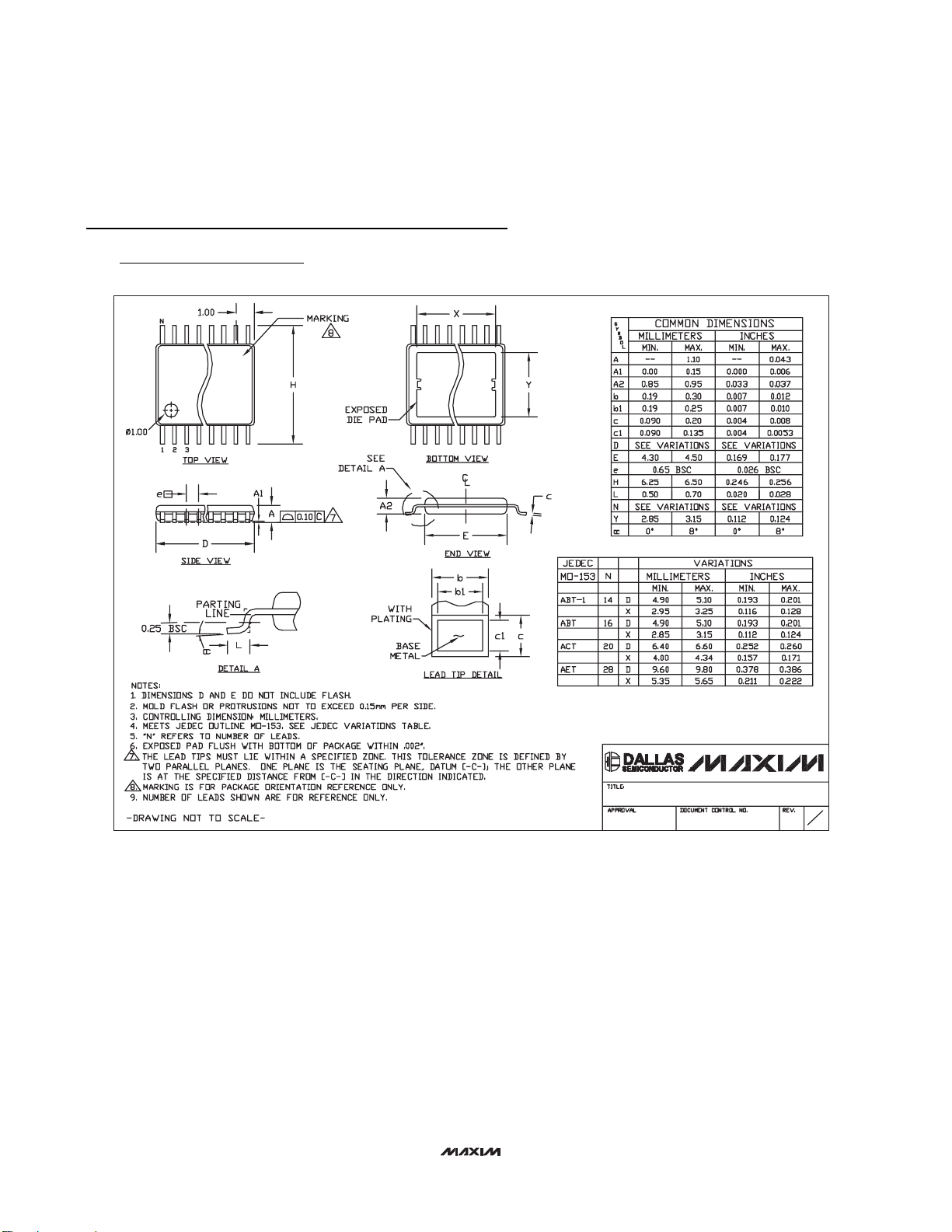
MAX5060/MAX5061
0.6V to 5.5V Output, Parallelable,
Average-Current-Mode DC-DC Controllers
Maxim cannot assume responsibility for use of any circuitry other than circuitry entirely embodied in a Maxim product. No circuit patent licenses are
implied. Maxim reserves the right to change the circuitry and specifications without notice at any time.
Maxim Integrated Products, 120 San Gabriel Drive, Sunnyvale, CA 94086 408-737-7600 ____________________ 31
© 2005 Maxim Integrated Products Printed USA is a registered trademark of Maxim Integrated Products, Inc.
Package Information (continued)
(The package drawing(s) in this data sheet may not reflect the most current specifications. For the latest package outline information
go to www.maxim-ic.com/packages
.)
XX XX
TSSOP 4.4mm BODY.EPS
PACKAGE OUTLINE, TSSOP, 4.40 MM BODY,
EXPOSED PAD
21-0108
1
E
1
 Loading...