

Page 1
现货库存、技术资料、百科信息、热点资讯,精彩尽在鼎好!
General Description
The MAX5058/MAX5059 enable secondary-side synchronous rectification in isolated power supplies using
widely available power MOSFETs. These devices facilitate the commutation of the secondary-side MOSFETs by
providing a clean gate-drive signal that is synchronized
to the power MOSFET switching in the primary side of
the isolation transformer. The MAX5058/MAX5059 complement the MAX5051 and MAX5042/MAX5043 primaryside PWM ICs and enable the design of high-efficiency
synchronously rectified isolated power supplies.
Simultaneous conduction of the primary side and the
freewheeling synchronous rectifier MOSFET is avoided
by having a look-ahead signal (before the primary-side
MOSFETs turn ON), thus eliminating large current spikes
resulting from a shorted transformer secondary.
An on-board error amplifier with a versatile current reference output enables virtually unlimited possibilities in
reference-voltage generation. Reference voltage for the
error amplifier is generated by connecting an appropriate resistor to this output.
Low on-resistance margining MOSFETs integrated onchip allow for implementation of a margining circuit
without the use of external switches. The MAX5058 provides a 5V LDO output for logic-level MOSFETs while
the MAX5059 provides a 10V LDO output for conventional 10V MOSFETs.
The MAX5058/MAX5059 are designed to enable paralleling of multiple power supplies for accurate current
sharing using a simple 2-wire, differential, current-share
bus. Parallelability enables expansion of the power
capabilities and simplifies thermal management in highoutput-current applications. When used in conjunction
with the MAX5051, the primaries can also be synchronized and operated 180 degrees out of phase.
The MAX5058/MAX5059 are available in a 28-pin thermally enhanced TSSOP package and operate over a
wide -40°C to +125°C temperature range.
Warning: The MAX5058/MAX5059 are designed to
work in circuits that contain high voltages. Exercise
caution.
Applications
Isolated Telecom Power Supplies
Isolated Networking Power Supplies
±48V Power-Supply Modules
Industrial Power Supplies
±48V/±12V Server Power Supplies
Features
♦ Clean Drive Waveforms for Synchronous
MOSFETs
♦ Utilization of a Look-Ahead Signal from the
Primary for Proper Turn-On/Turn-Off Times
♦ Synchronous Rectifier Drivers Capable of
Sourcing and Sinking Up to 2A Peak Current
♦ Internal Gate-Voltage Regulator for 5V (MAX5058)
or 10V (MAX5059) Gate-Drive Voltage
♦ Internal Error Amplifier
♦ Accurate Differential Current-Share/Force Circuit
Allows Paralleling of Several Power Supplies for
High Output Current
♦ Internal Remote Voltage-Sense Amplifier
♦ Flexible Reference-Voltage Generation
♦ Output Voltage Regulation Down to 0.5V
♦ Low Quiescent Current Consumption of 2.5mA
♦ Integrated Digital Output Margining Circuit Saves
External Parts and Board Space
♦ 30ns Propagation Delay Time from Pulse Input
to Output
♦ Automatic Detection of Discontinuous Current
Conduction and Turn-Off of the Freewheeling
MOSFET
♦ High Efficiency at Low Output Currents and
Reverse-Current Protection
♦ Open-Drain Overtemperature Warning Flag
♦ 28-Pin Thermally Enhanced TSSOP Package
MAX5058/MAX5059
Parallelable Secondary-Side Synchronous Rectifier
Driver and Feedback-Generator Controller ICs
________________________________________________________________ Maxim Integrated Products 1
19-3045; Rev 0; 10/03
For pricing, delivery, and ordering information, please contact Maxim/Dallas Direct! at
1-888-629-4642, or visit Maxim’s website at www.maxim-ic.com.
Pin Configuration appears at end of data sheet.
Ordering Information
*EP = Exposed paddle.
PART TEMP RANGE
MAX5058AUI -40°C to +125°C 28 TSSOP-EP* 5
MAX5058EUI -40°C to +85°C 28 TSSOP-EP* 5
MAX5059AUI -40°C to +125°C 28 TSSOP-EP* 10
MAX5059EUI -40°C to +85°C 28 TSSOP-EP* 10
PINPACKAGE
V
REG
(V)
Page 2
MAX5058/MAX5059
Parallelable Secondary-Side Synchronous Rectifier
Driver and Feedback-Generator Controller ICs
2 _______________________________________________________________________________________
ABSOLUTE MAXIMUM RATINGS
ELECTRICAL CHARACTERISTICS
(V+ = +12V, GND = PGND = 0, VDR = V
REG
, C
QSYNC
= C
QREC
= 0, ZCP = ZCN = BUFIN = CSP = CSN = SFN = VSN = GND, V
IREF
=
V
VSP
= 1.785V, C
VREG
= 2.2µF, CVP= 1µF, C
COMPS
= 0.1µF, C
SFP
= 68nF, TA= T
MIN
to T
MAX
, unless otherwise noted. Typical values
are at T
A
= +25°C.)
Stresses beyond those listed under “Absolute Maximum Ratings” may cause permanent damage to the device. These are stress ratings only, and functional
operation of the device at these or any other conditions beyond those indicated in the operational sections of the specifications is not implied. Exposure to
absolute maximum rating conditions for extended periods may affect device reliability.
V+ to GND .............................................................-0.3V to +30V
PGND to GND .......................................................-0.3V to +0.3V
COMPV, V
REG
, VDR, TSF to GND......................... -0.3V to +14V
All Other Pins to GND ..................................-0.3V to (VP + 0.3V)
V
REG
Source Current .........................................................50mA
COMPV, RMGU, RMGD, TSF Sink Current ....................... 30mA
VP to GND ................................................................-0.3V to +6V
VSO, CSO Source/Sink Current ......................................... ±5mA
SFP Source Current ............................................................. 5mA
QREC, QSYNC Continuous Current....................................50mA
QREC, QSYNC Current < 500ns..............................................5A
Continuous Power Dissipation (T
A
= +70°C)
28-Pin TSSOP (derate 23.8mW/°C above +70°C). ....1905mW
Junction Temperature......................................................+150°C
Operating Temperature Ranges
MAX5058EUI, MAX5059EUI ............................-40°C to +85°C
MAX5058AUI, MAX5059AUI..........................-40°C to +125°C
Storage Temperature Range .............................-65°C to +150°C
Lead Temperature (soldering, 10s) .................................+300°C
PARAMETER SYMBOL CONDITIONS MIN TYP MAX UNITS
POWER SUPPLY
Supply Voltage Range V+
Quiescent Supply Current I
Switching Supply Current I
I
: REFERENCE CURRENT OUTPUT
REF
Reference Current I
Reference Current Variation ∆I
Reference Voltage Compliance
Range
V
: LOW-DROPOUT REGULATOR
REG
Regulator Output V
Line Regulation
Dropout V
VP: INTERNAL REGULATOR
Regulator Output Setpoint V
ZC: ZERO-CURRENT COMPARATOR
Zero-Current Comparator
Threshold
Zero-Current Comparator Input
Current
MAX5058 4.5 28.0
MAX5059 9.3 28.0
Q
SW
IREF
IREF
VREGIVREG
DROP
V
ZCTH
I
ZC
fSW = 250kHz at BUFIN
V
V
Guaranteed by reference current variation
test
MAX5058, V+ = 6V to 28V 25
MAX5059, V+ = 11V to 28V 25
MAX5058
MAX5059
IVP = 0 to 5mA 3.8 4.3 V
VP
TA = +25°C +3.5 +5 +6.5 mV
= 1.785V 49.2 50 51.1 µA
IREF
= 0.5V to 2.5V -0.1 +0.1 %/V
IREF
= 0 to 30mA
MAX5058 4.5
MAX5059 6
MAX5058 4.75 5 5.25
MAX5059 9.4 10 10.6
V+
I
V+
I
= 4.5V,
VREG
= 9.3V,
VREG
= 30mA
= 30mA
2.5 5 mA
0.5 2.5 V
200 350
200 350
-2.5 +2.5 µA
V
mA
V
mV
mV
Page 3
MAX5058/MAX5059
Parallelable Secondary-Side Synchronous Rectifier
Driver and Feedback-Generator Controller ICs
_______________________________________________________________________________________ 3
ELECTRICAL CHARACTERISTICS (continued)
(V+ = +12V, GND = PGND = 0, VDR = V
REG
, C
QSYNC
= C
QREC
= 0, ZCP = ZCN = BUFIN = CSP = CSN = SFN = VSN = GND, V
IREF
=
V
VSP
= 1.785V, C
VREG
= 2.2µF, CVP= 1µF, C
COMPS
= 0.1µF, C
SFP
= 68nF, TA= T
MIN
to T
MAX
, unless otherwise noted. Typical values
are at T
A
= +25°C.)
PARAMETER SYMBOL CONDITIONS MIN TYP MAX UNITS
Zero-Current Comparator Input
Range
Zero-Current Comparator
Propagation Delay
BUFIN: SYNCHRONIZING PULSE INPUT
BUFIN to Output Propagation
Delay
BUFIN Input Current I
BUFIN Input Capacitance C
BUFIN Input-Logic High V
BUFIN Input-Logic Low V
MARGINING INPUTS
RMGD Resistance R
RMGU Resistance R
MRGD Input-Logic High V
MRGD Input-Logic Low V
MRGU Input-Logic High V
MRGU Input-Logic Low V
MRGU, MRGD Input Resistance
RMGU, RMGD Leakage Current
DRIVER OUTPUTS
QREC, QSYNC Peak Source
Current
QREC, QSYNC Output-Voltage
High
QREC, QSYNC Low-to-High
Delay Time
QREC, QSYNC Peak Sink Current
QREC, QSYNC Output-Voltage
Low
QREC, QSYNC High-to-Low
Delay Time
V
ZC
t
ZC
t
pd
BUFIN
BUFIN
HBUFIN
LBUFIN
RMGD
RMGU
HMRGD
LMRGD
HMRGU
LMRGU
R
MRGD
R
MRGU
I
RMGU
I
RMGD
I
QREC_SO,
I
QSYNC_SO
V
QREC_H,
V
QSYNC_H
t
PDLH
I
QREC_SI,
I
QSYNC_SI
V
QREC_L,
V
QSYNC_L
t
PDHL
10mV overdrive, from when V
greater than V
ZCTH
low
BUFIN rising to QREC rising or QSYNC
falling
Sinking 10mA 6.5 11 Ω
Sinking 10mA 6.5 11 Ω
,
,
Measured with respect to
V
, sourcing 50mA
VDR
C
C
QREC
QREC
= C
= C
= 0 30
QSYNC
= 5nF 70
QSYNC
Sinking 50mA
C
QREC
C
QREC
= C
= C
= 0 40
QSYNC
= 5nF 70
QSYNC
- V
ZCP
ZCN
to when QSYNC goes
MAX5058 75 150
MAX5059 75 150
MAX5058 50 100
MAX5059 50 100
-0.1 +1.5 V
is
65 ns
40 ns
-1 +1 µA
10 pF
2.4 V
0.8 V
2.4 V
0.8 V
2.4 V
0.8 V
40 kΩ
-100 +100 nA
2A
2A
mV
ns
mV
ns
Page 4
MAX5058/MAX5059
Parallelable Secondary-Side Synchronous Rectifier
Driver and Feedback-Generator Controller ICs
4 _______________________________________________________________________________________
ELECTRICAL CHARACTERISTICS (continued)
(V+ = +12V, GND = PGND = 0, VDR = V
REG
, C
QSYNC
= C
QREC
= 0, ZCP = ZCN = BUFIN = CSP = CSN = SFN = VSN = GND, V
IREF
=
V
VSP
= 1.785V, C
VREG
= 2.2µF, CVP= 1µF, C
COMPS
= 0.1µF, C
SFP
= 68nF, TA= T
MIN
to T
MAX
, unless otherwise noted. Typical values
are at T
A
= +25°C.)
)
PARAMETER SYMBOL CONDITIONS MIN TYP MAX UNITS
ERROR AMPLIFIER
Inverting Input Current I
Error-Amplifier Input Range V
Error-Amplifier Input Offset V
Error-Amplifier Output-Voltage
Low
Error-Amplifier Unity-Gain BW GBW R
Error-Amplifier Voltage Gain A
Error-Amplifier PSRR PSRR 60 dB
COMPV Output Resistance to
Ground
REMOTE-SENSE AMPLIFIER (RSA)
VSN Input Current I
VSP Input Current I
Input Common-Mode Range -0.3 +3.8 V
Input Offset Voltage V
Output Impedance 8 Ω
Amplifier -3dB Frequency I
Remote-Sense Amplifier Gain G
CURRENT-SENSE AMPLIFIER (CSA)
CSN Input Current I
CSP Input Current I
Input Offset Voltage I
Current-Sense Amplifier Gain G
Input Differential-Mode Range 100 mV
Input Common-Mode Range -0.3 +3.8 V
Output-Voltage Level Shift V
Output Voltage Range V
Amplifier -3dB Frequency f
SHARE-FORCE AMPLIFIER (SFA)
Sink Current 60 µA
Source Current 500 µA
INV
INV
I
OS
V
COMPVICOMPV
VOL
COMPV
COMP
R
COMPV
(Note 1) 1 MΩ
VSN
VSP
OSRSAIVSO
VSO
I
RS
CSN
CSP
CSAICSO
LS
CSO(MIN
-3dB
VSO
-0.3V ≤ V
-0.3V ≤ V
-0.3V ≤ V
CSO
(Note 2) 0.415 0.570 V
I
CSO
I
CSO
-50 +50 nA
0 2.5 V
= 100µA to 5mA -5 +5 mV
= 5mA 200 mV
= 220Ω, I
= 220Ω, I
= 5mA 1.3 MHz
COMP
= 5mA 80 dB
COMP
-100 +100 µA
-20 +100 µA
= -0.5mA to +0.5mA -4 mV
= -0.5mA to +0.5mA 1 MHz
= -0.5mA to +0.5mA 0.9925 1 1.0075 V/V
≤ +3.8V,
CSN
≤ +3.8V
CSP
≤ +3.8V -40 +150 µA
CSP
-150 +150 µA
= -500µA to +500µA (Note 2) +20 +25 +30 mV
= -500µA to +500µA 19.8 20 20.2 V/V
= -500µA to +500µA 0.1 3.0 V
= -500µA to +500µA 50 kHz
Page 5
MAX5058/MAX5059
Parallelable Secondary-Side Synchronous Rectifier
Driver and Feedback-Generator Controller ICs
_______________________________________________________________________________________ 5
Note 1: Output resistance to ground used for unity-gain stability.
Note 2: V
CSO
= G
CSA(VCSP
- V
CSN
) + VLS.
ELECTRICAL CHARACTERISTICS (continued)
(V+ = +12V, GND = PGND = 0, VDR = V
REG
, C
QSYNC
= C
QREC
= 0, ZCP = ZCN = BUFIN = CSP = CSN = SFN = VSN = GND, V
IREF
=
V
VSP
= 1.785V, C
VREG
= 2.2µF, CVP= 1µF, C
COMPS
= 0.1µF, C
SFP
= 68nF, TA= T
MIN
to T
MAX
, unless otherwise noted. Typical values
are at T
A
= +25°C.)
PARAMETER SYMBOL CONDITIONS MIN TYP MAX UNITS
CURRENT-ADJUST AMPLIFIER (CAA)
Transconductance 500 µA/V
Common-Mode Input Voltage
Range
Output Voltage Range 0.85 2.75 V
Offset Voltage TA = +25°C204265mV
Open-Loop Gain 72 dB
CURRENT-ADJUST VOLTAGE-TO-CURRENT CONVERTER
Input Voltage Range 0.75 2.75 V
Input Voltage Offset 1.25 V
Output Voltage Range 0.5 2.5 V
Transconductance 1.15 µA/V
Maximum Current Adjustment
Value
THERMAL SHUTDOWN
Thermal Warning Flag Level When TSF pulls low +125 °C
Thermal Warning Flag Hysteresis 15 °C
Internal Thermal-Shutdown Level +160 °C
Internal Thermal-Shutdown
Hysteresis
TSF Maximum Output Voltage I
TSF Output Leakage Current 0.1 µA
= 5mA 120 mV
TSF
0.45 2.55 V
1.38 1.5 1.66 µA
15 °C
Page 6
MAX5058/MAX5059
Parallelable Secondary-Side Synchronous Rectifier
Driver and Feedback-Generator Controller ICs
6 _______________________________________________________________________________________
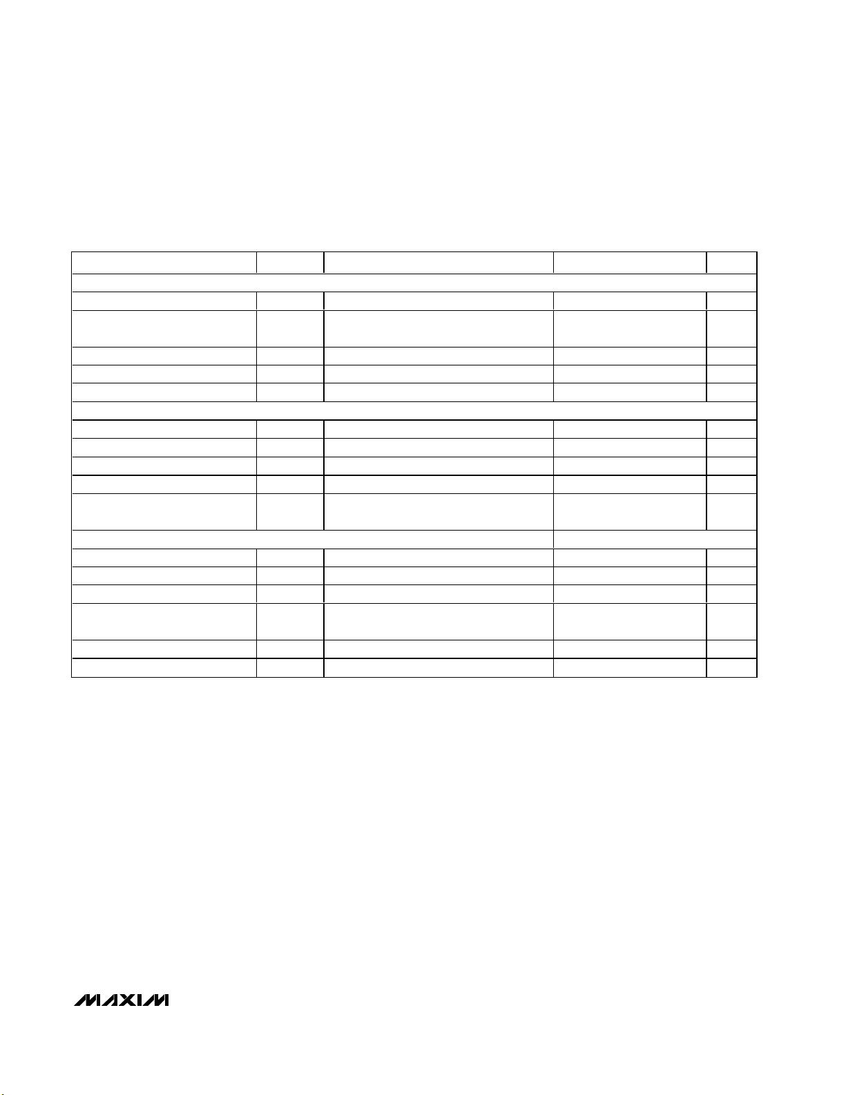
Typical Operating Characteristics
(V+ = +12V, GND = PGND = 0, VDR = V
REG
, C
QSYNC
= C
QREC
= 0, ZCP = ZCN = BUFIN = CSP = CSN = SFN = VSN = GND, V
IREF
=
V
VSP
= 1.785V, V
COMPS
= 0.5V, C
VREG
= 2.2µF, CVP= 1µF, C
COMPS
= 0.1µF, C
SFP
= 68nF, TA= +25°C, unless otherwise noted.)
LDO OUTPUT VOLTAGE (V
VREG
)
vs. INPUT VOLTAGE (MAX5058)
MAX5058/59 toc01
V+ (V)
V
VREG
(V)
272418 216 9 12 153
4.9995
5.0000
5.0005
5.0010
5.0015
5.0020
5.0025
5.0030
5.0035
5.0040
5.0045
5.0050
4.9990
030
I
VREG
= 0mA
I
REF
OUTPUT CURRENT
vs. TEMPERATURE
MAX5058/59 toc02
TEMPERATURE (°C)
I
REF
(µA)
1109565 80-10 5 20 35 50-25
49.95
49.97
49.99
50.01
50.03
50.05
50.07
50.09
50.11
50.13
50.15
50.17
49.93
-40 125
V
IREF
= 1.785V
LDO OUTPUT VOLTAGE (V
VREG
)
vs. LOAD CURRENT (MAX5059)
MAX5058/59 toc03
I
VREG
(mA)
V
VREG
(V)
1009070 8020 30 40 50 6010
9.84
9.86
9.88
9.90
9.92
9.94
9.96
9.98
10.00
10.02
10.04
10.06
10.08
10.10
9.82
9.80
0 110
LDO OUTPUT VOLTAGE (V
VREG
)
vs. LOAD CURRENT (MAX5058)
MAX5058/59 toc04
I
VREG
(mA)
V
VREG
(V)
1009070 8020 30 40 50 6010
4.88
4.90
4.92
4.94
4.96
4.98
5.00
5.02
5.04
4.86
0 110
LDO OUTPUT VOLTAGE (V
REG
)
vs. TEMPERATURE (MAX5058)
MAX5058/59 toc05
TEMPERATURE (°C)
V
VREG
(V)
1109565 80-10 15 20 35 50-25
4.984
4.986
4.988
4.990
4.992
4.994
4.996
4.998
5.000
5.002
5.004
5.006
5.008
5.010
4.982
4.980
-40 125
LDO OUTPUT VOLTAGE (V
VREG
)
vs. INPUT VOLTAGE (MAX5059)
MAX5058/59 toc06
V+ (V)
V
VREG
(V)
272418 216 9 12 153
10.000
10.002
10.004
10.006
10.008
10.010
10.012
10.014
10.016
10.018
10.020
9.998
030
LDO OUTPUT VOLTAGE (V
VREG
)
vs. TEMPERATURE (MAX5059)
MAX5058/59 toc07
TEMPERATURE (°C)
V
VREG
(V)
1109565 80-10 5 20 35 50-25
9.985
9.990
9.995
10.000
10.005
10.010
10.015
10.020
10.025
10.030
9.980
-40 125
I
REF
OUTPUT CURRENT
vs. I
REF
OUTPUT VOLTAGE
MAX5058/59 toc08
V
IREF
(V)
I
IREF
(µA)
3.53.02.0 2.51.0 1.50.5
46.5
47.0
47.5
48.0
48.5
49.0
49.5
50.0
50.5
51.0
46.0
0 4.0
Page 7
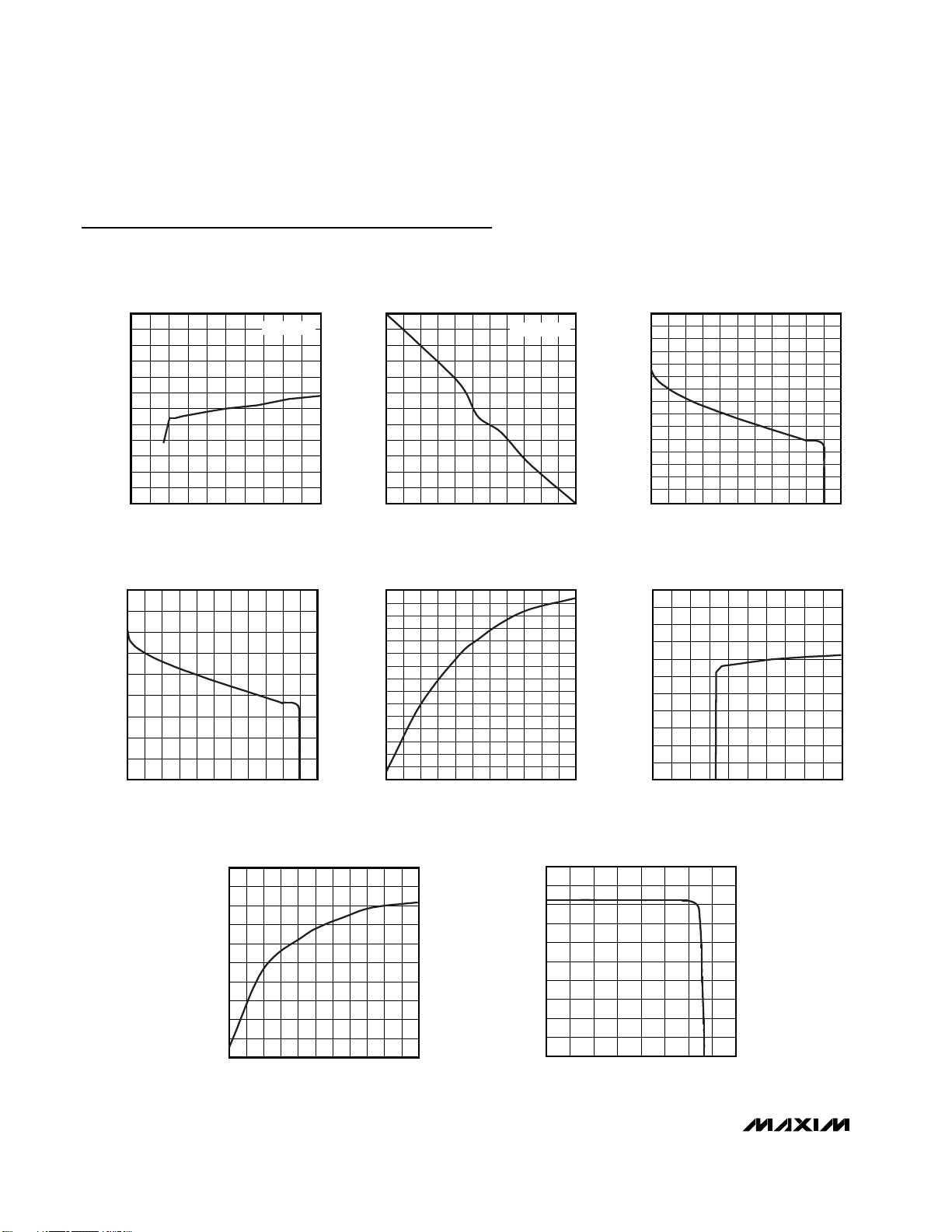
SWITCHING SUPPLY CURRENT
vs. TEMPERATURE (MAX5058)
MAX5058/59 toc14
TEMPERATURE (°C)
I
V+
(mA)
1109565 80-10 5 20 35 50-25
3.2
3.4
3.6
3.8
4.0
4.2
4.4
4.6
4.8
5.0
3.0
-40 125
fSW = 250kHz
SWITCHING SUPPLY CURRENT
vs. INPUT VOLTAGE (MAX5059)
MAX5058/59 toc15
V+ (V)
I
V+
(mA)
2723 259 11131517192157
0.5
1.0
1.5
2.0
2.5
3.0
3.5
4.0
4.5
5.0
5.5
6.0
0
329
fSW = 250kHz
QUIESCENT SUPPLY CURRENT
vs. TEMPERATURE (MAX5059)
MAX5058/59 toc12
TEMPERATURE (°C)
I
V+
(mA)
1109565 80-10 5 20 35 50-25
2.1
2.2
2.3
2.4
2.5
2.6
2.7
2.8
2.9
3.0
2.0
-40 125
SWITCHING SUPPLY CURRENT
vs. INPUT VOLTAGE (MAX5058)
MAX5058/59 toc13
V+ (V)
I
V+
(mA)
2723 2591113151719215
7
0.5
1.0
1.5
2.0
2.5
3.0
3.5
4.0
4.5
5.0
0
329
fSW = 250kHz
MAX5058/MAX5059
Parallelable Secondary-Side Synchronous Rectifier
Driver and Feedback-Generator Controller ICs
_______________________________________________________________________________________ 7
Typical Operating Characteristics (continued)
(V+ = +12V, GND = PGND = 0, VDR = V
REG
, C
QSYNC
= C
QREC
= 0, ZCP = ZCN = BUFIN = CSP = CSN = SFN = VSN = GND, V
IREF
=
V
VSP
= 1.785V, V
COMPS
= 0.5V, C
VREG
= 2.2µF, CVP= 1µF, C
COMPS
= 0.1µF, C
SFP
= 68nF, TA= +25°C, unless otherwise noted.)
QUIESCENT SUPPLY CURRENT
vs. INPUT VOLTAGE (MAX5058)
3.0
2.8
2.6
2.4
2.2
2.0
1.8
1.6
(mA)
1.4
V+
I
1.2
1.0
0.8
0.6
0.4
0.2
0
030
V+ (V)
3.0
2.8
2.6
2.4
MAX5058/59 toc09
2.2
2.0
1.8
1.6
(mA)
V+
1.4
I
1.2
1.0
0.8
0.6
0.4
0.2
0
272418 216 9 12 153
030
QUIESCENT SUPPLY CURRENT
vs. INPUT VOLTAGE (MAX5059)
QUIESCENT SUPPLY CURRENT
vs. TEMPERATURE (MAX5058)
2.60
2.55
2.50
MAX5058/59 toc10
2.45
2.40
2.35
(mA)
2.30
V+
I
2.25
2.20
2.15
2.10
2.05
272418 216 9 12 153
V+ (V)
2.00
-40 125
TEMPERATURE (°C)
1109565 80-10 5 20 35 50-25
MAX5058/59 toc11
Page 8
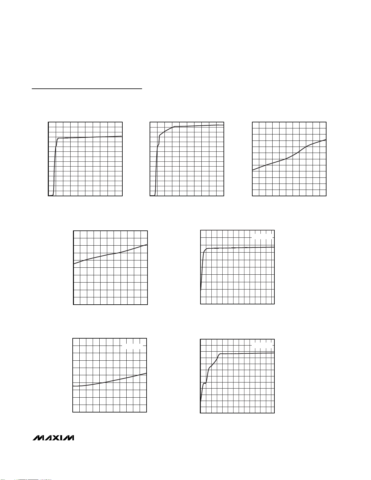
MAX5058/MAX5059
Parallelable Secondary-Side Synchronous Rectifier
Driver and Feedback-Generator Controller ICs
8 _______________________________________________________________________________________
Typical Operating Characteristics (continued)
(V+ = +12V, GND = PGND = 0, VDR = V
REG
, C
QSYNC
= C
QREC
= 0, ZCP = ZCN = BUFIN = CSP = CSN = SFN = VSN = GND, V
IREF
=
V
VSP
= 1.785V, V
COMPS
= 0.5V, C
VREG
= 2.2µF, CVP= 1µF, C
COMPS
= 0.1µF, C
SFP
= 68nF, TA= +25°C, unless otherwise noted.)
SWITCHING SUPPLY CURRENT
vs. TEMPERATURE (MAX5059)
MAX5058/59 toc16
TEMPERATURE (°C)
I
V+
(mA)
1109565 80-10 5 20 35 50-25
4.2
4.4
4.6
4.8
5.0
5.2
5.4
5.6
5.8
6.0
4.0
-40 125
fSW = 250kHz
REMOTE-SENSE AMPLIFIER (RSA) GAIN
vs. TEMPERATURE
MAX5058/59 toc17
TEMPERATURE (°C)
VSO OUTPUT (dB)
11095-25 -10 5 35 50 6520 80
0.008
0.009
0.010
0.011
0.012
0.013
0.014
0.015
0.007
-40 125
V
VSP
= 1.785V
RSA GAIN
vs. FREQUENCY
MAX5058/59 toc18
FREQUENCY (Hz)
GAIN (dB)
10M1M10k 100k1k0.1k
-35
-30
-25
-20
-15
-10
-5
0
5
10
-40
0 100M
CSA GAIN
vs. FREQUENCY
MAX5058/59 toc21
FREQUENCY (Hz)
GAIN (dB)
1k1001010.1
-15
-10
-5
0
5
10
15
20
25
30
-20
0.01 10k
ZERO-CURRENT COMPARATOR THRESHOLD
vs. TEMPERATURE
MAX5058/59 toc22
TEMPERATURE (°C)
ZCP THRESHOLD (mV)
11095-25 -10 5 35 50 6520 80
5.05
5.10
5.15
5.20
5.25
5.30
5.35
5.40
5.00
-40 125
CURRENT-SENSE AMPLIFIER (CSA) GAIN
vs. TEMPERATURE
MAX5058/59 toc19
TEMPERATURE (°C)
CSA GAIN (V/V)
11095-25 -10 5 35 50 6520 80
19.97
19.98
19.99
20.00
20.01
20.02
20.03
20.04
19.96
-40 125
V
CSP
= 100mV
CSA INPUT OFFSET
vs. TEMPERATURE
MAX5058/59 toc20
TEMPERATURE (°C)
INPUT OFFSET (mV)
1109565 80-10 5 20 35 50-25
24.1
24.2
24.3
24.4
24.5
24.6
24.7
24.8
24.9
25.0
25.1
24.0
-40 125
Page 9

MAX5058/MAX5059
Parallelable Secondary-Side Synchronous Rectifier
Driver and Feedback-Generator Controller ICs
_______________________________________________________________________________________ 9
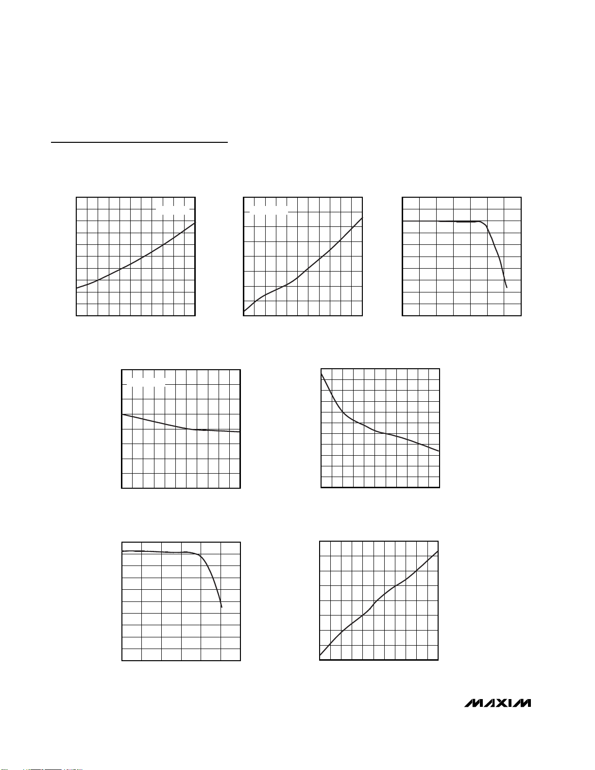
Typical Operating Characteristics (continued)
(V+ = +12V, GND = PGND = 0, VDR = V
REG
, C
QSYNC
= C
QREC
= 0, ZCP = ZCN = BUFIN = CSP = CSN = SFN = VSN = GND, V
IREF
=
V
VSP
= 1.785V, V
COMPS
= 0.5V, C
VREG
= 2.2µF, CVP= 1µF, C
COMPS
= 0.1µF, C
SFP
= 68nF, TA= +25°C, unless otherwise noted.)
BUFIN TO QREC LOW-TO-HIGH
PROPAGATION DELAY vs. TEMPERATURE
MAX5058/59 toc26
TEMPERATURE (°C)
PROPAGATION DELAY (ns)
1109565 80-10 5 20 35 50-25
29
30
31
32
33
34
35
36
37
38
39
40
41
42
28
-40 125
BUFIN TO QREC HIGH-TO-LOW
PROPAGATION DELAY vs. TEMPERATURE
MAX5058/59 toc27
TEMPERATURE (°C)
PROPAGATION DELAY (ns)
1109565 80-10 5 20 35 50-25
34
36
38
40
42
44
46
48
50
52
54
56
58
60
32
30
-40 125
BUFIN TO QSYNC LOW-TO-HIGH
PROPAGATION DELAY vs. TEMPERATURE
MAX5058/59 toc28
TEMPERATURE (°C)
PROPAGATION DELAY (ns)
1109565 80-10 5 20 35 50-25
48
50
52
54
56
58
60
44
42
40
46
-40 125
BUFIN TO QSYNC HIGH-TO-LOW
PROPAGATION DELAY vs. TEMPERATURE
MAX5058/59 toc29
TEMPERATURE (°C)
PROPAGATION DELAY (ns)
1109565 80-10 5 20 35 50-25-40 125
28
30
32
34
36
38
40
24
22
20
26
ZERO-CURRENT PROPAGATION DELAY
vs. TEMPERATURE
90
10mV OVERDRIVE
85
80
75
70
65
ZCP TO QSYNC DELAY (ns)
60
55
50
-40 125
TEMPERATURE (°C)
11095-25 -10 5 35 50 6520 80
MAX5058/59 toc23
SFA AMPLIFIER MAXIMUM
SINK CURRENT vs. TEMPERATURE
34.0
33.8
33.6
33.4
33.2
33.0
32.8
32.6
SFA SINK CURRENT (µA)
32.4
32.2
32.0
-40 125
CURRENT-ADJUST VOLTAGE TO CURRENT-
CONVERTER ADJUSTMENT RANGE
vs. TEMPERATURE
1.60
TEMPERATURE (°C)
SFP = +2.5V
SFN = 0V
1109565 80-10 5 20 35 50-25
MAX5058/59 toc24
1.59
1.58
1.57
1.56
1.55
1.54
1.53
ADJUSTMENT RANGE (µA)
1.52
1.51
1.50
-40 125
TEMPERATURE (°C)
1109565 80-10 5 20 35 50-25
MAX5058/59 toc25
Page 10

MAX5058/MAX5059
Parallelable Secondary-Side Synchronous Rectifier
Driver and Feedback-Generator Controller ICs
10 ______________________________________________________________________________________
Pin Description
PIN
FUNCTION
1 ZCP
Zero-Inductor Current-Sense Comparator Input. The source voltage of the freewheeling FET (N4 in the Typical
Application Circuit) is sensed. The gate drive is terminated when this voltage becomes positive during a primary
power-OFF cycle.
2
Zero-Inductor Current-Sense Comparator Negative Input
3
Ground Connection
4 SFN
Negative Input of the Share-Force Amplifier. Connect the SFN inputs together from all the power-supply
secondaries, then connect to the load return terminal (isolated GND). Connect to GND when current sharing is not
used.
5 SFP
Positive Input of the Share-Force Amplifier. Connect the SFP pins together from all the power-supply secondaries.
Leave this pin unconnected when current sharing is not used.
6
Compensation Output of the Load-Share Transconductance Amplifier
7 TSF Thermal Warning Flag Output
8
Margin-Up Logic Input. When toggled high, the power-supply output voltage is set to the high margin.
9
Margin-Down Logic Input. When toggled high, the power-supply output voltage is set to the low margin.
10
Resistor Connection for Margin-Down
11
Resistor Connection for Margin-Up
12
I
REF
Reference Current Output. A resistor from this current source output to GND sets the reference voltage used by
the error amplifier.
13
Compensation Connection for the Error Amplifier. The feedback optocoupler LED is also connected to this point.
This open-drain output is capable of sinking at least 5mA.
14
INV
Inverting Input of the Error Amplifier. A voltage-divider connected to this input scales the power-supply output
voltage for regulation.
15
Output of the Remote-Sense Amplifier
16
VSN Negative Input of the Remote-Sense Amplifier. Connect this to the negative terminal of the load.
17
VSP Positive Input of the Remote-Sense Amplifier. Connect this to the positive terminal of the load.
18
Output of the Current-Sense Amplifier. It can be used to monitor the output current.
19
Connect this input to the negative terminal of the output current-sense resistor. Connect to GND when not used.
20
CSP Connect this input to the positive terminal of the output current-sense resistor. Connect to GND when not used.
21
VP
Compensation Pin for Internal +4V Preregulator. A minimum 1µF low-ESR capacitor must be connected to this pin
for bypassing.
22
V+
Supply Connection for the IC and Input to the Internal 5V (MAX5058) or 10V (MAX5059) Regulator. Maximum
voltage on this input is 28V.
23
Regulated +5V (MAX5058) or +10V(MAX5059) Output Used by the Internal Circuitry and the Output Drivers. A
minimum 1µF capacitor must be connected to this pin for bypassing.
24
Input for the Synchronizing Pulse. This pulse is provided by the primary-side power IC.
25
Supply Connection for the Output Drivers. Can be connected to V
REG
for 5V (MAX5058) or 10V (MAX5059)
operation.
26
Driver Output for the Rectifying MOSFET
27
Power-Ground Connection. Return ground connection for the gate-driver pulse currents.
28
Driver Output for the Recirculating MOSFET
—
EP
Exposed Pad. This is the exposed pad on the underside of the IC. Connect the exposed paddle to GND and to a
large copper ground plane to aid in heat dissipation.
NAME
ZCN
GND
COMPS
MRGU
MRGD
RMGD
RMGU
COMPV
VSO
CSO
CSN
V
REG
BUFIN
VDR
QREC
PGND
QSYNC
Page 11

MAX5058/MAX5059
Parallelable Secondary-Side Synchronous Rectifier
Driver and Feedback-Generator Controller ICs
______________________________________________________________________________________ 11
Figure 1. MAX5058/MAX5059 Functional Diagram
MARGINING BLOCK
8MRGU
9MRGD
10RMGD
RMGU
11
13
COMPV
14INV
12I
REF
6COMPS
50kΩ
50kΩ
QMD
QMU
ERROR AMPLIFIER BLOCK
E/A
I
REF
50µA
REFERENCE CURRENT BLOCK
MAX5058/MAX5059
REGULATOR AND THERMAL MANAGEMENT BLOCK
SD DRIVERS
CURRENT-SHARE BLOCK
V TO I
SHUTDOWN
500µS
I = (1.15 x (V
V
CAA
UVLO AND
THERMAL
CAA
≥ 1.25V
- 1.25))µA
CAA
42mV
LDO
5V/10V
R
0.5V
22 V+
PREG
4V
+125°C FLAG
R
SFA
RR
X1
X2
21
23
7 TSF
5
4
20
10
18
VP
V
SFP
SFN
CSP
CSN
CSO
REG
REMOTE-SENSE AMPLIFIER BLOCK
15
VSO
16
VSN
X1
17VSP
GATE-DRIVER BLOCK
BUFIN
124ZCP
2
ZCN
GND
3
RSA
20ns
5mV
20ns
SD DRIVERS
30ns FALLING
EDGE DELAY
25
VDR
QREC
26
QSYNC
28
PGND
27
Page 12

MAX5058/MAX5059
Parallelable Secondary-Side Synchronous Rectifier
Driver and Feedback-Generator Controller ICs
12 ______________________________________________________________________________________
Detailed Description
The MAX5058/MAX5059 enable the design of high-efficiency, isolated power supplies using synchronous rectification on the secondary side. These devices
commutate the secondary-side MOSFETs by providing
a clean gate-drive signal that is synchronized to the
power MOSFET switching in the primary side of the isolation transformer. Once fully enhanced, the secondaryside MOSFETs have very low on-resistance, producing
a voltage drop much lower than Schottky diodes, resulting in much higher efficiencies. Simultaneous conduction of the synchronous rectifier MOSFETs is avoided by
having a look-ahead signal before the primary
MOSFETs turn on. This eliminates large current spikes
from a shorted transformer secondary.
The MAX5058 has a 5V internal gate-drive voltage regulator that can be used with logic-level MOSFETs. The
MAX5059 has a 10V internal gate-drive voltage regulator that can be used with high-gate-voltage MOSFETs.
In addition to the gate drivers, there are blocks that
make the MAX5058/MAX5059 complete secondaryside solutions. These blocks are as follows:
• Regulator and thermal-management block
• Buffer input and gate-driver block
• Reference-current block
• Error-amplifier block
• Margining block
• Remote-sense amplifier block
• Current-share block
Regulators and Thermal Management
The linear regulators in the MAX5058/MAX5059 provide
power for the internal circuitry, as well as power for running the external synchronous MOSFETs. Design is simplified by deriving the power from the secondary
winding before the output-filter inductor. The peak voltage at the secondary is at least twice the output voltage, yielding more than 7V peak even for output
voltages down to 3.3V. Use a diode and a capacitor to
rectify and filter the voltage before applying it to V+ (see
D6 and C32 in the Typical Application Circuit). The
input for the regulator is V+ and the output is V
REG
.
Connect VDR to V
REG
to provide the supply for the gate
driver’s QREC and QSYNC. For logic-level MOSFETs,
use the MAX5058. For conventional MOSFETs that
require 10V to be fully enhanced, use the MAX5059.
The V+ input voltage range is from +4.5V to +28V.
Supply enough current to this input to satisfy the quies-
cent supply current of the MAX5058/MAX5059, as well
as the current for the MOSFET drivers. Estimate the total
required supply current by using the following formula:
where I
V+
is the current that must be supplied into V+
and QN3, QN4are the total gate charges of MOSFETs
N3 and N4 in the Typical Application Circuit. fSWis the
switching frequency and I
SW
is the switching current of
the part. Use high-quality ceramic capacitors to bypass
V+ and V
REG
. Use additional capacitance as required
for bypassing switching currents generated by the drivers when driving the chosen MOSFETs. Connect at
least a 1µF ceramic capacitor at the output of the regulator V
REG
for stability.
The MAX5058/MAX5059 have an exposed pad at the
back of the package to enable heatsinking directly to a
ground plane. When soldered to a 1in2copper island,
these devices are able to dissipate approximately 1.9W
at +70°C ambient temperature. Connect the exposed
pad to the GND.
In addition to the regulators, this block contains a thermal-shutdown circuit that shuts down the gate drivers if
the die temperature exceeds +160°C. This is a last
resort shutdown mechanism. The trigger of this shutdown mechanism must be avoided. Turning off the
secondary synchronous rectifier drivers in this manner
while the output carries the full load current causes the
current to be diverted to the lossy external diodes or
body diodes of the MOSFETs. This, in most cases,
leads to rectifier failure due to power dissipation. To
prevent this, make use of the TSF output (temperature
warning flag). TSF is an open-drain output that gets
asserted when the die temperature exceeds +125°C,
well before the actual thermal shutdown at +160°C. An
optocoupler connected from V
REG
to the TSF pin can
provide a means for shutting down the switching at the
primary side, thus avoiding catastrophic failure.
Buffer Input (BUFIN) and MOSFET Drivers
The MAX5058/MAX5059 drive external N-channel
MOSFETs at QSYNC and QREC. The QSYNC output
drives the gate of the freewheeling MOSFET N4 in the
Typical Application Circuit. The QREC output drives the
gate of the rectifying MOSFET N3 in the Typical
Application Circuit. Each gate-driver output is capable
of sinking and sourcing up to 2A peak current,
enabling the MAX5058/MAX5059 to drive high-gatecharge MOSFETs.
II f QQ
VSWSW N N+
=+× +
()
34
Page 13

The MOSFET drivers are synchronized to the primaryside switching by using the BUFIN input. BUFIN
accepts the PWM information from the primary through
a high-speed optocoupler or through a small isolation
pulse transformer. Figures 2 through 6 show the interface details using an optocoupler or a pulse transformer with two different kinds of primary-side PWM
controllers.
For proper operation, the MAX5051, MAX5042, and
MAX5043 devices generate a look-ahead signal that
precedes the actual switching of the primary MOSFETs
by a small amount of time, typically less than 100ns.
Additional circuitry may be required when the
MAX5058/MAX5059 are used with other primary-side
controllers not capable of providing a look-ahead signal.
When BUFIN goes high, QREC goes high and QSYNC
goes low. When BUFIN goes low, QREC goes low and
QSYNC goes high.
The MAX5058/MAX5059 provide improved efficiency at
light loads by allowing discontinuous conduction operation. A zero-crossing comparator with inputs ZCP and
ZCN monitors the current through the freewheeling
MOSFET using a sense resistor at its source. The freewheeling MOSFET is turned off when the inductor current is near zero. The actual threshold can be externally
adjusted. The Typical Application Circuit shows one
method for trip-point adjustment using components
R31 and R34.
BUFIN is internally clamped to 4V. Use a voltage-divider,
if necessary, to reduce any external voltage applied to
this pin to less than 4V.
MAX5058/MAX5059
Parallelable Secondary-Side Synchronous Rectifier
Driver and Feedback-Generator Controller ICs
______________________________________________________________________________________ 13
Figure 3. Interface of MAX5059 to MAX5042/MAX5043 Using a High-Speed Optocoupler
Figure 2. Interface of MAX5058 to MAX5042/MAX5043 Using a High-Speed Optocoupler
MAX5042
MAX5043
REG5
PPWM
PWMNEG
BSS84
560Ω
2kΩ
PS9715
OR EQUIVALENT
HIGH-SPEED
OPTOCOUPLER
MAX5058
V
(5V)
REG
330Ω
BUFIN
GND
MAX5042
MAX5043
REG5
PPWM
PWMNEG
BSS84
560Ω
2kΩ
PS9715
OR EQUIVALENT
HIGH-SPEED
OPTOCOUPLER
MMBT3904
1µF
3.10kΩ
4.42kΩ
330Ω
V
REG
BUFIN
GND
MAX5059
(10V)
Page 14

MAX5058/MAX5059
Parallelable Secondary-Side Synchronous Rectifier
Driver and Feedback-Generator Controller ICs
14 ______________________________________________________________________________________
Figure 4. Interface of MAX5058 to MAX5051 Using a High-Speed Optocoupler
Figure 5. Interface of MAX5059 to MAX5051 Using a High-Speed Optocoupler
Figure 6. Interface Circuit to MAX5051 Using a Pulse Transformer
LXH
GND
4.7Ω
2kΩ
BSS84
560Ω
1µF
2kΩ
OR EQUIVALENT
HIGH-SPEED
OPTOCOUPLER
MAX5051 MAX5058
REG5
LXVDD
LXH
GND
4.7Ω
2kΩ
BSS84
560Ω
1µF
2kΩ
PS9715
OR EQUIVALENT
HIGH-SPEED
OPTOCOUPLER
MAX5051
REG5
LXVDD
PS9715
MMBT3904
1µF
330Ω
3.10kΩ
330Ω
4.42kΩ
V
REG
BUFIN
GND
(5V)
V
REG
BUFIN
GND
MAX5059
(10V)
MAX5051 MAX5058
REG5
LXVDD
LXH
GND
LXL
4.7Ω
D1
D2
1µF
T1
T1: PULSE ENGINEERING, PE-68386
D1, D2: CENTRAL SIMICONDUCTOR, CMOSH-3
MAX5059
301Ω1N4148
BUFIN
2kΩ
GND
Page 15

Reverse-Current Prevention
in Synchronous Rectifiers
One benefit of secondary-side synchronous rectification is increased efficiency. Another benefit is that it
allows the inductor current to remain continuous
throughout the operating load range. This results in
constant loop dynamics that are easy to compensate.
In some cases, it may be necessary to turn off the freewheeling MOSFET when the current through this device
attempts to flow from drain to source. Turning off this
MOSFET can be done to enhance efficiency at low output current. When multiple power supplies are paralleled, the power supply with the highest output voltage
has a tendency to source current into the power-supply
outputs with lower output voltage. Turning off the freewheeling MOSFET also prevents this current back-flow.
When the inductor current is allowed to become discontinuous, the loop dynamics change and the circuit
must be compensated accordingly to accommodate
stable continuous and discontinuous mode operation.
Turning off the freewheeling MOSFET is accomplished
by using the zero-current comparator (pins ZCP and
ZCN). Use this comparator to sense reverse current in
the freewheeling MOSFET and turn off the device by
pulling QSYNC low. An internal latch prevents the freewheeling MOSFET from turning on until the off-time of
the next cycle.
Reference Current
The MAX5058/MAX5059 do not have an explicit reference voltage generator. Instead, they contain a 1%accurate trimmed 50µA current source. This allows significant flexibility in setting the reference voltage. In
some cases, the output-voltage resistive divider, consisting of R1 and R2 in the Typical Application Circuit,
can be eliminated by selecting a suitable resistor value
at the I
REF
pin. This reduces the error that the output
voltage-divider may add. Use a low-value bypass
capacitance at this pin to eliminate noise. Typical values
for this capacitance are calculated by considering the
pole that it presents with R12. This pole must be placed
well beyond the frequency range of interest of the current-share loop. Use values less than 2.2nF.
Error Amplifier
The MAX5058/MAX5059 incorporate a 1.3MHz unity
gain-bandwidth error amplifier with inputs INV, I
REF
,
and output COMPV. I
REF
is the noninverting input and
also serves as the reference voltage generator with the
internal 50µA current source and the external resistor
connected from I
REF
to GND. INV is the inverting input
and connects to the center of a resistive divider from
OUT to INV to GND. The output of the error amplifier,
COMPV, connects to the cathode of the LED in the
optocoupler to control the diode current that transmits
the error signal back to the primary-side controller. An
open-drain-output error amplifier simplifies interfacing
with the feedback optocoupler. Use this error amplifier
the same way as the industry-standard TL431 shunt reference. The open-drain output provides flexibility that
may be necessary when additional functionality such
as secondary current-limit regulation is required. Unlike
the TL431, the output of the internal error amplifier of
the MAX5058/MAX5059 is guaranteed to be a maximum of 200mV with a 5mA drain current, compared to
2.5V for the TL431 and 1.24V for the TLV431.
In some cases, it is possible to avoid the use of the output voltage-divider (R1 and R2) by connecting INV to
the output through just R1. This eliminates the voltage
tolerance errors caused by R1 and R2. Output voltage
in this configuration is set directly by using a suitable
resistor at I
REF
. Figure 7 shows this configuration.
MAX5058/MAX5059
Parallelable Secondary-Side Synchronous Rectifier
Driver and Feedback-Generator Controller ICs
______________________________________________________________________________________ 15
Figure 7. Output Voltage Regulation for 0.5V ≤ V
OUT
≤ 2.5V
I
REF
50µA
I
INV
REF
C28
13
14
V
= (50µA) x R12
OUT
FOR: 0.5V ≤ V
12
R12
COMPV
E/A
OUT
≤ 2.5V
V
OUT
R1
Page 16

Figure 8 shows a typical configuration with output volt-
ages high enough (V
OUT
> 2.5V) to allow a typical
optocoupler to be fully biased. In this case, there are
two feedback paths—one though the error amplifier
and one through the output-connected optocoupler.
This second feedback path must be considered when
compensating the overall feedback loop.
Figure 9 shows a typical configuration with an optocou-
pler for output voltages lower than 2.5V. In this case,
the direct connection of the optocoupler to the output is
not possible. There is only one feedback path and the
error-amplifier feedback network must be designed
accordingly.
Figure 10 shows the simplified block diagram for the
error amplifier.
Voltage Margining
The margining inputs MRGU (margin up) and MRGD
(margin down) control two internal MOSFETs with opendrain outputs at RMGU and RMGD, respectively. When
margining is used, connect two pullup resistors from
RMGU and RMGD to I
REF
. A logic-high voltage at
MRGU causes QMU (see Figure 1) to open, increasing
the equivalent resistance at I
REF
and the reference volt-
age (V
IREF
). The error-amplifier inverting input, INV,
tracks I
REF
and forces the primary-side controller to
increase the output voltage. MRGD has the opposite
effect. When a logic high is applied to MRGD, QMD
turns on, decreasing the equivalent resistance at I
REF
and effectively reducing V
IREF
. This causes INV to track
and force the primary-side controller to reduce the output voltage.
The margining inputs MRGU and MRGD are internally
pulled to GND with 40kΩ resistors. When margining is
not used, the inputs can be left floating or connected to
GND to make V
IREF
= 50µA × R12.
Calculation Procedure for Output-Voltage Setting
Resistors and Margining
Use the following step-by-step procedure to calculate
the output-voltage setting and margining resistors (see
the Typical Application Circuit):
MAX5058/MAX5059
Parallelable Secondary-Side Synchronous Rectifier
Driver and Feedback-Generator Controller ICs
16 ______________________________________________________________________________________
Figure 8. Optocoupler Connection for V
OUT
> 2.5V
Figure 9. Optocoupler Connection for V
OUT
< 2.5V
Figure 10. Simplified Error-Amplifier Diagram
R19
C27
INV
I
C28
13
14
REF
12
R12
COMPV
E/A
I
REF
50µA
V
REG
(PIN 23)
R19
C27
0.5V < V
V
> 2.5V
OUT
R12
R12
OUT
< 2.5V
Rff
C28
COMPV
13
INV
14
E/A
I
I
REF
50µA
REF
12
Rf
R1
R12
Cf
INV
14
I
REF
12
COMPV
13
Page 17

MAX5058/MAX5059
Parallelable Secondary-Side Synchronous Rectifier
Driver and Feedback-Generator Controller ICs
______________________________________________________________________________________ 17
1) Select a parallel equivalent resistance Reqvalue to
produce the nominal reference voltage. For example, Req= 35.4kΩ gives you V
IREF
= 1.77V.
2) Select the margin-up percentage value:
∆U = 5%
3) Calculate R32:
R32= 743.4kΩ. Calculated
Select the nearest 0.1% value.
R32= 741kΩ. Selected
4) Calculate R12:
R12= 37.05kΩ. Calculated
Select the nearest 0.1% value.
R12= 37kΩ. Selected
5) Select the margin-down percentage value:
∆D = 5%
6) Recalculate Reqwith the selected values:
Req= 35.24kΩ.
7) Calculate R33:
R33= 361.186kΩ. Calculated
Select the nearest 0.1% value:
R33= 361kΩ. Selected
8) Calculate the reference voltage with the selected
chosen values:
V
IREF
= 50µA ✕ Req.R
eq
from step 6.
V
IREF
= 1.762V.
R
RR
RDR
eq
eq
33
12
12
100
100 100
=
××
×+
()
×
%
%%∆ -
R
RR
RR
eq
=
+
12 32
12 32
R
RU
12
32
100
=
× %∆
RR
U
U
eq32
100
=×+
% ∆
∆
Figure 11. Remote-Sense Amplifier Connection for 0.5V ≤ V
OUT
≤ 2.5V
V
OUT
COMPV
13
INV
14
E/A
I
I
REF
50µA
REF
12
C28
V
= (50µA) x R12
OUT
FOR: 0.5V ≤ V
R12
OUT
VSO
15
≤ 2.5V
RSA
VSP
17
VSN
16
Page 18

9) Select a value for R1and calculate R2for V
OUT
=
3.3V:
R1= 19.1kΩ
R2= 21.882kΩ.
Select the nearest 1% value.
R2= 21.8kΩ.
When margining is not used, substitute R12for R
eq
in step 8 and go to step 9.
Remote-Sense Amplifier
Use the remote-sense amplifier (RSA in Figure 1) to
directly sense the voltage across the load, compensating for voltage drops in PC board tracks or load connection wires. The remote-sense amplifier is a
unity-gain amplifier with sufficient bandwidth to not
interfere with the normal operation of the voltage-control loop. Direct sensing of the output voltage is possible if the output voltage is between 0.5V to 2.5V. Figure
11 shows this configuration. Figure 12 shows the use of
the remote-sense amplifier with a voltage-divider. The
remote-sense amplifier has an input bias current of
100µA. The impedance of R1 and R2 must be kept low
in this configuration to avoid excessive errors in the output-voltage set point.
Current Sharing
When multiple power modules are providing power to
the same load, the load current must be shared equally
to provide the best reliability and thermal distribution.
The MAX5058/MAX5059 contain circuitry that enable
current sharing among paralleled power supplies without requiring an explicit controlling master circuit.
Current sharing is accomplished by connecting together the current-share bus pins (SFP and SFN) of all paralleled power supplies (see Figure 13), thus creating a
current-force/share bus. The voltage level on this differential bus is proportional to the output current of the
power supply that has the highest current compared to
the other supplies. The number of power supplies that
can be paralleled with this method is limited only by
practical considerations.
R
V
VV
R
IREF
OUT IREF
2
1=
-
MAX5058/MAX5059
Parallelable Secondary-Side Synchronous Rectifier
Driver and Feedback-Generator Controller ICs
18 ______________________________________________________________________________________
Figure 12. Remote-Sense Amplifier Connection for V
OUT
> 2.5V (or any Other Arbitrary Voltage)
V
OUT
R1
R2
COMPV
13
INV
14
E/A
I
I
REF
50µA
REF
12
C28
VSO
15
R12
= 1 + ✕ V
V
( )
OUT
V
= (
IREF
50µA)
RSA
R1
R2
✕ R12
VSP
17
VSN
16
IREF
Page 19

MAX5058/MAX5059
Parallelable Secondary-Side Synchronous Rectifier
Driver and Feedback-Generator Controller ICs
______________________________________________________________________________________ 19
Figure 13. Paralleling Multiple Power-Supply Modules for Current Sharing
When the MAX5051 is used as the primary-side controller, additional benefits are also realized with its special paralleling pins. The MAX5051 allows simultaneous
shutdown and wake-up, as well as frequency synchronization and 180 degree out-of-phase operation of
each connected primary.
The current-share loop consists of the following functional blocks:
• A diode ORed force amplifier that connects with the
other modules and forces the bus to carry a voltage
proportional to the highest current among the modules.
• A sense amplifier that senses this share-bus voltage and applies it to internal circuitry.
• A fixed gain of 20, current-sense amplifier that
senses the output current through a sense resistor.
• A current-adjust amplifier that functions as an erroramplifier block in the current-share loop.
• A voltage-to-current (VtoI) block that adds a small
amount of current to the reference current, increasing the reference voltage and enabling the module
to share more current.
V
IN+
36V TO 72V
V
IN-
IN+
V
IN-
SYNCIN
STARTUP
SYNCOUT
IN+
V
IN-
SYNCIN
STARTUP
SYNCOUT
IN+
V
IN-
SYNCIN
STARTUP
SYNCOUT
MRGU MRGD
POWER MODULE
MAX5051
MRGU MRGD
POWER MODULE
MAX5051
MRGU MRGD
POWER MODULE
MAX5051
MAX5058
ORAND
MAX5059
MAX5058
ORAND
MAX5059
MAX5058
ORAND
MAX5059
CSN
CSP
V
+V
OUT
VSP
VSN
V
OUT-
SFN
SFP
CSN
CSP
V
+V
OUT
VSP
VSN
V
OUT-
SFN
SFP
CSN
CSP
V
+V
OUT
VSP
VSN
V
OUT-
SFN
SFP
LOAD
Page 20

The adjustment range and thus the sharing capability of
the modules is limited by the amount of additional output voltage boost possible through the VtoI block. The
typical voltage boost is +3% (i.e., 1.5µA/50µA). Figure
14 shows the transfer function of the VtoI block. This
adjustment range also sets a limit on the amount of voltage drop allowed for current sharing. For effective current sharing, the sum of all voltage drops must be kept
below 3% and the output-to-load connection drop of
each power module must be kept equal.
Current-sharing functions follow:
The voltage across the current-sense resistor for each
module is sensed and compared to the voltage on the
current-share bus. The voltage on the current-share bus
represents the current from the module that has the highest output current compared to the other modules. Each
module compares its current to this maximum current. If
its current is less than the maximum, then the module
increases its reference current with the VtoI block. This
raises the reference voltage presented at the noninverting input of the error amplifier. With a higher reference
voltage, the output voltage of the module rises in an
attempt to increase its output current. This process continues until the currents balance between the modules.
The current-adjust amplifier (see Figure 1) has an offset
at its inverting input that requires the share-bus voltage
to reach 40mV before the current-share control loop
attempts to regulate the output-load-current balance.
Thus, the current-share regulation does not begin until
the current-sense signals have exceeded 2mV (i.e.,
42mV/20).
Figure 15 shows the simplified equivalent small-signal
circuit of the current-share control loop. The currentadjust amplifier represents the error amplifier in this
loop. The command signal, which is the voltage across
the SFP and SFN pins, is applied to the noninverting
input of this amplifier. For small-signal analysis, the
noninverting pin is shown grounded in Figure 15. This is
a low-bandwidth loop.
Assuming a much smaller unity-gain crossover bandwidth
(f
CS
) for the current-share loop compared to the main out-
put-voltage-regulation loop (i.e., fCS<< fC), the open-loop
gain of the current-share loop can be written as:
where f
CS
is the unity-gain crossover frequency of the
current-share loop (typically 10Hz to 100Hz), fCis the
unity-gain crossover frequency of the main output loop,
GPS(s) is the gain of the power stage from the reference voltage input of the error amplifier to the output
(GPS= V
OUT/VIREF
), RSis the current-sense resistor,
and R
LOAD
is the load resistance. Note that the currentshare loop bandwidth is highest for the lowest value of
R
LOAD
(maximum load).
Gs G s
Gs
sC
GsR
Gs
R
RR
T SFA
CAA
COMPS
VtoI IREF
PS
S
S LOAD
() ()
()
()
()
=×
×
××
()
××
+
MAX5058/MAX5059
Parallelable Secondary-Side Synchronous Rectifier
Driver and Feedback-Generator Controller ICs
20 ______________________________________________________________________________________
Figure 14. Transfer Function Curve of the V to I Block
Figure 15. Small-Signal Equivalent Current-Share Control Loop
V TO I
1.5µA
SLOPE = 1.15µA/V
1.25V
FEEDBACK
NETWORK
R
OUT
(s)
S
+ V
SENSE
CSA
CAA
V
G
CSA
E/A
(s)
G
PS
G
(s)
V TO I
V TO I
R
IREF
PWM STAGE
AND FILTERS
G
CAA
C
COMPS
(s)
V
CAA
-
R
LOAD
Page 21

Figure 16 shows the idealized small-signal response of
the Typical Application Circuit from the noninverting
input of the error amplifier to the output. This response
shows that the unity-gain crossover frequency of the
current-share loop can easily be placed between 10Hz
and 100Hz, while at the same time avoiding interaction
with the main voltage-control loop.
For frequencies below 100Hz, G
T
(s) can be written as
(using the DC gain value for GPS(s)):
Equating |G
T
| = 1 and solving for C
COMPS
yields:
The current-sharing loop is compensated with a capacitor from COMPS to GND. This results in a dominant
pole that forces the loop gain of the current-share loop
to cross 0dB with a single pole (20dB/decade) rolloff.
When R
LOAD
>> RS, the above can be simplified further.
Example:
RS= 2mΩ
V
OUT
= 3.3V
fCS= 10Hz
R
LOAD
= 0.22Ω
The resulting overall open-loop response of the currentshare control loop is shown in Figure 17.
Applications Information
Isolated 48V Input Power Supply
Figure 18 shows a complete design of an isolated syn-
chronously rectified power supply with a +36V to +75V
telecom input voltage range. This design uses the
MAX5051 as the primary-side controller and the
MAX5058 as the secondary-side synchronous rectifier
driver. Figures 19 though 24 show some of the performance aspects of this power-supply design. This
power supply can sustain a continuous short circuit at
its output terminals. This circuit is available as a completely built and tested evaluation kit (MAX5058EVKIT).
C
FHzV V
Hz
F
COMPS
=
×
()
×
()
×
()
()
×
()
≅
36 61 0 002 3 3
10 0 22
011
./. .
.
.µµ
Ω
Ω
C
FHzV R V
fR
COMPS
S OUT
CS LOAD
=
×
()
××
×
36 61./µ
C
FHzV R V
fRR
COMPS
S OUT
CS S LOAD
=
×
()
××
×+
()
36 61./µ
Gs
S
sC
AV R
V
V
R
RR
T
COMPS
IREF
OUT
IREFSS LOAD
() . /
=×
()
×
×
()
×
××
+
20
500
115µµ
MAX5058/MAX5059
Parallelable Secondary-Side Synchronous Rectifier
Driver and Feedback-Generator Controller ICs
______________________________________________________________________________________ 21
Figure 16. Idealized (with Ideal Power Stage and Optocoupler)
Frequency Response (GPS(s)) from Noninverting Input of the
Error Amplifier to the Output of the Power Supply for the
Typical Application Circuit of Figure 18
Figure 17. Overall Open-Loop Response of the Current-Share
Loop
POWER-STAGE GAIN/PHASE
20
15
10
GAIN
5
0
GAIN (dB/DIV)
-5
-10
-15
-20
1 10k
FREQUENCY (Hz)
80
60
40
20
0
GAIN (dB/DIV)
-20
-40
-60
-80
1 10k
PHASE
FREQUENCY (Hz)
1k10010
GAIN
1k10010
PHASE
90
45
0
PHASE (DEGREES/div)
-45
-90
180
135
90
45
0
-45
PHASE (DEGREES/div)
-90
-135
-180
Page 22

MAX5058/MAX5059
Parallelable Secondary-Side Synchronous Rectifier
Driver and Feedback-Generator Controller ICs
22 ______________________________________________________________________________________
Typical Application Circuit
Figure 18. Schematic of a +48V Input, 3.3V at 15A Output, Synchronous Rectified, Isolated Power Supply
R1
19.1kΩ
1%
R2
19.1kΩ
DRVB
VOUT (CSN)
1Ω
R29
1%
R36
R20
XFRMRH
-VIN
3
+VIN
100V
C25
0.047µF
+VIN
100V
C12
1µF
C11
0.47µF
100V
R4
1%
0Ω
R35
1MΩ
TP6
28
RCOSC
SYNCOUT
1
2
TP5
C1
100pF
1%
R21
24.9kΩ
REG5
+VIN
XFRMRH
C7
SYNCIN
3
RCFF
+VIN
0.22µF
C2
83
D2D2
27
FLTINT
390pF
R25
100kΩ
C10
7
N1
2
1
R5
R6
262524
CON
4
0.47µF
6
5
38.3kΩ
1MΩ
1%
ON/OFF
STARTUP
C5
100V
4
1%
4700pF
UVLO
5
CSS
0.004Ω
1
2
N5
REG9
+VIN
GND
U1
COMP
6
D8
R7
0Ω
D1
23
AVIN
MAX5051
R15
31.6kΩ
R16
10.5kΩ
(CSP)
V+
C32
1µF
D6
R8
8.2Ω
C8
4.7µF
22
212019
BST
FB
REG5
7
8
REG5
1%
C4
4.7µF
1%
0.004Ω
DRVH
REG9
C3
1%
XFRMRH
XFRMRH
XFRMRH
9
4.7µF
VOUT
REG9
1%
TP3
C37
R12
0.5%
220pF
34.8kΩ
28 15
1%
R27
6
R14
C20
1µF
10Ω
14
INV
QSYNC VSO
ZCP
1
5
10
4T
6
D5
R17
0.027Ω
270Ω
220pF
29
IC_PADDLE
13
OPTO_CAT
C28
0.047µF
13
COMPV
R33
R32
0.5%
698kΩ
12
11
REF
I
RMGU
U3
ZCN
QREC
2
C39
220pF
N3
4
12
378
1%
LXH
LXL
14
LXL
LXH
VSN
26
16
R38
R27
10Ω
10Ω
+VIN
R22
15kΩ
R18
4.7Ω
C21
PVIN
4.7µF
2kV
C22
2200pF
VOUT
C27
0.15µF
R19
475Ω
1
4
R3
2.2kΩ
REG5
SGND
10V
C33
1µF
C15
270µF
4V
C14
270µF
4V
VREG
C13
270µF
4V
L1
2.4µH
N4
58
67
D4
R10
T1
8T
2
R13
47Ω
C34
330pF
D3
+VIN
DRVB
REG9
18
DRVB
PVIN
10
PVIN
C6
0.1µF
5
DRVDD
C18
20Ω
4
6
C9
1000pF
R34
220Ω
R31
220Ω
3
R26
0.002Ω
2
1
C23
1000pF
2T
8
1
8
3
N2
7
21
5
4
R9
8.2Ω
1µF
17
16
15
CS
DRVL
PGND
LXVDD
STT
12
11
C19
LXVDD
REG5
TPMD
0.5%
340kΩ
109876
RMGD
MRGD
MAX5058
VSP
CSO
17
181920
TP1
VOUT (CSN)
OUT
V
80V
OPTO_CAT
2
U2
3
R11
360Ω
C24
1000pF
TPMU
MRGU
CSN
REG9
C17
TP7
C38
0.068µF
0.1µF
COMPS
1µF
C36
= 3V
DD
V
VP
21
1µF
543
SFP
= 10kHz
= 16Ω
L
IN
R
f
22
V+
C35
1µF
TP8
R23
10Ω
27
VREG
29
GND
PGND
IC_PADDLE
REG
V
VDR
23
R24
C16
D10
6
T2
1
D9
LXH
BUF_IN
25
24
10Ω
C29
1µF
3.3µF
R30
2kΩ
1%
1%
R28
301Ω
43
D7
C31
0.1µF
LXVDD
SFN
V+
TP2
TSF
CSP
(CSP)
C30
C26
0.33µF
LXL
Page 23

MAX5058/MAX5059
Parallelable Secondary-Side Synchronous Rectifier
Driver and Feedback-Generator Controller ICs
______________________________________________________________________________________ 23
Figure 19. Efficiency at Nominal 3.3V Output Voltage vs. Load
Current (48V Nominal Input Voltage)
Figure 20. Power Dissipation at Nominal 3.3V Output Voltage
vs. Load Current (48V Nominal Input Voltage)
Figure 21. Turn-On Transient at Full Load (Resistive Load)
V
OUT
Figure 22. Output Voltage Response to Step Change in Load
Current (I
LOAD
from 50%, max to 75%, max)
95
90
85
80
75
EFFICIENCY (%)
70
65
60
0462 8 10 12 14
R20 = R26 = R36 = 0Ω
LOAD CURRENT (A)
RL = 0.22Ω
R20 = R26 = R36 = 0Ω
V
OUT
1V/div
8
7
6
5
4
3
POWER DISSIPATION (W)
2
1
0
0462 8 10 12 14
R20 = R26 = R36 = 0Ω
LOAD CURRENT (A)
R20 = R26 = R36 = 0Ω
V
OUT
100mV/div
I
LOAD
5A/div
4ms/div
I
LOAD
5A/div
1ms/div
Page 24

MAX5058/MAX5059
Parallelable Secondary-Side Synchronous Rectifier
Driver and Feedback-Generator Controller ICs
24 ______________________________________________________________________________________
Figure 23. Output Voltage Ripple at +48V Nominal Input
Voltage and Full Load Current (Scope Bandwidth = 20MHz)
Figure 24. Load Current (10A/div) as a Function of Time when
the Converter Attempts to Turn On into a 50mΩ Short Circuit
Chip Information
TRANSISTOR COUNT: 1762
PROCESS: BiCMOS
Pin Configuration
R20 = R26 = R36 = 0Ω
2µs/div
TOP VIEW
ZCP
ZCN
GND
SFN
SFP
COMPS
TSF
MRGU
MRGD
RMGD
RMGU
I
REF
COMPV
INV
1
2
3
4
5
6
7
8
9
10
11
12
13
14
MAX5058AUI
MAX5059AUI
28
QSYNC
27
PGND
26
QREC
25
VDR
24
BUFIN
23
V
REG
22
V+
21
VP
20
CSP
19
CSN
18
CSO
17
VSP
16
VSN
15
VSO
V
OUT
50mV/div
R20 = R26 = R36 = 0Ω
I
LOAD
10A/div
1ms/div
I
LOAD
10A/div
20ms/div
TSSOP
CONNECT EXPOSED PADDLE TO GND.
Page 25

MAX5058/MAX5059
Parallelable Secondary-Side Synchronous Rectifier
Driver and Feedback-Generator Controller ICs
Maxim cannot assume responsibility for use of any circuitry other than circuitry entirely embodied in a Maxim product. No circuit patent licenses are
implied. Maxim reserves the right to change the circuitry and specifications without notice at any time.
Maxim Integrated Products, 120 San Gabriel Drive, Sunnyvale, CA 94086 408-737-7600 ____________________ 25
© 2003 Maxim Integrated Products Printed USA is a registered trademark of Maxim Integrated Products.
Package Information
(The package drawing(s) in this data sheet may not reflect the most current specifications. For the latest package outline information
go to www.maxim-ic.com/packages
.)
TSSOP 4.4mm BODY.EPS
PACKAGE OUTLINE, TSSOP, 4.40 MM BODY
EXPOSED PAD
21-0108
1
C
1
 Loading...