

Page 1
现货库存、技术资料、百科信息、热点资讯,精彩尽在鼎好!
General Description
The MAX5054–MAX5057 dual, high-speed MOSFET
drivers source and sink up to 4A peak current. These
devices feature a fast 20ns propagation delay and 20ns
rise and fall times while driving a 5000pF capacitive
load. Propagation delay time is minimized and matched
between the inverting and noninverting inputs and
between channels. High sourcing/sinking peak currents, low propagation delay, and thermally enhanced
packages make the MAX5054–MAX5057 ideal for highfrequency and high-power circuits.
The MAX5054–MAX5057 operate from a 4V to 15V single
power supply and consume 40µA (typ) of supply current
when not switching. These devices have internal logic
circuitry that prevents shoot-through during output state
changes to minimize the operating current at high
switching frequency. The logic inputs are protected
against voltage spikes up to +18V, regardless of the V
DD
voltage. The MAX5054A is the only version that has
CMOS input logic levels while the MAX5054B/MAX5055/
MAX5056/MAX5057 have TTL input logic levels.
The MAX5055–MAX5057 provide the combination of dual
inverting, dual noninverting, and inverting/noninverting
input drivers. The MAX5054 feature both inverting and
noninverting inputs per driver for greater flexibility. They
are available in 8-pin TDFN (3mm x 3mm), standard SO,
and thermally enhanced SO packages. These devices
operate over the automotive temperature range of -40°C
to +125°C.
Applications
Power MOSFET Switching Motor Control
Switch-Mode Power Supplies Power-Supply Modules
DC-DC Converters
Features
♦ 4V to 15V Single Power Supply
♦ 4A Peak Source/Sink Drive Current
♦ 20ns (typ) Propagation Delay
♦ Matching Delay Between Inverting and
Noninverting Inputs
♦ Matching Propagation Delay Between Two
Channels
♦ V
DD
/ 2 CMOS Logic Inputs (MAX5054AATA)
♦ TTL Logic Inputs
(MAX5054B/MAX5055/MAX5056/MAX5057)
♦ 0.1 x V
DD
(CMOS) and 0.3V (TTL) Logic-Input
Hysteresis
♦ Up to +18V Logic Inputs (Regardless of V
DD
Voltage)
♦ Low Input Capacitance: 2.5pF (typ)
♦ 40µA (typ) Quiescent Current
♦ -40°C to +125°C Operating Temperature Range
♦ 8-Pin TDFN and SO Packages
MAX5054–MAX5057
4A, 20ns, Dual MOSFET Drivers
________________________________________________________________ Maxim Integrated Products 1
Ordering Information
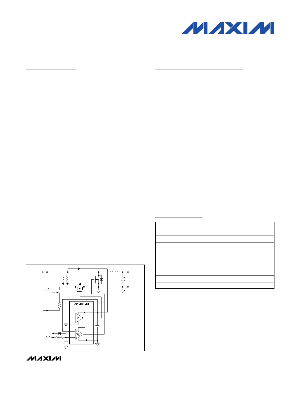
MAX5054
INA+
INA-
INB+
INB-
OUTB
OUTA
V
DD
GND
PWM IN
V
OUT
V
IN
Typical Operating Circuit
19-3348; Rev 0; 8/04
For pricing, delivery, and ordering information, please contact Maxim/Dallas Direct! at
1-888-629-4642, or visit Maxim’s website at www.maxim-ic.com.
*EP = Exposed pad. Package code S8E-14.
Selector Guide and Pin Configurations appear at end of
data sheet.
PART TEMP RANGE
MAX5054AATA -40°C to +125°C 8 TDFN-EP* AGS
MAX5054BATA -40°C to +125°C 8 TDFN-EP* AGR
MAX5055AASA -40°C to +125°C 8 SO-EP* —
MAX5055BASA -40°C to +125°C 8 SO —
MAX5056AASA -40°C to +125°C 8 SO-EP* —
MAX5056BASA -40°C to +125°C 8 SO —
MAX5057AASA -40°C to +125°C 8 SO-EP* —
MAX5057BASA -40°C to +125°C 8 SO —
PINPACKAGE
TOP
MARK
Page 2
4A, 20ns, Dual MOSFET Drivers
2 _______________________________________________________________________________________
ABSOLUTE MAXIMUM RATINGS
ELECTRICAL CHARACTERISTICS
(VDD= 4V to 15V, TA= -40°C to +125°C, unless otherwise noted. Typical values are at VDD= 15V and TA= +25°C.) (Note 1)
Stresses beyond those listed under “Absolute Maximum Ratings” may cause permanent damage to the device. These are stress ratings only, and functional
operation of the device at these or any other conditions beyond those indicated in the operational sections of the specifications is not implied. Exposure to
absolute maximum rating conditions for extended periods may affect device reliability.
(Voltages referenced to GND.)
V
DD
...............................................................................-0.3V to +18V
INA+, INA-, INB+, INB- ...............................................-0.3V to +18V
OUTA, OUTB...................................................-0.3V to (V
DD
+ 0.3V)
OUTA, OUTB Short-Circuit Duration ........................................10ms
Continuous Source/Sink Current at OUT_ (P
D
< P
DMAX
) .....200mA
Continuous Power Dissipation (T
A
= +70°C)
8-Pin TDFN-EP (derate 24.4mW/°C above +70°C)........1951mW
Junction-to-Case Thermal Resistance (θ
JC
) ......................2°C/W
8-Pin SO-EP (derate 19.2mW/°C above +70°C)… ........1538mW
Junction-to-Case Thermal Resistance (θ
JC
) ......................6°C/W
8-Pin SO (derate 5.9mW/°C above +70°C)… ..................471mW
Junction-to-Case Thermal Resistance (θ
JC
) ....................40°C/W
Operating Temperature Range..............................-40°C to +125°C
Storage Temperature Range .................................-65°C to +150°C
Junction Temperature ...........................................................+150°C
Lead Temperature (soldering, 10s)......................................+300°C
MAX5054–MAX5057
POWER SUPPLY
V
DD
VDD Undervoltage Lockout UVLO VDD rising 3.00 3.50 3.85 V
VDD Undervoltage Lockout
Hysteresis
VDD Undervoltage Lockout to
Output Delay
PARAMETER SYMBOL CONDITIONS MIN TYP MAX UNITS
Operating Range V
DD
rising 12 µs
V
DD
415V
200 mV
I
DD
VDD Supply Current
I
DD-SW
DRIVER OUTPUT (SINK)
Driver Output Resistance Pulling
Down
Peak Output Current (Sinking) I
R
ON-N
PK-N
Output-Voltage Low I
Latchup Protection I
LUP
DRIVER OUTPUT (SOURCE)
Driver Output Resistance Pulling
Up
Peak Output Current (Sourcing) I
R
ON-P
PK-P
INA- = INB- = VDD,
VDD = 4V 28 55
INA+ = INB+ = 0V
V
(not switching)
= 15V 40 75
DD
INA- = 0V, INB+ = VDD = 15V,
INA+ = INB- both channels switching at
250kHz, C
VDD = 15V,
I
OUT_
VDD = 4.5V,
I
OUT_
= 0
L
= -100mA
= -100mA
TA = +25°C 1.1 1.8
T
= +125°C 1.5 2.4
A
TA = +25°C 2.2 3.3
T
= +125°C 3.0 4.5
A
1 2.4 4 mA
VDD = 15V, CL = 10,000pF 4 A
= -100mA
OUT_
Reverse current I
VDD = 15V,
I
= 100mA
OUT_
VDD = 4.5V,
I
= 100mA
OUT_
OUT_
VDD = 4.5V 0.45
V
= 15V 0.24
DD
(Note 2) 400 mA
TA = +25°C 1.5 2.1
T
= +125°C 1.9 2.75
A
TA = +25°C 2.75 4
T
= +125°C 3.75 5.5
A
VDD = 15V, CL = 10,000pF 4 A
µA
Ω
V
Ω
Page 3
MAX5054–MAX5057
4A, 20ns, Dual MOSFET Drivers
_______________________________________________________________________________________ 3
ELECTRICAL CHARACTERISTICS (continued)
(VDD= 4V to 15V, TA= -40°C to +125°C, unless otherwise noted. Typical values are at VDD= 15V and TA= +25°C.) (Note 1)
Output-Voltage High I
LOGIC INPUT (Note 3)
Logic 1 Input Voltage V
Logic-Input Hysteresis V
Logic-Input-Current Leakage INA+, INB+, INA-, INB- = 0V or V
Input Capacitance C
SWITCHING CHARACTERISTICS FOR VDD = 15V (Figure 1)
OUT_ Fall Time t
Turn-On Delay Time t
Turn-Off Delay Time t
SWITCHING CHARACTERISTICS FOR VDD = 4.5V (Figure 1)
OUT_ Fall Time t
Turn-On Delay Time t
Turn-Off Delay Time t
PARAMETER SYMBOL CONDITIONS MIN TYP MAX UNITS
V
-
DD
0.55
V
-
DD
0.275
0.7 x
V
DD
2.1
0.3 x
V
DDLogic 0 Input Voltage V
0.1 x
V
DD
-1 +0.1 +1 µA
2.5 pF
IH
IL
HYS
IN
R
F
D-ON
D-OFF
R
F
D-ON
D-OFF
VDD = 4.5V
= 100mA
OUT_
V
= 15V
DD
MAX5054A
MAX5054B/MAX5055/MAX5056/MAX5057
(Note 4)
MAX5054A
MAX5054B/MAX5055/MAX5056/MAX5057 0.8
MAX5054A
MAX5054B/MAX5055/MAX5056/MAX5057 0.3
DD
CL = 1000pF 4
CL = 5000pF 18OUT_ Rise Time t
CL = 10,000pF 32
CL = 1000pF 4
CL = 5000pF 15
CL = 10,000pF 26
CL = 10,000pF (Note 2) 10 20 34 ns
CL = 10,000pF (Note 2) 10 20 34 ns
CL = 1000pF 7
CL = 5000pF 37OUT_ Rise Time t
CL = 10,000pF 85
CL = 1000pF 7
CL = 5000pF 30
CL = 10,000pF 75
CL = 10,000pF (Note 2) 18 35 70 ns
CL = 10,000pF (Note 2) 18 35 70 ns
V
V
V
V
ns
ns
ns
ns
Page 4
MAX5054–MAX5057
4A, 20ns, Dual MOSFET Drivers
4 _______________________________________________________________________________________
ELECTRICAL CHARACTERISTICS (continued)
(VDD= 4V to 15V, TA= -40°C to +125°C, unless otherwise noted. Typical values are at VDD= 15V and TA= +25°C.) (Note 1)
Note 1: All devices are 100% tested at TA= +25°C. Specifications over -40°C to +125°C are guaranteed by design.
Note 2: Limits are guaranteed by design, not production tested.
Note 3: The logic-input thresholds are tested at V
DD
= 4V and VDD= 15V.
Note 4: TTL compatible with reduced noise immunity.
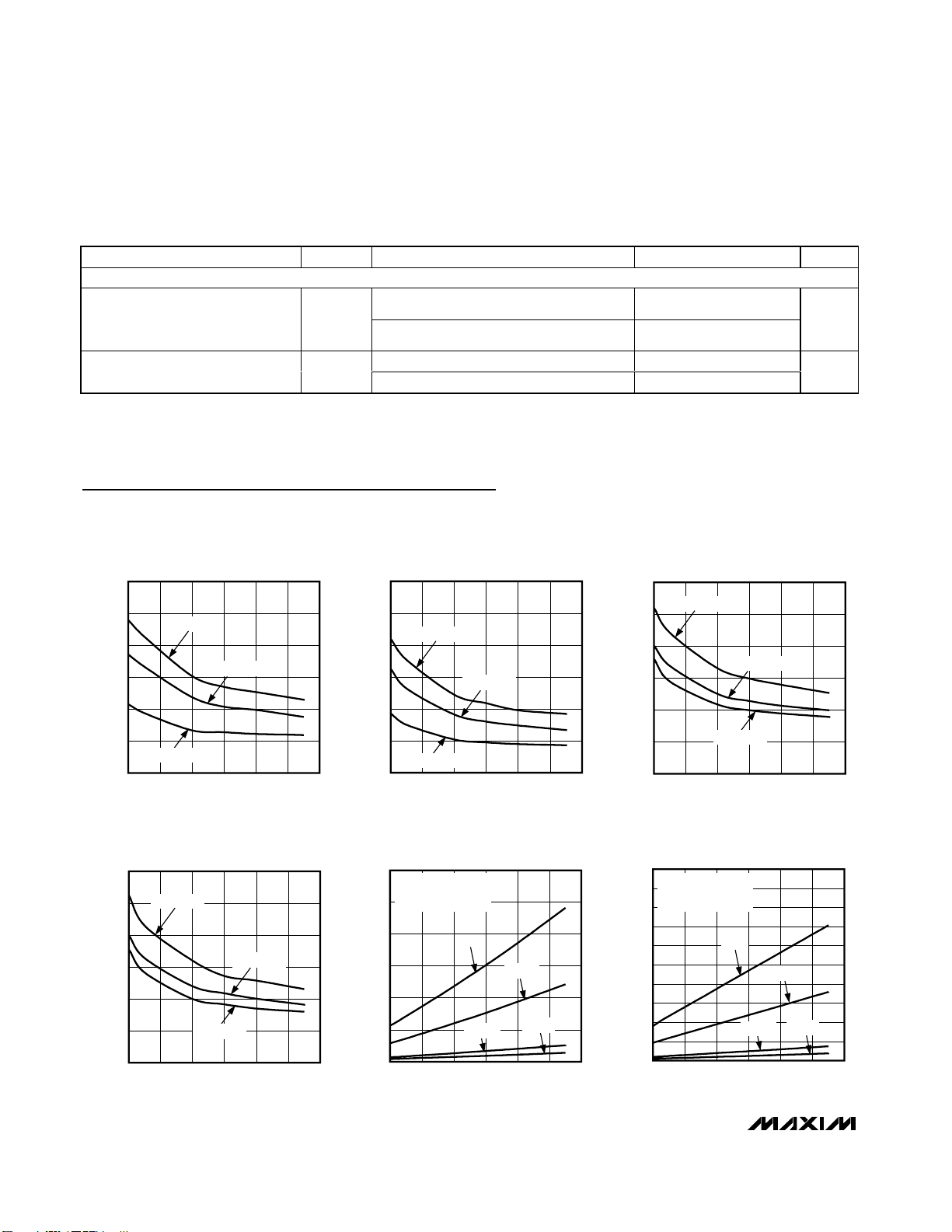
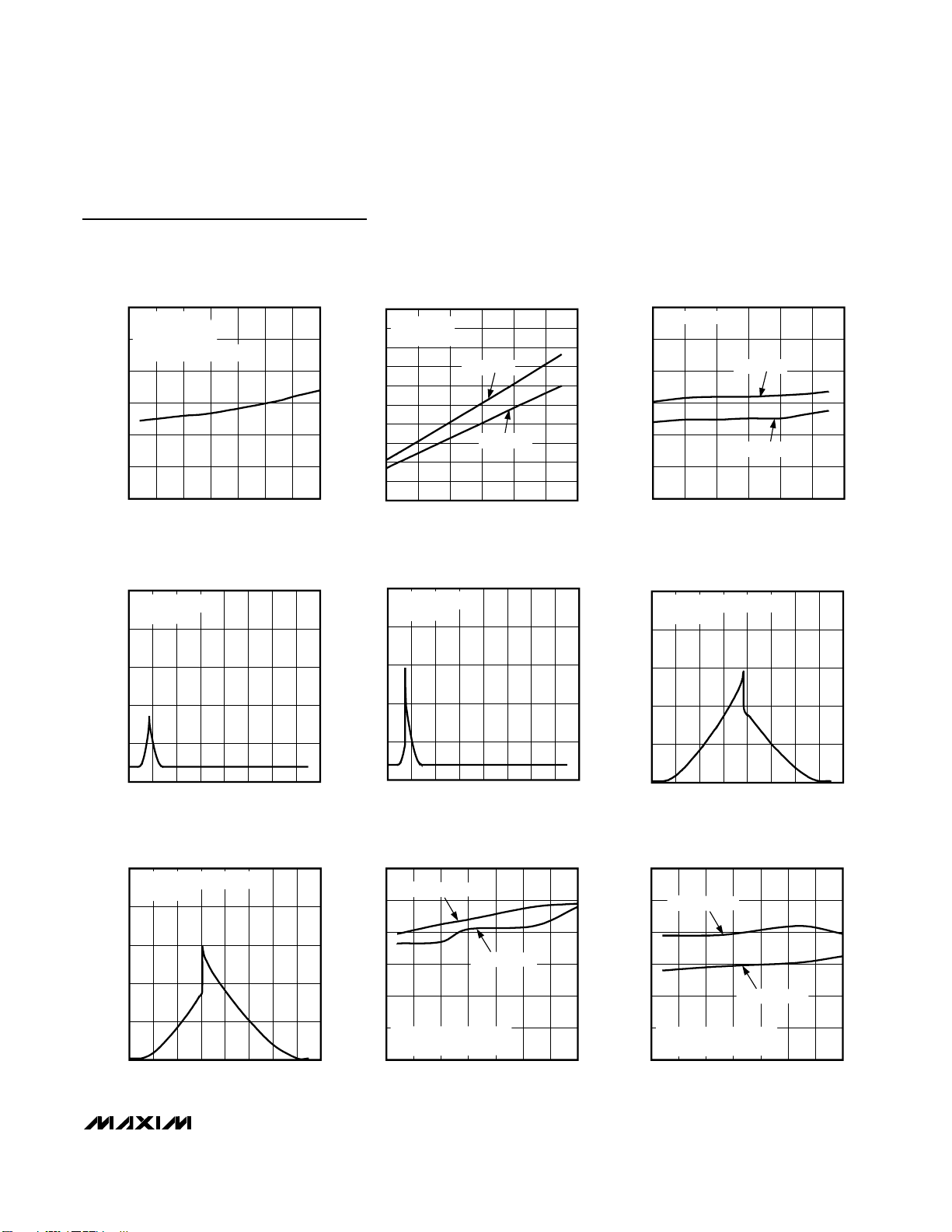
RISE TIME vs. SUPPLY VOLTAGE
(C
L
= 5000pF)
MAX5054 toc01
SUPPLY VOLTAGE (V)
RISE TIME (ns)
14121086
10
20
30
40
50
60
0
416
TA = +125°C
TA = +25°C
TA = -40°C
FALL TIME vs. SUPPLY VOLTAGE
(C
L
= 5000pF)
MAX5054 toc02
TA = +125°C
TA = +25°C
TA = -40°C
FALL TIME (ns)
10
20
30
40
50
60
0
SUPPLY VOLTAGE (V)
14121086416
PROPAGATION DELAY TIME,
LOW-TO-HIGH vs. SUPPLY VOLTAGE
(C
L
= 5000pF)
MAX5054 toc03
TA = +125°C
TA = +25°C
TA = -40°C
PROPAGATION DELAY (ns)
10
20
30
40
50
60
0
SUPPLY VOLTAGE (V)
14121086416
MAX5054 toc04
PROPAGATION DELAY TIME,
HIGH-TO-LOW vs. SUPPLY VOLTAGE
(C
L
= 5000pF)
TA = +125°C
TA = +25°C
TA = -40°C
PROPAGATION DELAY (ns)
10
20
30
40
50
60
0
SUPPLY VOLTAGE (V)
14121086416
I
DD-SW
SUPPLY CURRENT
vs. SUPPLY VOLTAGE
MAX5054 toc05
SUPPLY VOLTAGE (V)
I
DD-SW
SUPPLY CURRENT (mA)
14121086
1
2
3
4
5
6
0
416
DUTY CYCLE = 50%
V
DD
= 15V, CL = 0
1 CHANNEL SWITCHING
1MHz
50kHz
100kHz
500kHz
SUPPLY CURRENT vs. SUPPLY VOLTAGE
MAX5054 toc06
SUPPLY VOLTAGE (V)
SUPPLY CURRENT (mA)
14121086
10
20
30
40
50
60
70
80
90
100
0
416
DUTY CYCLE = 50%
V
DD
= 15V, CL = 4700pF
1 CHANNEL SWITCHING
1MHz
50kHz
100kHz
500kHz
Typical Operating Characteristics
(TA = +25°C, unless otherwise noted.)
MATCHING CHARACTERISTICS
Mismatch Propagation Delays from
Inverting and Noninverting Inputs
to Output
Mismatch Propagation Delays
Between Channel A and Channel B
PARAMETER SYMBOL CONDITIONS MIN TYP MAX UNITS
VDD = 15V, CL = 10,000pF 2
∆t
ON-OFF
VDD = 4.5V, CL = 10,000pF 4
∆t
VDD = 15V, CL = 10,000pF 1
A-B
VDD = 4.5V, CL = 10,000pF 2
ns
ns
Page 5
MAX5054–MAX5057
4A, 20ns, Dual MOSFET Drivers
_______________________________________________________________________________________ 5
Typical Operating Characteristics (continued)
(TA = +25°C, unless otherwise noted.)
I
SUPPLY CURRENT
DD-SW
vs. TEMPERATURE
4.0
VDD = 15V,
f = 250kHz, C
3.5
DUTY CYCLE = 50%
BOTH CHANNELS SWITCHING
3.0
2.5
2.0
SUPPLY CURRENT (mA)
1.5
1.0
-50 125
= 0
L
TEMPERATURE (°C)
1007550250-25
SUPPLY CURRENT vs. LOGIC-INPUT
VOLTAGE (INPUT LOW-TO-HIGH)
500
TTL INPUT VERSIONS
= 15V
V
DD
400
300
INPUT THRESHOLD VOLTAGE
10
MAX5054AATA
9
MAX5054 toc07
(CMOS INPUT)
8
7
6
5
4
3
INPUT THRESHOLD VOLTAGE (V)
2
1
0
416
SUPPLY CURRENT vs. LOGIC-INPUT
VOLTAGE (INPUT HIGH-TO-LOW)
500
TTL INPUT VERSIONS
= 15V
V
MAX5054 toc10
DD
400
300
vs. SUPPLY VOLTAGE
VIN RISING
VIN FALLING
SUPPLY VOLTAGE (V)
3.0
2.5
MAX5054 toc08
2.0
1.5
1.0
INPUT THRESHOLD VOLTAGE (V)
0.5
14121086
MAX5054 toc11
INPUT THRESHOLD VOLTAGE
vs. SUPPLY VOLTAGE
TTL INPUT VERSIONS
VIN RISING
VIN FALLING
0
416
SUPPLY VOLTAGE (V)
SUPPLY CURRENT vs. LOGIC-INPUT
VOLTAGE (INPUT LOW-TO-HIGH)
5
MAX5054AATA (CMOS INPUT)
= 15V
V
DD
4
3
MAX5054 toc09
14121086
MAX5054 toc12
200
SUPPLY CURRENT (µA)
100
0
016
LOGIC-INPUT VOLTAGE (V)
1412108642
SUPPLY CURRENT vs. LOGIC-INPUT
VOLTAGE (INPUT HIGH-TO-LOW)
5
MAX5054AATA (CMOS INPUT)
= +15V
V
DD
4
3
2
SUPPLY CURRENT (mA)
1
0
016
LOGIC-INPUT VOLTAGE (V)
1412108642
200
SUPPLY CURRENT (µA)
100
MAX5054 toc13
-2
DELAY MISMATCH (ns)
-4
-6
0
016
LOGIC-INPUT VOLTAGE (V)
DELAY MISMATCH BETWEEN IN_+
AND IN_- TO OUT_ vs. TEMPERATURE
6
OUTPUT FALLING
4
2
0
MAX5054AATA (CMOS INPUT)
= 4.5V, CL = 10,000pF
V
DD
-50 125
OUTPUT RISING
TEMPERATURE (°C)
2
SUPPLY CURRENT (mA)
1
1412108642
0
016
LOGIC-INPUT VOLTAGE (V)
1412108642
DELAY MISMATCH BETWEEN IN_+
AND IN_- TO OUT_ vs. TEMPERATURE
6
4
MAX5054 toc14
1007550250-25
OUTPUT RISING
2
0
-2
DELAY MISMATCH (ns)
-4
MAX5054AATA (CMOS INPUT)
= 15V, CL = 10,000pF
V
DD
-6
-50 125
OUTPUT FALLING
TEMPERATURE (°C)
MAX5054 toc15
1007550250-25
Page 6
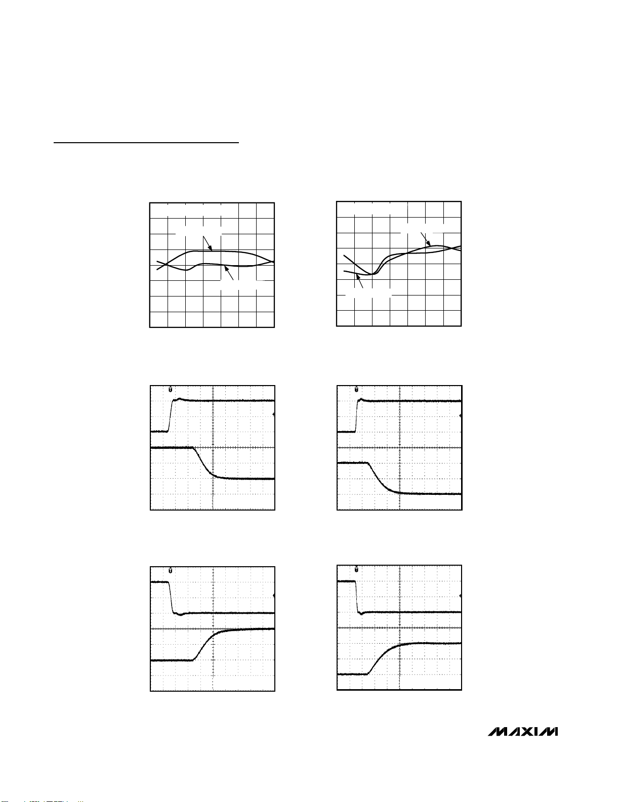
MAX5054–MAX5057
4A, 20ns, Dual MOSFET Drivers
6 _______________________________________________________________________________________
Typical Operating Characteristics (continued)
(TA = +25°C, unless otherwise noted.)
MAX5054 toc16
TEMPERATURE (°C)
DELAY MISMATCH (ns)
10075-25 0 25 50
-3
-2
-1
0
1
2
3
4
-4
-50 125
DELAY MISMATCH BETWEEN 2 CHANNELS
vs. TEMPERATURE
VDD = 4.5V, CL = 10,000pF
OUTPUT RISING
OUTPUT FALLING
MAX5054 toc17
TEMPERATURE (°C)
DELAY MISMATCH (ns)
10075-25 0 25 50
-3
-2
-1
0
1
2
3
4
-4
-50 125
DELAY MISMATCH BETWEEN 2 CHANNELS
vs. TEMPERATURE
VDD = 15V, CL = 10,000pF
OUTPUT RISING
OUTPUT FALLING
LOGIC-INPUT VOLTAGE vs. OUTPUT VOLTAGE
(V
DD
= 4V, CL = 5000pF)
MAX5054 toc18
IN_2V/div
20ns/div
OUT_
2V/div
MAX5055 (TTL INPUT)
MAX5054 toc19
40ns/div
LOGIC-INPUT VOLTAGE vs. OUTPUT VOLTAGE
(V
DD
= 4V, CL = 10,000pF)
IN_2V/div
OUT_
2V/div
MAX5055 (TTL INPUT)
MAX5054 toc20
20ns/div
LOGIC-INPUT VOLTAGE vs. OUTPUT VOLTAGE
(V
DD
= 4V, CL = 5000pF)
IN_2V/div
OUT_
2V/div
MAX5055 (TTL INPUT)
MAX5054 toc21
40ns/div
LOGIC-INPUT VOLTAGE vs. OUTPUT VOLTAGE
(V
DD
= 4V, CL = 10,000pF)
IN_2V/div
OUT_
2V/div
MAX5055 (TTL INPUT)
Page 7

MAX5054–MAX5057
4A, 20ns, Dual MOSFET Drivers
_______________________________________________________________________________________ 7
Typical Operating Characteristics (continued)
(TA = +25°C, unless otherwise noted.)
LOGIC-INPUT VOLTAGE vs. OUTPUT VOLTAGE
= 15V, CL = 5000pF)
(V
DD
LOGIC-INPUT VOLTAGE vs. OUTPUT VOLTAGE
= 15V, CL = 5000pF)
(V
DD
20ns/div
MAX5054 toc22
MAX5055
MAX5054 toc24
IN_2V/div
OUT_
5V/div
IN_2V/div
LOGIC-INPUT VOLTAGE vs. OUTPUT VOLTAGE
LOGIC-INPUT VOLTAGE vs. OUTPUT VOLTAGE
= 15V, CL = 10,000pF)
(V
DD
40ns/div
= 15V, CL = 10,000pF)
(V
DD
MAX5054 toc23
MAX5055
MAX5054 toc25
IN_2V/div
OUT_
5V/div
IN_2V/div
MAX5054 toc27
OUT_
5V/div
V
DD
5V/div
OUTA
5V/div
OUTB
5V/div
MAX5055
20ns/div
VDD vs. OUTPUT VOLTAGE
MAX5055
INA- = INB- = GND
= CLB = 10,000pF
C
LA
2ms/div
MAX5054 toc26
OUT_
5V/div
V
DD
5V/div
OUTA
5V/div
OUTB
5V/div
MAX5055
40ns/div
VDD vs. OUTPUT VOLTAGE
MAX5055
INA- = INB- = GND
= CLB = 10,000pF
C
LA
2ms/div
Page 8

MAX5054–MAX5057
4A, 20ns, Dual MOSFET Drivers
8 _______________________________________________________________________________________
Pin Descriptions
MAX5054
MAX5055/MAX5056/MAX5057
PIN NAME FUNCTION
1 INA- Inverting Logic-Input Terminal for Driver A. Connect to GND when not used.
2 INB- Inverting Logic-Input Terminal for Driver B. Connect to GND when not used.
3 GND Ground
4 OUTB Driver B Output. Sources or sinks current for channel B to turn the external MOSFET on or off.
5VDDPower Supply. Bypass to GND with one or more 0.1µF ceramic capacitors.
6 OUTA Driver A Output. Sources or sinks current for channel A to turn the external MOSFET on or off.
7 INB+ Noninverting Logic-Input Terminal for Driver B. Connect to VDD when not used.
8 INA+ Noninverting Logic-Input Terminal for Driver A. Connect to VDD when not used.
—EP
MAX5055 MAX5056 MAX5057
1, 8 1, 8 1, 8 N.C. No Connection. Not internally connected.
2 — 2 INA- Inverting Logic-Input Terminal for Driver A. Connect to GND if not used.
3 3 3 GND Ground
4 — — INB- Inverting Logic-Input Terminal for Driver B. Connect to GND if not used.
5 5 5 OUTB
666VDDPower Supply. Bypass to GND with one or more 0.1µF ceramic capacitors.
7 7 7 OUTA
— 4 4 INB+ Noninverting Logic-Input Terminal for Driver B. Connect to VDD if not used.
— 2 — INA+ Noninverting Logic-Input Terminal for Driver A. Connect to VDD if not used.
———EP
PIN
Exposed Pad. Internally connected to GND. Do not use the exposed pad as the only electrical
ground connection.
NAME FUNCTION
Driver B Output. Sources or sinks current for channel B to turn the external
MOSFET on or off.
Driver A Output. Sources or sinks current for channel A to turn the external
MOSFET on or off.
Exposed Pad. Internally connected to GND. Do not use the exposed pad as
the only electrical ground connection.
Page 9

Detailed Description
VDDUndervoltage Lockout (UVLO)
The MAX5054–MAX5057 have internal undervoltage
lockout for VDD. When VDDis below the UVLO threshold, OUT_ is low, independent of the state of the inputs.
The undervoltage lockout is typically 3.5V with 200mV
typical hysteresis to avoid chattering. When VDDrises
above the UVLO threshold, the outputs go high or low
depending upon the logic-input levels. Bypass V
DD
using low-ESR ceramic capacitors for proper operation
(see the Applications Information section).
Logic Inputs
The MAX5054B–MAX5057 have TTL-compatible logic
inputs, while the MAX5054A is a CMOS logic-input driver. The logic-input signals can be independent of the
VDDvoltage. For example, the device can be powered
by a 5V supply while the logic inputs are provided from
CMOS logic. Also, the logic inputs are protected against
the voltage spikes up to 18V, regardless of the VDDvoltage. The TTL and CMOS logic inputs have 300mV and
0.1 x VDDhysteresis, respectively, to avoid possible double pulsing during transition. The low 2.5pF input capacitance reduces loading and increases switching speed.
MAX5054–MAX5057
4A, 20ns, Dual MOSFET Drivers
_______________________________________________________________________________________ 9
Figure 1. Timing Diagram
Figure 2. MAX5054 Block Diagram (1 Driver)
Figure 3. MAX5055/MAX5056/MAX5057 Functional Diagrams
(1 Driver)
IN_+
V
IL
OUT_
t
D-OFF1
V
IH
IN_-
t
D-OFF2
RISING MISMATCH = t
FALLING MISMATCH = t
D-ON2
D-OFF2
- t
D-ON1
- t
MAX5054
IN_-
IN_+
D-OFF1
t
F
V
IL
V
BREAK-
BEFORE-
MAKE
CONTROL
IH
V
DD
P
OUT_
N
GND
V
DD
t
D-ON1
t
D-ON2
90%
10%
MAX5055
MAX5056
MAX5057
BREAK-
t
R
IN_+
NONINVERTING INPUT DRIVER
BEFORE-
MAKE
CONTROL
MAX5055
V
DD
P
OUT_
N
IN_-
MAX5056
MAX5057
BREAK-
BEFORE-
MAKE
CONTROL
P
OUT_
N
GND
GND
INVERTING INPUT DRIVER
Page 10

MAX5054–MAX5057
The logic inputs are high impedance and must not be left
floating. If the inputs are left open, OUT_ can go to an
undefined state as soon as VDDrises above the UVLO
threshold. Therefore, the PWM output from the controller
must assume proper state when powering up the device.
The MAX5054 has two logic inputs per driver providing
greater flexibility in controlling the MOSFET. Use IN_+ for
noninverting logic and IN_- for inverting logic operation.
Connect IN_+ to VDDand IN_- to GND if not used.
Alternatively, the unused input can be used as an
ON/OFF function. Use IN_+ for active-low shutdown logic
and IN_- for active-high shutdown logic (see Figure 4).
See Table 1 for all possible input combinations.
Driver Output
The MAX5054–MAX5057 have low R
DS(ON)
p-channel
and n-channel devices (totem pole) in the output stage
for the fast turn-on and turn-off high gate-charge switching MOSFETs. The peak source or sink current is typically
4A. The OUT_ voltage is approximately equal to V
DD
when in high state and is ground when in low state. The
driver R
DS(ON)
is lower at higher VDD, thus higher
source-/sink-current capability and faster switching
speeds. The propagation delays from the noninverting
and inverting logic inputs to outputs are matched to 2ns.
The break-before-make logic avoids any cross-conduction between the internal p- and n-channel devices, and
eliminates shoot-through currents reducing the quiescent
supply current.
Applications Information
RLC Series Circuit
The driver’s R
DS(ON)(RON
), internal bond and lead
inductance (LP), trace inductance (LS), gate inductance
(L
G
), and gate capacitance (CG) form a series RLC
circuit with a second-order characteristic equation. The
series RLC circuit has an undamped natural frequency
(ϖ0) and a damping ratio (ζ) where:
The damping ratio needs to be greater than 0.5 (ideally 1)
to avoid ringing. Add a small resistor (R
GATE
) in series
with the gate when driving a very low gate-charge
MOSFET, or when the driver is placed away from the
MOSFET. Use the following equation to calculate the
series resistor:
L
P
can be approximated as 3nH and 2nH for SO and
TDFN packages, respectively. LSis on the order of
20nH/in. Verify LGwith the MOSFET vendor.
4A, 20ns, Dual MOSFET Drivers
10 ______________________________________________________________________________________
Figure 4. Unused Input as an ON/OFF Function (1/2 MAX5054A)
Table 1. MAX5054 Truth Table
Table 2. MAX5055/MAX5056/MAX5057
Truth Table
INA+/INB+ INA-/INB- OUTA/OUTB
Low Low Low
Low High Low
High Low High
High High Low
IN_+ OUT_
Low Low
High High
IN_- OUT_
Low High
High Low
NONINVERTING
INVERTING
V
DD
PWM
INPUT
OFF
ON
MAX5054A
INA+ OUTA
INA-
GND
ϖ
=
0
ξ
=
2
R
GATE
()
LLL C
×
≥
1
++ ×
PSG G
R
ON
++
()
LLL
PSG
C
G
LLL
++
()
PSG
C
G
R
−
ON
Page 11

Supply Bypassing and Grounding
Pay extra attention to bypassing and grounding the
MAX5054–MAX5057. Peak supply and output currents
may exceed 8A when both drivers drive large external
capacitive loads in phase. Supply voltage drops and
ground shifts create forms of negative feedback for
inverters and may degrade the delay and transition times.
Ground shifts due to insufficient device grounding may
also disturb other circuits sharing the same AC ground
return path. Any series inductance in the V
DD
, OUT_,
and/or GND paths can cause oscillations due to the very
high di/dt when switching the MAX5054–MAX5057 with
any capacitive load. Place one or more 0.1µF ceramic
capacitors in parallel as close to the device as possible to
bypass V
DD
to GND. Use a ground plane to minimize
ground return resistance and series inductance. Place
the external MOSFET as close as possible to the
MAX5054–MAX5057 to further minimize board inductance and AC path impedance.
Power Dissipation
Power dissipation of the MAX5054–MAX5057 consists
of three components: caused by the quiescent current,
capacitive charge/discharge of internal nodes, and the
output current (either capacitive or resistive load).
Maintain the sum of these components below the maximum power dissipation limit.
The current required to charge and discharge the internal
nodes is frequency dependent (see the Supply Current
vs. Supply Voltage graph in the Typical Operating
Characteristics). The power dissipation (PQ) due to the
quiescent switching supply current (I
DD-SW
) per driver
can be calculated as:
P
Q
= VDDx I
DD-SW
For capacitive loads, use the following equation to estimate the power dissipation per driver:
P
CLOAD
= C
LOAD
x (VDD)2x f
SW
where C
LOAD
is the capacitive load, VDDis the supply
voltage, and fSWis the switching frequency.
Calculate the total power dissipation (PT) per driver as
follows:
PT= PQ+ P
CLOAD
Use the following equation to estimate the MAX5054–
MAX5057 total power dissipation per driver when driving
a ground-referenced resistive load:
PT= PQ+ P
RLOAD
P
RLOAD
= D x R
ON(MAX)
x I
LOAD
2
where D (duty cycle) is the fraction of the period the
MAX5054–MAX5057’s output pulls high duty cycle,
R
ON(MAX)
is the maximum on-resistance of the device
with the output high, and I
LOAD
is the output load current
of the MAX5054–MAX5057.
Layout Information
The MAX5054–MAX5057 MOSFET drivers source and
sink large currents to create very fast rising and falling
edges at the gate of the switching MOSFET. The high
di/dt can cause unacceptable ringing if the trace
lengths and impedances are not well controlled. Use the
following PC board layout guidelines when designing
with the MAX5054–MAX5057:
• Place one or more 0.1µF decoupling ceramic
capacitors from VDDto GND as close to the device
as possible. Connect VDDand GND to large copper
areas. Place one bulk capacitor of 10µF (min) on
the PC board with a low resistance path to the V
DD
input and GND of the MAX5054–MAX5057.
• Two AC current loops form between the device and
the gate of the driven MOSFET. The MOSFET looks
like a large capacitance from gate to source when the
gate pulls low. The active current loop is from the
MOSFET gate to OUT_ of the MAX5054–MAX5057, to
GND of the MAX5054–MAX5057, and to the source of
the MOSFET. When the gate of the MOSFET pulls
high, the active current is from the VDDterminal of the
decoupling capacitor, to VDDof the MAX5054–
MAX5057, to OUT_ of the MAX5054–MAX5057, to the
MOSFET gate, to the MOSFET source, and to the
negative terminal of the decoupling capacitor. Both
charging current and discharging current loops are
important. Minimize the physical distance and the
impedance in these AC current paths.
• Keep the device as close to the MOSFET as possible.
• In a multilayer PC board, the inner layers should
consist of a GND plane containing the discharging
and charging current loops.
• Pay extra attention to the ground loop and use a
low-impedance source when using a TTL logicinput device. Fast fall time at OUT_ may corrupt the
input during transition.
MAX5054–MAX5057
4A, 20ns, Dual MOSFET Drivers
______________________________________________________________________________________ 11
Page 12

MAX5054–MAX5057
Exposed Pad
Both the SO-EP and TDFN-EP packages have an
exposed pad on the bottom of their package. These
pads are internally connected to GND. For the best
thermal conductivity, solder the exposed pad to the
ground plane to dissipate 1.5W and 1.9W in SO-EP and
TDFN-EP packages, respectively. Do not use the
ground-connected pads as the only electrical ground
connection or ground return. Use GND (pin 3) as the
primary electrical ground connection.
4A, 20ns, Dual MOSFET Drivers
12 ______________________________________________________________________________________
Additional Application Circuits
Figure 5. Push-Pull Converter with Synchronous Rectification Drive Using MAX5054
V
IN
PWM IN
MAX5054
INA+
INA-
V
OUTA
V
DD
DD
PWM IN
V
OUT
MAX5054
V
INA+
INA-
INB+
INB-
DD
OUTA
OUTB
GND
PWM IN
INB+
OUTB
INB-
GND
Page 13

MAX5054–MAX5057
4A, 20ns, Dual MOSFET Drivers
______________________________________________________________________________________ 13
Figure 6. Schematic of a 48V Input, 3.3V at 15A Output Synchronously Rectified, Isolated Power Supply
R21
REG5
XFRMRH
R4
1%
24.9kΩ
1MΩ
28
SYNCIN
RCOSC
1
IN
+V
IN
+V
1%
U1
C1
100pF
IN
-V
IN
+V
C25
0.047µF
C12
1µF
C11
0.47µF
C10
0.47µF
6
7
8
N1
2
1
3
D2
21
R6
C7
0.22µF
27
FLTINT
MAX5051
IN
+V
100V
100V
100V
100V
5
4
R5
1MΩ
SYNCOUT
2
TP1
R25
R29
XFRMRH
3
5V
C35
1%
38.3kΩ
1%
26
STARTUP ON/OFF
RCFF
3
100kΩ
1µF
25
C2
DRVB
1Ω
1
2
N5
C16
3.3µF
6
8
7
WDI
N.C.
U5
IN OUT
EN
3
1
2
C32
1µF
D6
21
REG9
R7
0Ω
2
D1
C8
IN
+V
24
23
GND
AVIN
UVLO
CSS4COM6COMP7FB8REG5
5
C5
390pF
D8
OUT
V
5
HOLD
L1
GND
RESET
4
R13
R8
4.7µF
22
21
20
BST
DRVH
R15
31.6kΩ
4700pF
R16
10.5kΩ
21
2.4µH
XFRMRH
47Ω
8.2Ω
XFRMRH
19
XFRMRH
1%
1%
VOUT
C33
C15
C14
C13
6
5
8
2
DRVB
DRVB
REG5
C4
1
T1
7
C34
REG9
4.7µF
1µF
270µF
270µF
270µF
N4
D4
18
10V
4V
4V
4V
3
2
R10
8
8T
330pF
+VIN
DRVDD
REG9
C3
SGND
4
1
2
20Ω
5
D3
C9
9
4.7µF
C23
2T
1
8
7
5
6
12
R9
1µF
17
PGND
REG9
PVIN
C6
R26
560Ω
LXH
1
AN
CC
V
5
5V
C31
0.1µF
8
INA+
U4
OUTA
6
N3
6
5
1000pF
7
8
1
10
D7
6
4T
D5
1
2
3
2
N2
1
R17
4
8.2Ω
R14
C20
220pF
16CS15
DRVL
PVIN
STT12LXVDD13LXH
10
11
C18
1000pF
0.1µF
REG5
U6
4
3
2
0.027Ω
270Ω
R28
2kΩ
OUT
4
2
INB-
MAX5054
OUTB
4
1
2
R18
4.7Ω
1%
29
C19
1µF
R27
10Ω
2
CA
GND
3
IC_PADDLE
U1: MAX5051
U2: PS2913-1-M
U3: MAX8515
U4: MAX5054
U5: MAX5023M
U6: PS9715
N1, N2: SI4486
N3, N4: SI4864
N5: BSS123
C30
0.1µF
5
3
DD
V
INB+
7
+5V +5V
IN
R22
15kΩ
PVIN +V
OUT
V
C27
R20
LXL
14
TP3
REG5
LXH
C21
GND
INA-
1
80V
4.7µF
0.15µF
0Ω
R19
R12
475Ω
100kΩ
1
U2
4
R3
2.2kΩ
1%
C24
C26
0.1µF
REG9
2kV
C22
2200pF
R24
10Ω
OUT
V
1
4
IN
GND
PGND
U3
OUT
FB
3
52
R2
2.55kΩ
1%
TRIM
R1
1%
11.5kΩ
C28
C17
0.047µF
OUT
V
C36
0.22µF
0.33µF
2
3
R11
1000pF
360Ω
SENSE (+) SENSE (-)
R23
10Ω
Page 14

MAX5054–MAX5057
4A, 20ns, Dual MOSFET Drivers
14 ______________________________________________________________________________________
Chip Information
TRANSISTOR COUNT: 258
PROCESS: CMOS
OUTA
V
DD
OUTB
1
2
87INA+
INB+INB-
GND
INA-
TDFN-EP
TOP VIEW
3
4
6
5
MAX5054
V
DD
OUTBINB-
1
2
87N.C.
OUTAINA-
GND
N.C.
SO/SO-EP
3
4
6
5
MAX5055
V
DD
OUTBINB+
1
2
87N.C.
OUTAINA+
GND
N.C.
SO/SO-EP
3
4
6
5
MAX5056
V
DD
OUTBINB+
1
2
87N.C.
OUTAINA-
GND
N.C.
SO/SO-EP
3
4
6
5
MAX5057
Pin Configurations
Selector Guide
*EP = Exposed pad.
PART
MAX5054AATA 8 TDFN-EP*
MAX5054BATA 8 TDFN-EP*
MAX5055AASA 8 SO-EP* TTL Dual Inverting Inputs
MAX5055BASA 8 SO TTL Dual Inverting Inputs
MAX5056AASA 8 SO-EP* TTL Dual Noninverting Inputs
MAX5056BASA 8 SO TTL Dual Noninverting Inputs
MAX5057AASA 8 SO-EP*
MAX5057BASA 8 SO
PINPACKAGE
LOGIC INPUT
V
/ 2 CMOS Dual Inverting
DD
and Dual Noninverting Inputs
TTL Dual Inverting and Dual
Noninverting Inputs
TTL Inverting and
Noninverting Inputs
TTL Inverting and
Noninverting Inputs
Page 15

MAX5054–MAX5057
4A, 20ns, Dual MOSFET Drivers
______________________________________________________________________________________ 15
Package Information
(The package drawing(s) in this data sheet may not reflect the most current specifications. For the latest package outline information
go to www.maxim-ic.com/packages
.)
N
1
TOP VIEW
D
e
FRONT VIEW
INCHES
DIM
MIN
0.053A
0.004
A1
0.014
B
0.007
C
e 0.050 BSC 1.27 BSC
0.150
HE
A
B
A1
C
L
E
H 0.2440.228 5.80 6.20
0.016L
VARIATIONS:
INCHES
MINDIM
D
0.189 0.197 AA5.004.80 8
0.337 0.344 AB8.758.55 14
D
0∞-8∞
SIDE VIEW
MAX
0.069
0.010
0.019
0.010
0.157
0.050
MAX
0.3940.386D
MILLIMETERS
MAX
MIN
1.35
1.75
0.10
0.25
0.35
0.49
0.19
0.25
3.80 4.00
0.40 1.27
MILLIMETERS
MAX
MIN
9.80 10.00
N MS012
16
AC
SOICN .EPS
PROPRIETARY INFORMATION
TITLE:
PACKAGE OUTLINE, .150" SOIC
REV.DOCUMENT CONTROL NO.APPROVAL
21-0041
1
B
1
Page 16

MAX5054–MAX5057
4A, 20ns, Dual MOSFET Drivers
16 ______________________________________________________________________________________
Package Information (continued)
(The package drawing(s) in this data sheet may not reflect the most current specifications. For the latest package outline information
go to www.maxim-ic.com/packages
.)
8L, SOIC EXP. PAD.EPS
PACKAGE OUTLINE
8L SOIC, .150" EXPOSED PAD
21-0111
1
B
1
Page 17

MAX5054–MAX5057
4A, 20ns, Dual MOSFET Drivers
Maxim cannot assume responsibility for use of any circuitry other than circuitry entirely embodied in a Maxim product. No circuit patent licenses are
implied. Maxim reserves the right to change the circuitry and specifications without notice at any time.
Maxim Integrated Products, 120 San Gabriel Drive, Sunnyvale, CA 94086 408-737-7600 ____________________ 17
© 2004 Maxim Integrated Products Printed USA is a registered trademark of Maxim Integrated Products.
Package Information (continued)
(The package drawing(s) in this data sheet may not reflect the most current specifications. For the latest package outline information
go to www.maxim-ic.com/packages
.)
PIN 1
INDEX
AREA
D
E
A
NUMBER OF LEADS SHOWN ARE FOR REFERENCE ONLY
DETAIL A
L
N
E2
C
L
e
C
L
L
e
PACKAGE OUTLINE, 6, 8, 10 & 14L,
TDFN, EXPOSED PAD, 3x3x0.80 mm
21-0137
6, 8, &10L, DFN THIN.EPS
1
F
2
COMMON DIMENSIONS
MIN. MAX.
SYMBOL
A 0.70 0.80
D 2.90 3.10
E 2.90 3.10
A1 0.00 0.05
L
A2 0.20 REF.
PACKAGE VARIATIONS
PKG. CODE
T833-1
T1033-1
0.40
0.20
0.25 MIN.k
N D2 E2 e
2.30±0.101.50±0.106T633-1 0.95 BSC MO229 / WEEA
1.50±0.10
2.30±0.108
1.50±0.10
1.70±0.10 2.30±0.1014T1433-1
1.70±0.10
0.65 BSC
2.30±0.1010
0.50 BSC
0.40 BSC
0.40 BSC
JEDEC SPEC
MO229 / WEEC
MO229 / WEED-3
- - - - 0.20±0.03 2.40 REFT1433-2 14 2.30±0.10
b
0.40±0.05
[(N/2)-1] x e
1.90 REF
1.95 REF0.30±0.05
2.00 REF0.25±0.05
2.40 REF0.20±0.03- - - -
PACKAGE OUTLINE, 6, 8, 10 & 14L,
TDFN, EXPOSED PAD, 3x3x0.80 mm
21-0137
2
F
2
 Loading...