

Page 1
现货库存、技术资料、百科信息、热点资讯,精彩尽在鼎好!
General Description
The MAX5042/MAX5043 isolated multimode PWM power
ICs feature integrated switching power MOSFETs connected in a voltage-clamped, two-transistor, power-circuit
configuration. These devices operate from a wide 20V to
76V input voltage range. The MAX5042 includes a hotswap controller for use with an external power MOSFET to
limit inrush current for applications where the power supply is plugged into a live power backplane. The MAX5043
does not include a hot-swap controller.
The voltage-clamped power topology of the MAX5042/
MAX5043 enables full recovery of stored magnetizing
and leakage inductive energy for enhanced efficiency
and reliability. Operating at up to 500kHz switching frequency, these devices provide up to 50W of output
power. The MAX5042/MAX5043 allow the implementation of both forward and flyback voltage or current-mode
converter topologies. A dedicated latched external shutdown provides protection in addition to internal thermal
shutdown.
The MAX5042/MAX5043 achieve higher efficiency when
used with secondary-side synchronous rectification.
These devices generate a look-ahead signal for driving
secondary-side synchronous rectifiers.
The MAX5042/MAX5043 are rated for operation over the
-40°C to +125°C and -40°C to +85°C temperature
range, respectively, and are available in a small surfacemount 56-pin thin QFN package.
Warning: The MAX5042/MAX5043 are designed to
work with high voltages. Exercise caution.
Applications
High-Efficiency Telecom/Datacom Power
Supplies
Router/Switch Cards with 48V Backplane Power
Systems
Servers with 48V Backplane Power Systems
xDSL Line Cards
xDSL Line-Driver Power Supplies
Distributed Power Systems with 48V Bus
42V Automotive Power Supplies
Power-Supply Modules
Features
♦ Reliable Single-Stage Clamped Two-Switch Power
ICs for High Efficiency
♦ No Reset Winding Required
♦ Up to 50W Output Power
♦ Integrated High-Voltage 75mΩ Power MOSFETs
♦ 20V to 76V Wide Input Voltage Range
♦ Feed-Forward Voltage or Current-Mode Control
♦ Programmable Brownout Undervoltage Lockout
♦ Integrated Current Signal Amplifier for High-
Efficiency, Current-Mode Control
♦ Internal Overtemperature Shutdown
♦ Indefinite Short-Circuit Protection
♦ Integrated Thermally Protected High-Voltage
Startup Linear Regulator
♦ Integrated Hot-Swap Controller (MAX5042)
♦ Integrated Look-Ahead Signal Output Drives
High-Speed Optocoupler for Secondary-Side
Synchronous Rectification
♦ >90% Efficiency with Synchronous Rectification
♦ Up to 500kHz Switching Frequency
♦ High-Power, Small-Footprint 56-Pin Thermally
Enhanced QFN Package
MAX5042/MAX5043
Two-Switch Power ICs with Integrated
Power MOSFETs and Hot-Swap Controller
________________________________________________________________ Maxim Integrated Products 1
Ordering Information
19-3046; Rev 2; 6/04
For pricing, delivery, and ordering information, please contact Maxim/Dallas Direct! at
1-888-629-4642, or visit Maxim’s website at www.maxim-ic.com.
Pin Configurations appear at end of data sheet.
Selector Guide
EVALUATION KIT
AVAILABLE
PART TEMP RANGE PIN-PACKAGE
MAX5042ATN -40°C to +125°C 56 Thin QFN
MAX5043ETN -40°C to +85°C 56 Thin QFN
PART DESCRIPTION
Two-Switch Power IC with Integrated Power
MAX5042
MAX5043
MOSFETs and Hot-Swap Controller for Isolated
Power Supplies
Two-Switch Power IC with Integrated Power
MOSFETs for Isolated Power Supplies
Page 2
MAX5042/MAX5043
Two-Switch Power ICs with Integrated
Power MOSFETs and Hot-Swap Controller
2 _______________________________________________________________________________________
ABSOLUTE MAXIMUM RATINGS
Stresses beyond those listed under “Absolute Maximum Ratings” may cause permanent damage to the device. These are stress ratings only, and functional
operation of the device at these or any other conditions beyond those indicated in the operational sections of the specifications is not implied. Exposure to
absolute maximum rating conditions for extended periods may affect device reliability.
PWMNEG, POSINPWM, DRNH,
XFRMRH, XFRMRL, SRC to NEGIN....................-0.3V to +80V
BST to NEGIN.........................................................-0.3V to +95V
BST to XFRMRH .....................................................-0.3V to +12V
SRC to PWMNEG .....................................................-0.3V to +6V
REG15 to PWMNEG ...............................................-0.3V to +40V
REG15 to POSINPWM ............................................-80V to +0.3V
REG9, DRVIN to PWMNEG ....................................-0.3V to +12V
REG5 to PWMNEG ...................................................-0.3V to +6V
REG15 Current..................................................................±80mA
REG9 Current......................................................................40mA
REG5 Current......................................................................20mA
UVLO, RAMP, CSS, FLTINT, CSOUT,
RCFF, RCOSC to PWMNEG ...............................-0.3V to +12V
OPTO, PWMSD, SYNC, CSP, CSN,
DRVDEL to PWMNEG...........................................-0.3V to +6V
PPWM to PWMNEG .................................-0.3V to (REG5 + 0.3V)
PPWM Current .................................................................±20mA
PWMPNEG to PWMNEG .......................................-0.3V to +0.3V
DRNH Continuous Average Current (all pins combined)
T
J
= +125°C.........................................................................2A
T
J
= +150°C......................................................................1.4A
XFRMRH Continuous Average Current (all pins combined)
T
J
= +125°C.........................................................................2A
T
J
= +150°C......................................................................1.4A
XFRMRL Continuous Average Current (all pins combined)
T
J
= +125°C.........................................................................2A
T
J
= +150°C......................................................................1.4A
SRC Continuous Current (all pins combined)
T
J
= +125°C.........................................................................2A
T
J
= +150°C......................................................................1.4A
POSINHS to NEGIN................................................-0.3V to +80V
HSEN to NEGIN........................................................-0.3V to +4V
DEN to PWMNEG .....................................................-0.3V to +4V
HSGATE to NEGIN .................................................-0.3V to +12V
HSDRAIN, HSOK to NEGIN....................................-0.3V to +80V
HSOK Current .....................................................................20mA
Continuous Power Dissipation (T
A
= +70°C)
56-Pin Thin QFN (derate 47.6mW/°C above +70°C) .......3.8W
Junction to Ambient Thermal Resistance, θ
JA
...............+21°C/W
Operating Temperature Range
MAX5042ATN ................................................-40°C to +125°C
MAX5043ETN ..................................................-40°C to +85°C
Junction Temperature......................................................+150°C
Storage Temperature Range .............................-65°C to +150°C
Lead Temperature (soldering, 10s) .................................+300°C
(See the Absolute Maximum Ratings Diagram below to better understand the absolute maximum ratings of the various blocks.)
IC SUBSTRATE, NEGIN
PWMNEG,
PWMPNEG,
HSDRAIN,
HSOK
POSINHS,
POSINPWM
REG15
REG9, UVLO, RAMP, CSS, FLTINT,
CSOUT, RCFF, RCOSC, DRVIN
REG5, OPTO, PWMSD, SYNC, CSP,
CSN, DRVDEL, SRC, PPWM
HSEN
HSGATE
XFRMRL
XFRMRH, DRNH
BST
DEN
80V
80V
80V
40V
12V
6V
4V
80V
12V
4V
12V
80V
80V
95V
Absolute Maximum Ratings Diagram
Page 3
_______________________________________________________________________________________ 3
MAX5042/MAX5043
Two-Switch Power ICs with Integrated
Power MOSFETs and Hot-Swap Controller
ELECTRICAL CHARACTERISTICS
(V
POSINPWM
= 20V to 76V, V
REG15
= 18V, C
REG15
= 4.7µF, C
REG9
= 1µF, C
REG5
= 1µF, R
RCOSC
= 24kΩ, C
RCOSC
= 100pF, C
BST
=
0.22µF, R
DRVDEL
= 10kΩ, C
DRVDEL
= 0.22µF, V
CSS
= V
CSP
= V
CSN
= V
RAMP
= V
PWMNEG
= V
NEGIN
= 0, TA= T
MIN
to T
MAX
, unless
otherwise noted. Typical values are at V
POSINPWM
= 48V, TA= +25°C, unless otherwise noted. All voltages are referred to PWMNEG,
unless otherwise noted.)
PARAMETER
SYMBOL
CONDITIONS
MIN
TYP
MAX
UNITS
Input Supply Range
20 76 V
REG15 REGULATOR
REG15 Output Voltage Range
V
POSINPWM
= 20V to 76V
V
REG15 Output Voltage Load
Regulation
V
POSINPWM
= 20V, I
REG15
= 0 to 80mA 1.5 V
REG15 Output Current Inferred from load regulation test 80 mA
REG15 Current Limit REG15 shorted to PWMNEG with 10Ω
mA
REG15 Overdrive Voltage 18 40 V
REG9 REGULATOR
REG9 Output Voltage Range V
REG15
= 18V to 40V 8.3
V
REG9 Output Voltage Load
Regulation
I
REG9
= 0 to 40mA
V
REG9 Output Current Inferred from load regulation test 40 mA
REG9 Current Limit REG9 shorted to PWMNEG with 10Ω
mA
REG5 REGULATOR
REG5 Output Voltage Range V
REG15
= 18V to 40V 4.5 5.5 V
REG5 Output Voltage Load
Regulation
I
REG5
= 0 to 20mA
V
REG5 Output Current Inferred from load regulation test 20 mA
REG5 Current Limit REG5 shorted to PWMNEG with 10Ω 40 mA
PWM COMPARATOR
Common-Mode Range
0 5.5 V
Input Offset Voltage 10 mV
Input Bias Current
µA
Propagation Delay 50mV overdrive, 0 ≤ V
CM-PWM
≤ 5.5V 70 ns
RCOSC OSCILLATOR
PWM Period
3.9 µs
Maximum Duty Cycle 47 %
Maximum RCOSC Frequency f
RCOSC
1.2
MHz
RCOSC Peak Trip Level V
TH
V
RCOSC Valley Trip Level 0.2 V
RCOSC Input Bias Current
µA
RCOSC Discharge MOSFET
R
DS(ON)
Sinking 10mA 60
Ω
RCOSC Discharge Pulse Width 50 ns
SYNC High Level 3.5 V
SYNC Low Level 0.8 V
V
POSINPWM
V
REG15
13.0 16.6
140
100
V
CM-PWM
t
OSC-PWM
-2.5 +2.5
2.55
-0.3
10.1
0.35
0.35
120
Page 4
MAX5042/MAX5043
Two-Switch Power ICs with Integrated
Power MOSFETs and Hot-Swap Controller
4 _______________________________________________________________________________________
ELECTRICAL CHARACTERISTICS (continued)
(V
POSINPWM
= 20V to 76V, V
REG15
= 18V, C
REG15
= 4.7µF, C
REG9
= 1µF, C
REG5
= 1µF, R
RCOSC
= 24kΩ, C
RCOSC
= 100pF, C
BST
=
0.22µF, R
DRVDEL
= 10kΩ, C
DRVDEL
= 0.22µF, V
CSS
= V
CSP
= V
CSN
= V
RAMP
= V
PWMNEG
= V
NEGIN
= 0, TA= T
MIN
to T
MAX
, unless
otherwise noted. Typical values are at V
POSINPWM
= 48V, TA= +25°C, unless otherwise noted. All voltages are referred to PWMNEG,
unless otherwise noted.)
SYNC Leakage Current ±1 µA
SYNC Maximum Frequency f
SYNC On-Time 50 ns
SYNC Off-Time 200 ns
PWM LOGIC
PWM Comparator Propagation
Delay
PPWM to XFRMRL Delay PPWM rising 120 ns
DRVDEL Reference Voltage 1.14 1.38 V
PPWM Output High Sourcing 2mA 2.8 V
PPWM Output Low Sinking 2mA 0.4 V
PWMSD Logic High 3.5 V
PWMSD Logic Low 0.8 V
PWMSD Leakage Current ±1 µA
SOFT-START
Soft-Start Current I
Minimum OPTO Voltage CSS = 0, sinking 2mA 1.4 V
RAMP GENERATOR
Minimum RCFF Voltage RCFF sinking 2mA 2.1 V
RCFF Leakage ±0.1 ±1 µA
OVERLOAD FAULT
FLTINT Pulse Current I
FLTINT Trip Point 2.0 2.7 3.5 V
FLTINT Hysteresis 0.75 V
INTERNAL POWER FETs
On-Resistance R
Off-State Leakage Current 10 µA
Total Gate Charge Per FET Inferred from supply current with V
HIGH-SIDE DRIVER
Low-to-High Latency
High-to-Low Latency
Output Drive Voltage BST to XFRMRH with high side on 8 V
LOW-SIDE DRIVER
Low-to-High Latency
PARAMETER SYMBOL CONDITIONS MIN TYP MAX UNITS
SYNC
2.4 MHz
70 ns
CSS
FLTINT
DSON
V
= V
D R V I N
I
DS
= 190mA
BS T
= 9V , V
Driver delay until FET V
- V
(V
BST
XFRMRH
)
Driver delay until FET V
- V
(V
BST
XFRMRH
)
Driver delay until FET V
V
DRVIN
= V
X F RM RH
reaches 0.9 x
GS
reaches 0.1 x
GS
reaches 0.9 x
GS
= 0,
S R C
= 50V 45 nC
D S
33 µA
80 µA
75 200 mΩ
80 ns
45 ns
80 ns
Page 5
MAX5042/MAX5043
Two-Switch Power ICs with Integrated
Power MOSFETs and Hot-Swap Controller
_______________________________________________________________________________________ 5
ELECTRICAL CHARACTERISTICS (continued)
(V
POSINPWM
= 20V to 76V, V
REG15
= 18V, C
REG15
= 4.7µF, C
REG9
= 1µF, C
REG5
= 1µF, R
RCOSC
= 24kΩ, C
RCOSC
= 100pF, C
BST
=
0.22µF, R
DRVDEL
= 10kΩ, C
DRVDEL
= 0.22µF, V
CSS
= V
CSP
= V
CSN
= V
RAMP
= V
PWMNEG
= V
NEGIN
= 0, TA= T
MIN
to T
MAX
, unless
otherwise noted. Typical values are at V
POSINPWM
= 48V, TA= +25°C, unless otherwise noted. All voltages are referred to PWMNEG,
unless otherwise noted.)
High-to-Low Latency
CURRENT-SENSE COMPARATOR
Current-Limit-Comparator
Threshold Voltage
Current-Limit-Comparator
Propagation Delay
CURRENT-SENSE AMPLIFIER
Current Amplifier Gain V
Input Voltage Offset VCN = V
Input Common-Mode Range -0.3 +0.3 V
Input Differential-Mode Range Inferred from current amplifier gain test 0.35 V
CSP Input Bias Current V
CSN Input Bias Current V
Settling Time
3dB Bandwidth 7MHz
BOOST VOLTAGE CIRCUIT
QB R
Driver Output Delay 200
One-Shot Pulse Width 300 ns
THERMAL SHUTDOWN
Shutdown Temperature Temperature rising 150 °C
Thermal Hysteresis 14.5 °C
PWM CONVERTER UNDERVOLTAGE LOCKOUT (UVLO)
Preset UVLO Threshold Measured at POSINPWM rising 28 31 34 V
UVLO Threshold Hysteresis 3V
UVLO Resistance Looking into UVLO 30 75 kΩ
UVLO Trip Point Measured at UVLO rising 1.15 1.27 1.39 V
UVLO Hysteresis +127 mV
Preset DEN Threshold
DEN Threshold Hysteresis MAX5043 only 3.1 V
DEN Startup Delay MAX5043 only 3.5 12 27.0 ms
DEN Turn-Off Delay MAX5043 only 0.2 0.7 1.5 ms
DEN Trip Point
DS(ON)
PARAMETER SYMBOL CONDITIONS MIN TYP MAX UNITS
Driver delay until FET V
0.1 x V
DRVIN
10mV overdrive 40 ns
= 0, V
CSN
= -0.3V to +0.3V, V
CSP
= -0.3V to +0.3V, V
CSP
V
= 0, V
CSN
settling time, C
Sinking 100mA 10 20 Ω
MAX5043 only, measured at POSINPWM
rising
MAX5043 only, rising with respect to
PWMNEG
= 0 to 0.35V 9.75 10 10.25 V/V
CSP
= -0.3V to +0.3V 185 200 230 mV
CSP
steps from 0 to 0.2V, 10%
CSP
= 20pF
L
reaches
GS
140 156 172 mV
= 0 -160 -40 µA
CSN
= 0 -160 -30 µA
CSN
27 34 V
1.11 1.35 V
45 ns
70 ns
ns
Page 6
MAX5042/MAX5043
Two-Switch Power ICs with Integrated
Power MOSFETs and Hot-Swap Controller
6 _______________________________________________________________________________________
ELECTRICAL CHARACTERISTICS (continued)
(V
POSINPWM
= 20V to 76V, V
REG15
= 18V, C
REG15
= 4.7µF, C
REG9
= 1µF, C
REG5
= 1µF, R
RCOSC
= 24kΩ, C
RCOSC
= 100pF, C
BST
=
0.22µF, R
DRVDEL
= 10kΩ, C
DRVDEL
= 0.22µF, V
CSS
= V
CSP
= V
CSN
= V
RAMP
= V
PWMNEG
= V
NEGIN
= 0, TA= T
MIN
to T
MAX
, unless
otherwise noted. Typical values are at V
POSINPWM
= 48V, TA= +25°C, unless otherwise noted. All voltages are referred to PWMNEG,
unless otherwise noted.)
DEN Hysteresis MAX5043 only 124 mV
DEN Input Resistance MAX5043 only, looking into DEN 18 55 kΩ
SUPPLY CURRENT
Supply Current
PARAMETER SYMBOL CONDITIONS MIN TYP MAX UNITS
From V
POSINHS
CSS shorted to PWMNEG, REG15 = 18V
From REG15 = 18V, V
V
POSINPWM
PWMNEG
= V
POSINPWM
= 76V, CSS shorted to
POSINHS
= 76V,
=
23
6 8.5
mA
= V
POSINPWM
=
=
=
= 76V,
27 34 V
20
0.6 1 mA
±1 µA
From REG15 = 18V, V
V
POSINPWM
V
Standby Supply Current
HOT-SWAP CONTROLLER (MAX5042 Only)
Hot-Swap UVLO Threshold
Hot-Swap UVLO Hysteresis 3.1 V
Hot-Swap UVLO Resistance Looking into HSEN 18 55 kΩ
Startup Delay From HSEN rising to HSOK falling 50 165 350 ms
HSEN Turn-Off Delay From HSEN falling to HSOK rising 3 10 25 ms
HSOK Output-High Leakage
Current
HSEN Reference Threshold Rising with respect to NEGIN 1.11 1.35 V
HSEN Hysteresis 124 mV
HSOK Output Low Voltage Sinking 5mA 0.4 V
HSGATE Voltage High 7.5 10.0 V
Hot-Swap Slew Rate CL = 10µF, from HSDRAIN to NEGIN 10 V/ms
XFRMRL
MAX5042 only, V
V
PWMNEG
HSEN = NEGIN
POSINHS with respect to NEGIN, voltage
rising
= 76V, V
= V
SRC
= V
POSINHS
DRNH = VXFRMRH
= 0V
POSINHS
PWMPNEG = VHSDRAIN
Page 7
_______________________________________________________________________________________ 7
MAX5042/MAX5043
Two-Switch Power ICs with Integrated
Power MOSFETs and Hot-Swap Controller
HOT-SWAP UNDERVOLTAGE LOCKOUT
THRESHOLD vs. TEMPERATURE
MAX5042 toc01
TEMPERATURE (°C)
HOT-SWAP UNDERVOLTAGE LOCKOUT THRESHOLD (V)
1007550250-25
27
28
29
30
31
32
26
-50 125
V
POSINHS
RISING
V
POSINHS
FALLING
HOT-SWAP STARTUP DELAY
vs. TEMPERATURE
MAX5042 toc02
TEMPERATURE (°C)
HOT-SWAP STARTUP DELAY (ms)
1007550250-25
155
160
165
170
175
150
-50 125
HOT-SWAP GATE VOLTAGE
vs. INPUT VOLTAGE
MAX5042 toc03
INPUT VOLTAGE (V)
HOT-SWAP GATE VOLTAGE (V)
7060504030
8.70
8.71
8.72
8.73
8.69
20 80
HOT-SWAP STARTUP WAVEFORM
MAX5042 toc04
OV
OV
V
HSGATE
5V/div
10ms/div
OV
V
HSDRAIN
20V/div
V
HSOK
20V/div
100kΩ
PULLUP
PWM UNDERVOLTAGE LOCKOUT
THRESHOLD vs. TEMPERATURE
MAX5042 toc05
TEMPERATURE (°C)
PWM UVLO THRESHOLD (V)
1007550250-25
27
28
29
30
31
32
26
-50 125
V
POSINPWM
RISING
V
POSINPWM
FALLING
POSINPWM INPUT CURRENT, REG15
INPUT CURRENT vs. TEMPERATURE
MAX5042 toc06
TEMPERATURE (°C)
SUPPLY CURRENT (mA)
10075-25 0 25 50
2.5
3.0
3.5
4.0
4.5
5.0
5.5
6.0
2.0
-50 125
I
REG15
, V
POSINPWM
= 76V
I
POSINPWM
, V
POSINPWM
= 76V
V
REG15
= 18V, CSS = 0,
XFRMRH = 0, NO SWITCHING
POSINPWM INPUT CURRENT, REG15
INPUT CURRENT vs. INPUT VOLTAGE
MAX5042 toc07
INPUT VOLTAGE (V)
SUPPLY CURRENT (mA)
7060504030
1
2
3
4
5
6
0
20 80
I
REG15
I
POSINPWM
V
REG15
= 18V, CSS = 0,
XFRMRH = 0, NO SWITCHING
OPERATING FREQUENCY
vs. TEMPERATURE
MAX5042 toc08
TEMPERATURE (°C)
OPERATING FREQUENCY (kHz)
1007550250-25
250
270
290
310
330
350
230
-50 125
R
RCOSC
= 25kΩ, C
RCOSC
= 100pF
R
RCOSC
= 19kΩ, C
RCOSC
= 100pF
Typical Operating Characteristics
(V
POSINPWM
= 20V, TA = +25°C, unless otherwise noted.)
Page 8

MAX5042/MAX5043
Two-Switch Power ICs with Integrated
Power MOSFETs and Hot-Swap Controller
8 _______________________________________________________________________________________
Typical Operating Characteristics (continued)
(V
POSINPWM
= 20V, TA = +25°C, unless otherwise noted.)
MAXIMUM DUTY CYCLE
vs. TEMPERATURE
MAX5042 toc09
TEMPERATURE (°C)
MAXIMUM DUTY CYCLE (%)
1007550250-25
47
48
49
50
46
-50 125
MEASURED AT XFRMRL
REG15 VOLTAGE
vs. REG15 LOAD CURRENT
MAX5042 toc10
REG15 LOAD CURRENT (mA)
V
REG15
(V)
604020
14.2
14.4
14.6
14.8
15.0
14.0
080
REG15 VOLTAGE vs. INPUT VOLTAGE
MAX5042 toc11
INPUT VOLTAGE (V)
V
REG15
(V)
7060504030
14.4
14.5
14.6
14.7
14.8
14.9
15.0
14.3
20 80
REG9 VOLTAGE
vs. REG9 LOAD CURRENT
MAX5042 toc12
REG9 LOAD CURRENT (mA)
V
REG9
(V)
302010
9.05
9.10
9.15
9.20
9.25
9.30
9.00
040
V
REG15
= 20V
REG9 OUTPUT VOLTAGE
vs. REG15 VOLTAGE
MAX5042 toc13
REG15 VOLTAGE (V)
V
REG9
(V)
353025
9.1
9.2
9.3
9.4
9.0
20 40
V
POSINPWM
= 48V
REG5 VOLTAGE
vs. REG5 LOAD CURRENT
MAX5042 toc14
REG5 LOAD CURRENT (mA)
V
REG5
(V)
161284
4.8
4.9
5.0
5.1
4.7
020
V
REG15
= 20V
REG5 OUTPUT VOLTAGE
vs. REG15 VOLTAGE
MAX5042 toc15
REG15 VOLTAGE (V)
V
REG5
(V)
353025
4.98
4.99
5.00
5.01
5.02
4.97
20 40
V
POSINPWM
= 48V
SOFT-START CURRENT
vs. TEMPERATURE
MAX5042 toc16
TEMPERATURE (°C)
SOFT-START CURRENT (µA)
1007550250-25
28
29
30
31
32
33
27
-50 125
MINIMUM RCFF LEVEL, MINIMUM OPTO
LEVEL vs. TEMPERATURE
MAX5042 toc17
TEMPERATURE (°C)
V
OPTO
, V
RCFF
(V)
1007550250-25
0.5
1.0
1.5
2.0
2.5
3.0
0
-50 125
V
RCFF
V
OPTO
I
PULLUP
INTO OPTO AND
RCFF = 2mA, CSS = 0
Page 9
MAX5042/MAX5043
Two-Switch Power ICs with Integrated
Power MOSFETs and Hot-Swap Controller
CURRENT-LIMIT THRESHOLD
vs. TEMPERATURE
MAX5042 toc18
TEMPERATURE (°C)
CURRENT-LIMIT THRESHOLD (mV)
1007550250-25
152
154
156
158
160
150
-50 125
CURRENT-LIMIT PROPAGATION DELAY
vs. TEMPERATURE
MAX5042 toc19
TEMPERATURE (°C)
CURRENT-LIMIT PROPAGATION DELAY (ns)
1007550250-25
110
120
130
140
150
160
170
100
-50 125
MEASURED FROM CSP RISING
TO XFRMRL RISING
CPWM PROPAGATION DELAY
vs. TEMPERATURE
MAX5042 toc20
TEMPERATURE (°C)
CPWM PROPAGATION DELAY (ns)
1007550250-25
100
120
140
160
180
80
-50 125
MEASURED FROM RAMP RISING
TO XFRMRL RISING
PPWM TO XFRMRL SKEW
vs. R
DRVDEL
MAX5042 toc21
R
DRVDEL
(kΩ)
PPWM TO POWER PULSE SKEW (ns)
706050403020
140
180
220
260
300
100
10 80
MEASURED FROM PPWM RISING
TO XFRMRL FALLING
CSA OFFSET vs. TEMPERATURE
MAX5042 toc22
TEMPERATURE (°C)
CSA OFFSET (mV)
1007550250-25
205
210
215
220
200
-50 125
FAULT INTEGRATION CURRENT
vs. TEMPERATURE
MAX5042 toc23
TEMPERATURE (°C)
FAULT INTEGRATION CURRENT (µA)
1007550250-25
76
77
78
79
80
75
-50 125
FAULT INTEGRATION SHUTDOWN VOLTAGE
vs. TEMPERATURE
MAX5042 toc24
TEMPERATURE (°C)
FAULT INTEGRATION SHUTDOWN VOLTAGE (V)
1007550250-25
2.5
2.6
2.7
2.8
2.4
-50 125
FAULT INTEGRATION RESTART VOLTAGE
vs. TEMPERATURE
MAX5042 toc25
TEMPERATURE (°C)
FAULT INTEGRATION RESTART VOLTAGE (V)
1007550250-25
1.85
1.90
1.95
2.00
1.80
-50 125
POWER FETs ON-RESISTANCE
vs. TEMPERATURE
MAX5042 toc26
TEMPERATURE (°C)
POWER FETs ON-RESISTANCE (Ω)
1007550250-25
60
80
100
120
140
40
-50 125
HIGH-SIDE FET
LOW-SIDE FET
Typical Operating Characteristics (continued)
(V
POSINPWM
= 20V, TA = +25°C, unless otherwise noted.)
_______________________________________________________________________________________ 9
Page 10

MAX5042/MAX5043
Two-Switch Power ICs with Integrated
Power MOSFETs and Hot-Swap Controller
10 ______________________________________________________________________________________
Pin Description
PIN
MAX5042 MAX5043
1, 2, 14, 15,
40, 42–45, 56
3 3 RCFF
4 4 RAMP
5 5 OPTO
6 6 CSS Soft-Start. Connect a capacitor from CSS to PWMNEG to soft-start the converter.
7 7 BST
1, 2, 14, 15,
40, 42–45, 56
NAME FUNCTION
N.C. No Connection. Not internally connected.
8 8 DRVIN
9 9 PWMPNEG
10 10 RCOSC
Voltage-Mode PWM Ramp. Connect a resistor to the input supply and a capacitor to
PWMNEG for input voltage feed-forward. Input voltage feed-forward provides
instantaneous input-voltage transient rejection and constant loop gain with varying
input voltage.
PWM Ramp Input. For voltage-mode control, connect RAMP to RCFF. For currentmode control, connect RAMP to CSOUT, the output of the current-sense amplifier.
Inverting Input of the PWM Comparator. Connect OPTO to the collector of the
optotransistor. Connect a pullup resistor from OPTO to REG5.
Boost-Capacitor Bypass for High-Side MOSFET Gate Drive. Connect a 0.1µF
capacitor from BST to XFRMRH for the internal high-side MOSFET driver.
Low-Side MOSFET Driver Supply. Bypass DRVIN with a 0.22µF capacitor to
PWMPNEG.
Low-Side MOSFET Driver Return. Connect PWMPNEG externally to PWMNEG with a
short trace.
Oscillator Timing Resistor and Capacitor Connection. Connect a capacitor from
RCOSC to PWMNEG and a resistor from RCOSC to REG5. The switching frequency
is half the frequency of the sawtooth signal at this connection.
Fault Integration Input. Use FLTINT in addition to cycle-by-cycle current limit. During
persistent current-limit faults, a capacitor connected to FLTINT charges with an
11 11 FLTINT
12 12 SYNC
13 13 PWMSD
16, 17, 20,
21, 24
18, 19, 22, 23 18, 19, 22, 23 XFRMRL Low-Side Connection for the Isolation Transformer
25 — POSINHS
16, 17, 20,
21, 24
SRC
internal 80µA current source. Switching terminates when the voltage reaches 2.7V.
An external resistor connected in parallel discharges the capacitor. Switching
resumes when the voltage drops to 1.8V.
Synchronization Input. The switching frequency of the power supply is half the
synchronization frequency, ensuring less than 50% maximum duty cycle.
Latched Shutdown Input. Pull PWMSD low with respect to PWMNEG to stop
switching. To restart, release PWMSD and cycle the input supply. Do not leave
PWMSD unconnected. Use PWMSD to prevent catastrophic secondary rectifier
overheating by monitoring the temperature and issuing a shutdown command with
an optocoupler. Connect PWMSD to REG5 when not used.
Source Connection for the Internal Low-Side Power MOSFET. Connect SRC to
PWMPNEG with a low-value resistor for current limiting.
Hot-Swap Controller Positive Input Supply (MAX5042 Only). Connect POSINHS
along with POSINPWM to the most positive rail of the input supply.
Page 11

______________________________________________________________________________________ 11
MAX5042/MAX5043
Two-Switch Power ICs with Integrated
Power MOSFETs and Hot-Swap Controller
Pin Description (continued)
PIN
MAX5042 MAX5043
26 — HSOK
27 — HSEN
28, 29 — NEGIN
30 — HSGATE
31 — HSDRAIN
32 32 CSOUT
33 33 CSP
34 34 CSN
35
26, 28, 29,
31, 35
NAME FUNCTION
PWMNEG Analog Signal Return for the PWM Section
Hot-Swap OK (MAX5042 Only). HSOK’s open-drain output is forced to NEGIN upon
hot-swap completion.
Hot-Swap Enable (MAX5042 Only). HSEN is the center point of the internal hot-swap
UVLO divider. Use an external voltage-divider or a 100kΩ pullup resistor to the most
positive rail to override.
Negative Supply Input (MAX5042 Only). NEGIN connects to the most negative input
supply rail. NEGIN provides the hot-swap circuit’s most negative connection. NEGIN
is at the same potential as the IC substrate.
Hot-Swap Gate (MAX5042 Only). Connect HSGATE to the gate of the external hotswap MOSFET.
Hot-Swap MOSFET Drain Sense (MAX5042 Only). Connect HSDRAIN to the drain of
the external hot-swap MOSFET.
Current-Sense Amplifier Output. The amplifier has a gain of 10. Connect CSOUT to
RAMP for current-mode control.
Positive Current-Sense Connection. Place the current-sense resistor as close as
possible to the device and use a Kelvin connection.
Negative Current-Sense Connection. Place the current-sense resistor as close as
possible to the device and use a Kelvin connection.
36 36 DRVDEL
37 37 PPWM
38 38 REG9
39 39 REG5
41 41 REG15
46 46 UVLO
Driver Delay Adjust Connection. Connect a resistor and a 0.22µF capacitor from
DRVDEL to PWMNEG. The resistor at DRVDEL controls the skew between the
PPWM signal and the power pulse applied to the internal power MOSFETs. Use in
conjunction with a secondary-side synchronous-rectifier controller. The skew allows
for the optimization of the synchronous-rectifier drive pulse.
PWM Pulse Output. PPWM leads the internal power MOSFET pulse by an amount
determined with the resistor value at DRVDEL.
9V Internal Regulator Output. Use primarily as a source for the internal gate drivers.
Bypass REG9 to PWMNEG with a 1µF ceramic capacitor.
5V Internal Regulator Output. Bypass REG5 to PWMNEG with a 1µF ceramic
capacitor.
15V Startup Regulator Output. A voltage greater than 18V on REG15 disables the
regulator. Bypass REG15 to PWMNEG with at least one 1µF ceramic capacitor.
PWM Undervoltage Lockout. UVLO is the center point of the PWM undervoltage
lockout divider. Use an external divider or a 100kΩ pullup resistor to POSINPWM to
override. Connect the external resistor-divider network from POSINPWM to
PWMNEG.
Page 12

MAX5042/MAX5043
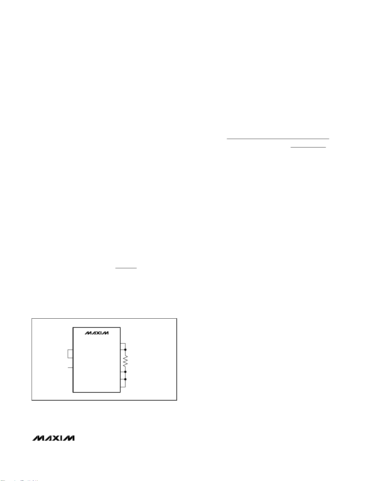
Detailed Description
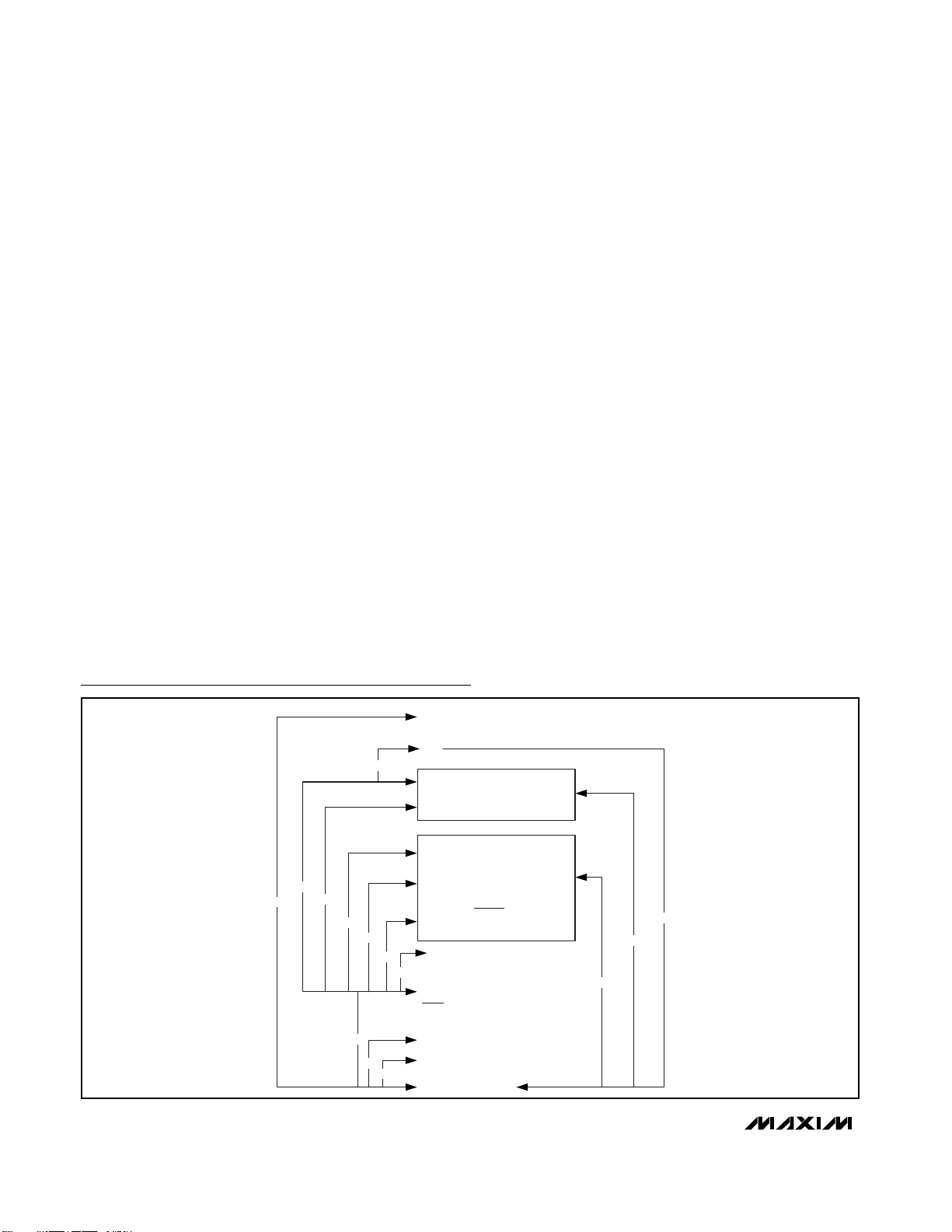
The MAX5042/MAX5043 PWM multimode power ICs
are designed for the primary side of voltage or currentmode isolated, forward or flyback power converters.
These devices provide a high degree of integration
aimed at reducing the cost and PC board area of isolated output power supplies. Use the MAX5042/MAX5043
primarily for 24V, 42V, or 48V power bus applications.
The MAX5042/MAX5043 provide a complete system
capable of delivering up to 50W of output power. The
MAX5042 contains a hot-swap controller in addition to
the PWM and power MOSFETs. The hot-swap section
requires an external MOSFET (QHS). Figure 1 details
the MAX5042 conceptual block diagram. CINrepresents
the input bulk storage capacitance of the PWM circuit
that requires the soft-start to reduce the inrush current
from the backplane. When input power is applied,
capacitor C
IN
is completely discharged and QHS is off.
An applied voltage higher than the default undervoltage
lockout threshold of the hot-swap controller (30.5V) for
more than 165ms (internal turn-on delay) causes the
gate voltage of QHS to start gradually increasing. This
results in a controlled slew-rate turn-on. The drain voltage of QHS falls at a rate of approximately 10V/ms,
drawing a current load from the backplane of approximately 1A for each 100µF of CINcapacitance. The
MAX5042’s PWM block is prevented from starting up
until the QHS MOSFET is fully enhanced. After QHS
completely turns on and the voltage across capacitor
CINis above the default startup voltage (31V) of the
PWM section, the hot swap enables the PWM block and
the soft-start cycle begins. Soft-start limits the amount of
current initially drawn from the primary during startup
and also prevents possible output-voltage overshoots.
The MAX5043, detailed in Figure 2, does not contain an
integrated hot-swap controller. The MAX5043 begins
operating when the input voltage exceeds both of the
undervoltage lockout voltages (at UVLO and DEN pins)
for 10ms.
The MAX5042/MAX5043 support both forward and flyback power topologies. In forward mode, the maximum
output power is approximately 50W. In flyback mode,
the maximum output power is approximately 20W. The
amount of power dissipated by the package limits the
output power. The MAX5042/MAX5043’s QFN package
features an exposed metal pad on the bottom of the
package. Solder the exposed pad directly to the most
negative supply in the system. Use a large copper area
to improve heat dissipation. Facilitate heat transfer with
thermal vias.
Two-Switch Power ICs with Integrated
Power MOSFETs and Hot-Swap Controller
12 ______________________________________________________________________________________
Pin Description (continued)
Figure 1. Simplified Diagram of a MAX5042-Based Isolated
Power Supply
PIN
MAX5042 MAX5043
47 25, 47 POSINPWM
48, 51, 54, 55 48, 51, 54, 55 DRNH
49, 50, 52, 53 49, 50, 52, 53 XFRMRH High-Side Connection for the Isolation Transformer
—27DEN
— 30 N.C. No Connection (MAX5043 Only). Leave unconnected.
NAME FUNCTION
PWM Analog Positive-Supply Input. Connect POSINPWM to the most positive input
supply rail.
Drain Connection of the Internal High-Side PWM Power MOSFET. Connect DRNH to
the most positive rail of the input supply.
Delayed Enable Input (MAX5043 Only). DEN is the center point of the delayed
enable divider. Use an external voltage-divider or a 100kΩ pullup resistor to the
most positive rail to override.
+V
POSINPWM
NEGIN
CIRCUIT
INTEGRATED
INTEGRATED
CONTROLLER
MAX5042
PWM
WITH
FETs
HOT-SWAP
BULK STORAGE CAPACITOR
QH
QL
QHS
(HOT-SWAPPED CAPACITOR)
C
IN
T1
PWMNEG, PWMPNEG
EXTERNAL
HOT-SWAP FET
L
V
OUT
C
OUT
Page 13

Set the switching frequency with a resistor and a
capacitor at RCOSC. Switching at 250kHz ensures
switching losses are minimal and external power passives are small enough for a compact circuit.
The MAX5042/MAX5043 incorporate an advanced set of
protection features that make them uniquely suitable
when high reliability and comprehensive fault protection
are required, as in telecommunication equipment powersupply applications. The MAX5042/MAX5043 15V linear
regulator output powers the 9V and 5V regulators used to
drive the gates and internal circuitry. A tertiary winding
connects to REG15 through a rectifier to power the
device after startup and reduces power dissipation in the
MAX5042/MAX5043 package. When REG15 is externally
powered, the internal 15V regulator is disabled.
Figures 3 and 4 show the block diagrams of the MAX5042
and MAX5043, respectively. The power-OK signals from
the hot-swap section, regulators, thermal shutdown, and
UVLO combine to generate the internal shutdown signal
SHDN. When asserted, SHDN disables the comparators
and oscillator. Deasserting SHDN releases the comparators and oscillators. The falling edge of SHDN is delayed
allowing the internal signals to settle before the PWM pulses appear. During the time between the falling edge of
SHDN and its delayed signal, the 10Ω internal MOSFET
(QB) from XFRMRH to PWMPNEG turns on, charging the
BST capacitor. After startup, this MOSFET also turns on
for approximately 300ns at each half period to help
charge the BST capacitor.
Power Topology
The two-switch forward-converter topology offers outstanding robustness against faults and transformer saturation while affording efficient use of the integrated
75mΩ power MOSFETs. Voltage-mode control with feedforward compensation allows the rejection of input supply disturbances within a single cycle similar to that of
current-mode controlled topologies. This control method
offers some significant benefits when compared with
current-mode control. These benefits include:
• No minimum duty-cycle requirement due to currentsignal filtering or blanking.
• Clean modulator ramp and higher amplitude for
increased stability.
• Stable bias point of the optocoupler LED and phototransistor for maximized control-loop bandwidth (in
current-mode applications, the optocoupler bias
point is output-load dependent).
• Predictable loop dynamics simplifying the design of
the control loop.
The two-switch power topology recovers energy stored
in both the magnetizing and parasitic leakage inductances of the transformer. Figure 7 shows the schematic diagram of a 48V input and 5V, 8A output isolated
power supply built with the MAX5042.
The MAX5042/MAX5043 also support current-mode control. Current-mode control has advantages such as a single-pole power circuit and a small-signal transfer
function that simplify the design of power supplies with
widely varying output capacitors.
Undervoltage Lockout
The MAX5042 has two UVLO functions. Both the hotswap section and the PWM section contain their own
undervoltage lockout comparators (HSEN and UVLO,
respectively). The MAX5043 lacks the hot-swapping
function, but retains the PWM UVLO and the deglitched
undervoltage lockout/power-on reset. In both cases,
internal resistors set a default input-voltage enable
threshold of 31V (typ).
The PWM default input voltage threshold value can be
adjusted by using an external divider in parallel with the
internal divider. The tolerances of the external divider
resistors dominate the precision of the UVLO trip point if
their values are smaller than those of the internal divider.
Override the default threshold by using:
MAX5042/MAX5043
Two-Switch Power ICs with Integrated
Power MOSFETs and Hot-Swap Controller
______________________________________________________________________________________ 13
Figure 2. Simplified Diagram of a MAX5043-Based Isolated
Power Supply
+V
POSINPWM
MAX5043
QH
PWM
CIRCUIT
WITH
INTEGRATED
FETs
QL
PWMNEG
BULK STORAGE CAPACITOR
C
IN
T1
L
V
OUT
C
OUT
R
=
He
VRRRRRVV
REF Hi Li Le Le Li IN REF
RRR VV
×××
Le Li Hi IN REF
×+
()
--
-
()
××
()
Page 14

MAX5042/MAX5043
Two-Switch Power ICs with Integrated
Power MOSFETs and Hot-Swap Controller
14 ______________________________________________________________________________________
Figure 3. Block Diagram of the MAX5042 Power IC
80µA
32µA
7.5V
MAX5042
REG5 OK
5V
IFLT
5V
UVLO
2.3V/1.6V
REG5
(5V)
OVRLD
CPWM
PWMNEG
RSQ
REG9 OK
REG15 OK
"1"
D
Q
R
7.5V
41
REG15
39
REG5
38
REG9
3
RCFF
11
FLTINT
4
RAMP
5
OPTO
6
CSS
35
PWMNEG
13
PWMSD
REG9
(9V)
PWMNEG
OVT
UVLO
REFOK
REG15OK
REG9OK
REG5OK
OVRLD
REG15 OK
CLK
REG5 OK
Q
T-FF
R
REG15
(15V)
RSQ
REF OK
SHDN
OSC
OVT
REF
(1.25V)
CUVLO
UVLO
LEADING-
RES
EDGE
DELAY
LEADING-
THERMAL
SHUTDOWN
+150°C
12°C HYSTERESIS
EDGE
DELAY
LEVEL
SHIFT
OVT
1.25V
1.125V
ONE
SHOT
7.5V
0.1Ω
QL
1.2MΩ
QH
0.1Ω
QB
10Ω
50kΩ
PWMNEG
47
POSINPWM
46
UVLO
37
PPWM
36
DRVDEL
7
BST
48
DRNH (51, 54, 55)
49
XFRMRH (50, 52, 53)
8
DRVIN
18
XFRMRL (19, 22, 23)
16
SRC (17, 20, 21, 24)
9
PWMPNEG
10
RCOSC
12
SYNC
CSOUT
POSINHS
HSEN
NEGIN (29)
ILIM
150mV
LEVEL SHIFT
TO PWM
460kΩ
GAIN = 10
IAMP
200mV
HOT-SWAP SECTION
40Ω
80V, DMOS
32
25
840kΩ
27
35kΩ
28
3V
HOT-SWAP
CONTROL
LOGIC
10MHz
33
CSP
34
CSN
31
HSDRAIN
30
HSGATE
26
HSOK
Page 15

MAX5042/MAX5043
Two-Switch Power ICs with Integrated
Power MOSFETs and Hot-Swap Controller
______________________________________________________________________________________ 15
Figure 4. Block Diagram of the MAX5043 Power IC
REG15
REG5
REG9
RCFF
FLTINT
RAMP
OPTO
PWMNEG (26)
PWMSD
CSS
80µA
32µA
7.5V
MAX5043
REG5 OK
5V
2.3V/1.6V
5V
UVLO
REG9 OK
REG5
(5V)
REG15 OK
7.5V
OVRLD
"1"
D
Q
R
IFLT
CPWM
50Ω
PWMNEG
RSQ
41
39
38
3
11
4
5
6
35
13
REG9
(9V)
PWMNEG
OVT
UVLO
REFOK
REG15OK
REG9OK
REG5OK
OVRLD
REG15 OK
CLK
REG5 OK
3Ω
Q
T-FF
R
REG15
(15V)
RSQ
REF OK
SHDN
OSC
OVT
REF
(1.25V)
UVLO
LEADING-
RES
EDGE
DELAY
THERMAL
SHUTDOWN
+150°C
12°C HYSTERESIS
CUVLO
LEADING-
EDGE
DELAY
LEVEL
SHIFT
1.25V
1.125V
OVT
ONE
SHOT
7.5V
QL
0.1Ω
1.2MΩ
QH
0.1Ω
QB
10Ω
50kΩ
PWMNEG
47
POSINPWM
46
UVLO
37
PPWM
36
DRVDEL
7
BST
48
DRNH (51, 54, 55)
49
XFRMRH (50, 52, 53)
8
DRVIN
18
XFRMRL (19, 22, 23)
16
SRC (17, 20, 21, 24)
9
PWMPNEG
10
RCOSC
12
SYNC
32
CSOUT
DEN
25
840kΩ
27
CDEN
35kΩ
28
1.25V
3V
1.125V
POSINPWM
PWMNEG (29, 31)
10ms
DELAY
GAIN = 10
IAMP
ILIM
200mV
150mV
10MHz
33
CSP
34
CSN
Page 16

MAX5042/MAX5043
where RHeis the external high-side resistor, RLeis the
external low-side resistor, R
Hi
is the internal high-side
resistor (1.2MΩ, typ), R
Le
is the internal low-side resistor
(50kΩ, typ), V
REF
is 1.27V (typ), and VINis the desired
threshold.
Use an external 100kΩ pullup resistor to POSINPWM to
override UVLO functionality for either lockout.
Internal Regulators
An internal high-voltage linear regulator provides a 15V
output at REG15. This serves as the input to the 9V regulator that provides bias for the internal MOSFET drivers. The 15V regulator also provides the bias for REG5,
a 5V supply used both by internal as well as external circuitry. Bypass the REG15, REG9, and REG5 regulators
with 1µF ceramic capacitors. A voltage greater than 18V
and less than 40V on REG15 disables the internal highvoltage startup regulator. The REG9 regulator steps
down the voltage on REG15 to an output of 9V with a
current limit of 100mA. The REG5 regulator steps down
the voltage on REG15 to an output of 5V with a current
limit of 40mA. Disabling the REG15 regulator by powering REG15 with an external power supply considerably
reduces the internal power dissipation in the
MAX5042/MAX5043. The voltage and power necessary
to override the REG15 internal regulator can be generated with a rectifier and an extra winding from the main
transformer.
Soft-Start
Program the MAX5042/MAX5043 soft-start with an
external capacitor between CSS and PWMNEG. When
the device turns on, the soft-start capacitor (C
CSS
)
charges with a constant current of 33µA, ramping up to
7.3V. During this time, OPTO is clamped to CSS + 0.6V.
This initially holds the duty cycle lower than the value
the regulator tries to impose, limiting the current inrush
and the voltage overshoot at the secondary. When the
MAX5042/MAX5043 turn off, the soft-start capacitor
internally discharges to PWMNEG.
Secondary-Side Synchronization
The MAX5042/MAX5043 provide convenient synchronization of the secondary-side synchronous rectifiers.
Figure 5 shows the connection diagram with a highspeed optocoupler. Choose an optocoupler with a
propagation delay of less than 50ns.
For optimum results, adjust the resistor connected to
DRVDEL to provide the required amount of delay
between the leading edge of the PPWM signal and the
turn-on of the power MOSFETs. Use the following formula to calculate the approximate resistance (R
DRVDEL
)
required to set the delay between the PPWM and the
power pulse applied to the transformer:
where t
DRVDEL
is the required delay from the rising edge
of PPWM to the switching of the internal power MOSFETs.
PWM Regulation
The MAX5042/MAX5043 are multimode PWM power
ICs supporting both voltage and current-mode control.
Voltage-Mode Control and the PWM Ramp
For voltage-mode control, the feed-forward PWM ramp
is generated at RCFF. From RCFF connect a capacitor
to PWMNEG and a resistor to POSINPWM. The ramp
generated is applied to the noninverting input of the
PWM comparator at RAMP and has a minimum voltage
of 1.5V to 2.5V. The slope of the ramp is determined by
the voltage at POSINPWM and affects the overall loop
gain. The ramp peak must remain below the dynamic
range of RCFF (0 to 5.5V). Assuming the maximum duty
cycle approaches 50% at a minimum input voltage
(PWM UVLO turn-on threshold), use the following formula to calculate the minimum value of either the ramp
capacitor or resistor:
where:
V
INUVLO
= the minimum input supply voltage (typically
the PWM UVLO turn-on voltage),
fs= the switching frequency,
V
r
P-P
= the peak-to-peak ramp voltage (2V, typ).
Two-Switch Power ICs with Integrated
Power MOSFETs and Hot-Swap Controller
16 ______________________________________________________________________________________
Figure 5. Secondary-Side Synchronous Rectifier Driver Using a
High-Speed Optocoupler
MAX5042/MAX5043
DRVDEL
PPWM
PWMNEG
R1
C1
0.22µF
Rt ns
DRVDEL DRVDEL
=−
()
RC
×≥
RCFF RCFF
R2
PS9715
OR EQUIVALENT
HIGH-SPEED
OPTOCOUPLER
100
()
⎛
⎜
⎝
V
INUVLO
×
2
fV
SrPP
-
5V
C2
k
Ω
⎞
⎟
⎠
ns
2
Page 17
Maximize the signal-to-noise ratio by setting the ramp
peak as high as possible. Calculate the low-frequency,
small-signal gain of the power stage (the gain from the
inverting input of the PWM comparator to the output)
using the following formula:
GPS= N
SP
✕ R
RCFF
✕ C
RCFF
✕ f
S
where NSP= the secondary to primary power transformer
turns ratio.
Current-Sense Amplifier and Current-Mode Control
The MAX5042/MAX5043 can also be programmed for
current-mode control (see Figure 6). This control
method offers beneficial advantages for certain applications. Current-mode control reduces the order of the
output filter, allowing easier control-loop compensation.
In current-mode control, the voltage across the currentsense resistor at SRC is amplified by the internal gainof-10 amplifier IAMP. The cycle-by-cycle current-limit
threshold is 156mV. This is the peak voltage amplified
by IAMP. A 200mV offset is added to this voltage. The
voltage at the output of the current-sense amplifier is:
V
CSOUT
= 2 + 10(V
CSP
- V
CSN
)
The low-frequency, small-signal gain of the power
stage (the gain from the inverting input of the PWM
comparator to the output) can be calculated using the
following formula:
where NPS= the primary to secondary power transformer turns ratio,
RL= the low-frequency output impedance,
R
SENSE
= the primary current-sense resistor value.
Oscillator and Synchronization
Program the MAX5042/MAX5043 oscillator using an RC
network at RCOSC with the resistor connected to REG5
and the capacitor connected to PWMNEG. The PWM
frequency is half the frequency at RCOSC.
Use the following formula to calculate the oscillator
components:
where C
PCB
= 14pF,
REG5 = 5V,
fS= switching frequency,
VTH= RCOSC peak trip level.
The delay programmed by the resistor at DRVDEL limits the power MOSFET’s maximum duty cycle to less
than 50 percent.
SYNC allows synchronization of the MAX5042/MAX5043
to an external clock. For proper synchronization, set the
external SYNC frequency 15% to 20% higher than the
programmed free-running frequency of the MAX5042/
MAX5043’s internal oscillator. The actual switching
frequency will be half the synchronizing frequency.
Integrating Fault Protection
The integrating fault protection feature allows the
MAX5042/MAX5043 to ignore transient overcurrent
conditions for a programmable amount of time, giving
the power supply time to behave like a current source
to the load. This can happen, for example, under loadcurrent transients when the control loop requests maximum current to keep the output voltage from going out
of regulation. Program the ignore time externally by
connecting a capacitor to FLTINT. Under sustained
overcurrent faults, the voltage across this capacitor
ramps up toward the FLTINT shutdown threshold (typically 2.7V). When FLTINT reaches the threshold, the
power supply shuts down. A high-value bleed resistor
connected in parallel with the FLTINT capacitor allows
the capacitor to discharge toward the restart threshold
(typically 1.8V). Crossing the restart threshold softstarts the supply again.
The ILIM comparator provides cycle-by-cycle current
limiting with a typical threshold of 156mV. The fault integration circuit works by forcing an 80µA current out of
FLTINT for one clock cycle every time the current-limit
comparator (Figures 3 and 4, ILIM) trips. Use the following formula to calculate the approximate capacitance (C
FLTINT
) needed for the desired shutdown time.
MAX5042/MAX5043
Two-Switch Power ICs with Integrated
Power MOSFETs and Hot-Swap Controller
______________________________________________________________________________________ 17
Figure 6. Simplified Connection Diagram for Current-Mode
Control
R
GN
=×
PS PS
R
SENSE
L
MAX5042/MAX5043
RAMP
CSOUT
OPTO
SRC
CSP
CSN
PWMPNEG
PWMNEG
RS
50mΩ
(APPROXIMATELY
35W TO 40W)
R
RCOSC
=
2
fC C
()
S RCOSC PCB
1
ln
+
⎛
V
REG
⎜
VV
⎝
REG TH
5
⎞
5
⎟
−
⎠
Page 18

MAX5042/MAX5043
where I
FLTINT
= 80µA,
tshis the desired ignore time during which current-limit
events from the current-limit comparator are ignored.
Some testing may be required to fine tune the actual
value of the capacitor.
Calculate the approximate bleed resistance (R
FLTINT
)
needed for the desired recovery time using the following formula:
where tRTis the desired recovery time.
Choose at least tRT= 10 x tSH. Typical values for t
SH
range from a few hundred microseconds to a few milliseconds.
Shutdown Modes
Latched Shutdown
The MAX5042/MAX5043 feature a latched shutdown that
terminates switching in the event of a serious fault.
External faults in synchronously rectified power supplies
cause a loss of control for the rectifiers. Either the body or
the external Schottky diodes conduct, resulting in a very
high power dissipation and a quick rise of the power-supply temperature. A thermal sensor placed on the same
ground plane as the secondary-side rectifiers can sense
this catastrophic increase in temperature and issue a
shutdown signal to PWMSD. Asserting PWMSD stops
switching and latches the fault until the power is cycled.
Connect PWMSD to REG5 to disable latched shutdown.
Functional Shutdown
Shut down the MAX5042/MAX5043 by pulling UVLO to
PWMNEG using an open-collector or open-drain transistor connected to PWMNEG. Pulling HSEN to NEGIN also
shuts down the MAX5042 after a 10ms turn-off delay.
Pulling DEN low also shuts down the MAX5043 with a
1ms turn-off delay. When HSEN is used, the MAX5042
goes through a full hot-swap startup sequence with a
165ms startup delay. The MAX5043 also has a 10ms
delay from when DEN asserts.
Thermal Shutdown
The MAX5042/MAX5043 feature internal thermal shutdown. Internal sensors monitor the high-power areas.
Thermal faults arise from excessive dissipation in the
power FETs or in the regulators. When the temperature
limit is reached, switching is terminated and the regulator
shuts down. The integration of thermal shutdown and the
power MOSFETs result in a very robust power circuit.
MAX5042 Hot-Swap Controller
The MAX5042 integrates a PWM power IC with a hotswap controller. The design allows a power supply built
around the MAX5042 to be safely hot-plugged into a
live backplane without causing a glitch on the powersupply rail. The hot-swap section operates from
POSINHS to NEGIN. The MAX5042 only requires an
external N-channel MOSFET to provide hot-swap control. Figures 1 and 3 detail hot-swap functionality.
The MAX5042 controls an external N-channel power
MOSFET placed in the negative power-supply pathway.
When power is applied, the MAX5042 keeps the MOSFET off. The MOSFET remains off indefinitely if HSEN is
below 1.26V, POSINHS is below the undervoltage lockout level (31V), or the die temperature exceeds
+150°C. If none of these conditions exist for 165ms, the
MAX5042 gradually turns on the MOSFET, allowing the
voltage on HSDRAIN to fall no faster than 10V/ms.
During this period, the PWM block remains in shutdown. The inrush current through the external MOSFET
(and therefore through the capacitor C
IN
) is limited to a
level proportional to its capacitance, and the constant
HSDRAIN slew rate. After the MOSFET completely turns
on, and HSDRAIN falls to its final value, the hot-swap
period is terminated and the PWM section of the IC
powers up.
HSEN offers external control of the MAX5042, facilitating power-supply sequencing. HSEN can also be used
to change the undervoltage lockout level using an
external divider network, if necessary. Undervoltage
lockout keeps the external hot-swap MOSFET switched
off as long as the magnitude of the input voltage is
below the desired level. There is a 10ms turn-off delay
on the HSEN signal.
A power-good output, HSOK, asserts when the external
MOSFET completely turns on. HSOK is an open-drain
output referenced to NEGIN, and can withstand up to
80V above NEGIN.
Two-Switch Power ICs with Integrated
Power MOSFETs and Hot-Swap Controller
18 ______________________________________________________________________________________
C
FLTINT
R
FLTINT
It
≅
≅
C
FLTINT
×
FLTINT SH
.
14
t
RT
23
⎛
ln
⎜
⎝
16
.
⎞
⎟
⎠
.
Page 19
Determining Hot-Swap Inrush Current
Calculate the hot-swap inrush current using the following formula:
where:
CIN= the load capacitance,
S
HSLR
is the MAX5042 hot-swap slew rate magnitude
given in the Electrical Characteristics table.
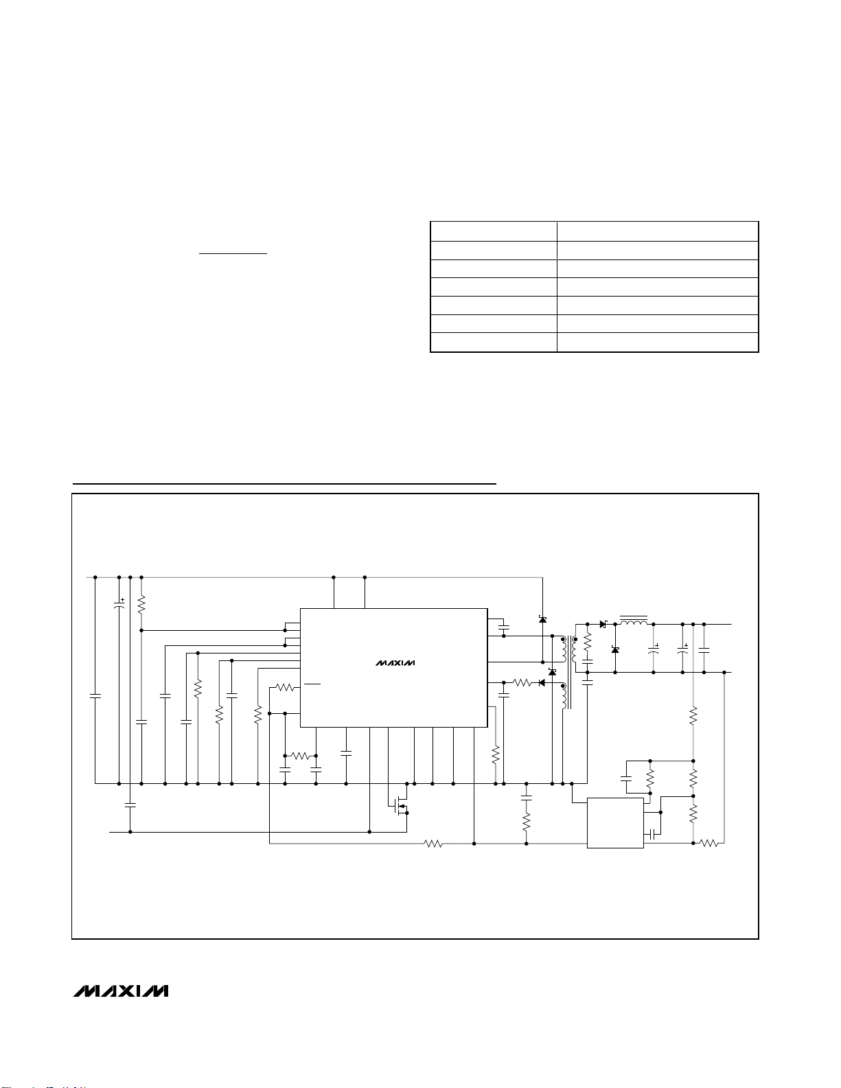
For example, assuming an input bulk capacitance of
100µF, and using the typical value of 10V/ms for the
slew rate, the calculated inrush current is 1A. See Table
1 for suggested external hot-swap MOSFETs.
MAX5042/MAX5043
Two-Switch Power ICs with Integrated
Power MOSFETs and Hot-Swap Controller
______________________________________________________________________________________ 19
Table 1. MAX5042 Suggested External
Hot-Swap MOSFETs
Figure 7. MAX5042 Typical Application Circuit (48V Power Supply with Hot-Swap Capability)
Typical Application Circuits
dV
IC
==
CIN
IN
HSDRAIN
dt
CS
IN HSLR
V
IN+
32V TO 72V
MAXIMUM I
(A) SUGGESTED EXTERNAL MOSFET
LOAD
0.25 IRFL110
0.5 IRFL4310
1 IRFR3910
2 IRF540NS
3 IRF1310NS
4 IRF1310NS
220µF
100V
C1
C30
0.68µF
100V
NEGIN
C20
0.1µF
100V
R12
200kΩ
1%
C9
220pF
0.1µF
POSINPWM
HSEN
C14
100pF
DRNH UVLO
NEGIN HSGATE HSDRAIN
CSS
C11
0.1µF
U1
MAX5042
PWMNEG,
CSN
N1
(HOT-SWAP MOSFET)
R21
1.24kΩ
1%
RAMP
RCFF
REG9
DRVIN
FLTINT
DRVDEL
SYNC
R22
C25
0.22µF
10kΩ
10kΩ
PWMSD
R20
R15
24.9kΩ
1%
C13
1µF
REG5
RCOSC
R13
1MΩ
C3
1µF
R14
C12
10kΩ
XFRMRH
XFRMRL
CSP, SRC
PWMPNEG OPTO
REG15
BST
33mΩ
C6
0.1µF
R9
15Ω
C7
1µF
R10
1%
C8
0.33µF
R6
200Ω
1%
L1
4.4µH
D1
D2
D4
D3
T1
R11
E
C
20Ω
1%
C16
0.001µF
C5
0.0047µF
0.15µF
FOD2712
C17
C18
150µF
150µF
6.3V
6.3V
R4
10Ω
COMP
R3
150Ω
1%
LED
FB
C15
0.1µF
GND
C19
U2
R1
25.5kΩ
1%
R2
8.25kΩ
1%
10Ω
5V
8A
C4
0.1µF
SGND
R5
1%
Page 20
MAX5042/MAX5043
Two-Switch Power ICs with Integrated
Power MOSFETs and Hot-Swap Controller
20 ______________________________________________________________________________________
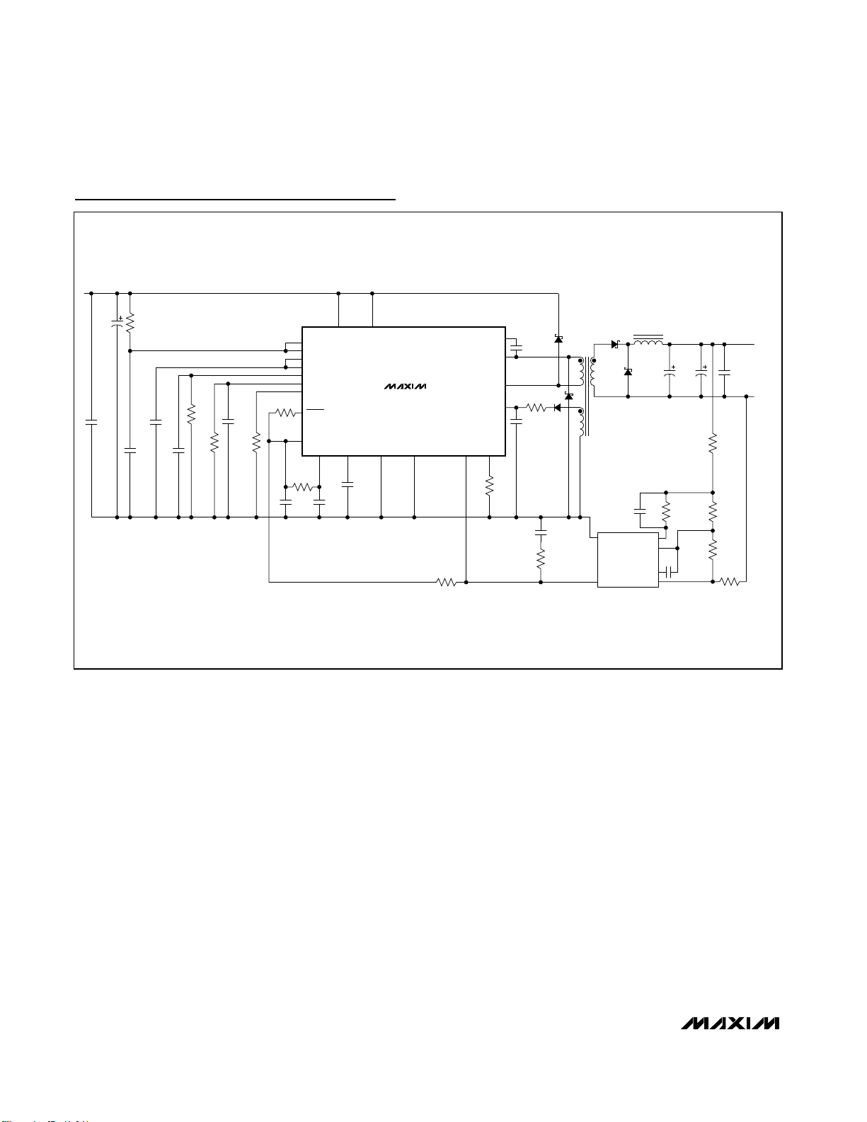
Figure 8. MAX5043 Typical Application Circuit (48V Power Supply without Hot-Swap Capability, this Circuit has not been Tested)
Typical Application Circuits (continued)
V
IN+
32V TO 72V
C1
100V
0.68µF
100V
R12
200kΩ
1%
C9
220pF
0.1µF
POSINPWM DRNH UVLO
RAMP
RCFF
REG9
DRVIN
FLTINT
DRVDEL
SYNC
R22
10kΩ
10kΩ
PWMSD
R20
R15
24.9kΩ
1%
C13
1µF
REG5
RCOSC
C14
100pF
CSS
C11
0.1µF
R13
C25
1MΩ
C13
1µF
C12
10kΩ
0.22µF
R14
PWMNEG
U1
MAX5043
PWMNEG,
CSN
R21
1.24kΩ
1%
OPTO
33mΩ
SRC, CSP
R10
1%
XFRMRH
XFRMRL
REG15
BST
C6
0.1µF
C7
1µF
D1
R9
15Ω
D4
C8
0.33µF
R6
200Ω
1%
D3
T1
D2
0.15µF
E
C
220µF
PWMNEG
C19
U2
FOD2712
4.4µH
COMP
GND
L1
150µF
LED
5V
10A
C17
C18
150µF
6.3V
6.3V
R3
150Ω
1%
FB
C15
0.1µF
C4
0.1µF
SGND
R4
10Ω
R1
25.5kΩ
1%
R2
8.25kΩ
1%
R5
10Ω
1%
Page 21
MAX5042/MAX5043
Two-Switch Power ICs with Integrated
Power MOSFETs and Hot-Swap Controller
______________________________________________________________________________________ 21
Chip Information
TRANSISTOR COUNT: 35,247
PROCESS: BiCMOS DMOS
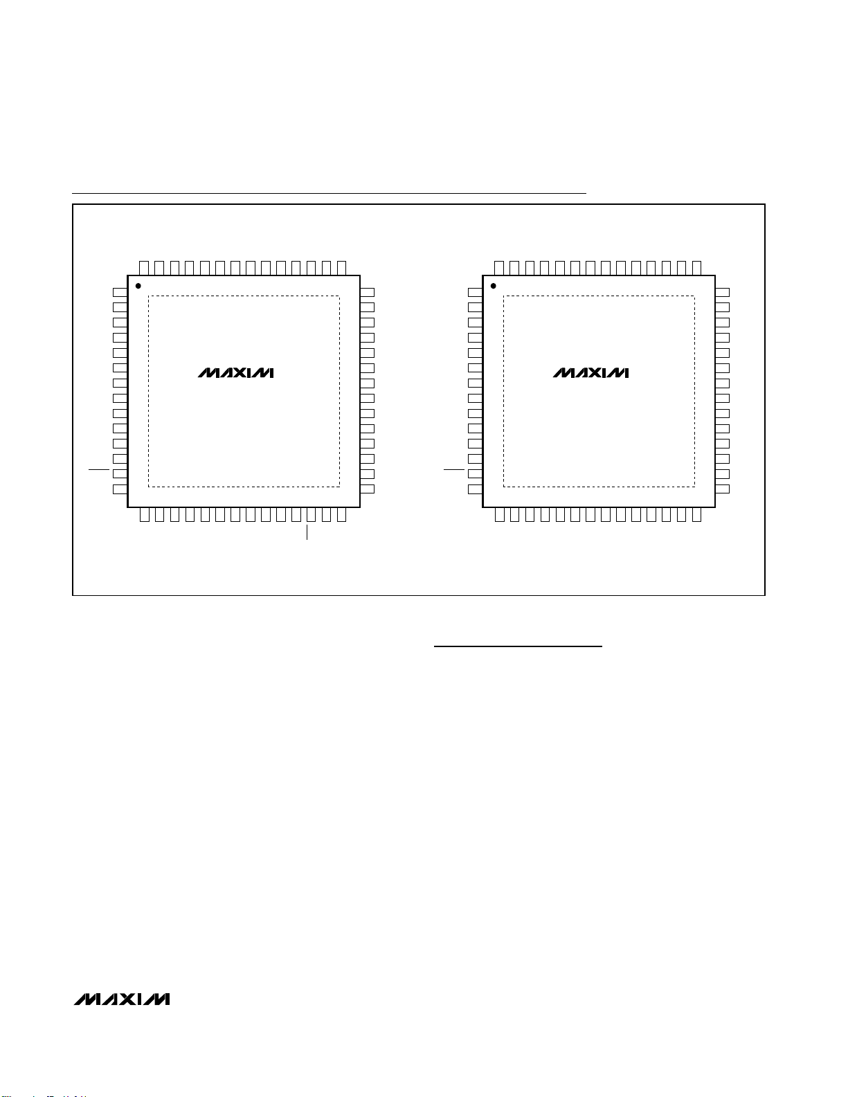
Pin Configurations
TOP VIEW
17
XFRMRH51DRNH
52
MAX5042ATN
19
XFRMRL18XFRMRL
THIN QFN
21
SRC20SRC
23
24
XFRMRL22XFRMRL
SRC
25
POSINHS
26
HSOK
N.C.
43
42 N.C.
41 REG15
40 N.C.
39 REG5
38 REG9
37 PPWM
36 DRVDEL
35 PWMNEG
34 CSN
33 CSP
32 CSOUT
31 HSDRAIN
30 HSGATE
NEGIN
29
28
27
HSEN
NEGIN
N.C. 1
N.C.
RCFF
RAMP 4
OPTO 5
CSS 6
BST 7
DRVIN 8
PWMPNEG 9
RCOSC 10
FLTINT 11
SYNC 12
PWMSD 13
N.C. 14
N.C.55DRNH54DRNH53XFRMRH50XFRMRH49XFRMRH48DRNH47POSINPWM46UVLO45N.C.44N.C.
56
2
3
15
17
N.C.
SRC16SRC
N.C.55DRNH54DRNH53XFRMRH50XFRMRH49XFRMRH48DRNH47POSINPWM46UVLO45N.C.44N.C.
56
N.C. 1
2
N.C.
RCFF
3
RAMP 4
OPTO 5
CSS 6
BST 7
DRVIN 8
PWMPNEG 9
RCOSC 10
FLTINT 11
SYNC 12
PWMSD 13
N.C. 14
15
N.C.
SRC16SRC
EXPOSED PADDLE CONNECTED TO NEGIN. EXPOSED PADDLE CONNECTED TO PWMNEG.
XFRMRH51DRNH
52
MAX5043ETN
19
XFRMRL18XFRMRL
THIN QFN
N.C.
43
42 N.C.
41 REG15
40 N.C.
39 REG5
38 REG9
37 PPWM
36 DRVDEL
35 PWMNEG
34 CSN
33 CSP
32 CSOUT
31 PWMNEG
30 N.C.
29
21
23
25
SRC20SRC
24
SRC
XFRMRL22XFRMRL
27
DEN
PWMNEG26PWMNEG
POSINPWM
28
PWMNEG
Page 22
MAX5042/MAX5043
Two-Switch Power ICs with Integrated
Power MOSFETs and Hot-Swap Controller
Maxim cannot assume responsibility for use of any circuitry other than circuitry entirely embodied in a Maxim product. No circuit patent licenses are
implied. Maxim reserves the right to change the circuitry and specifications without notice at any time.
22 ____________________Maxim Integrated Products, 120 San Gabriel Drive, Sunnyvale, CA 94086 408-737-7600
© 2004 Maxim Integrated Products Printed USA is a registered trademark of Maxim Integrated Products.
Package Information
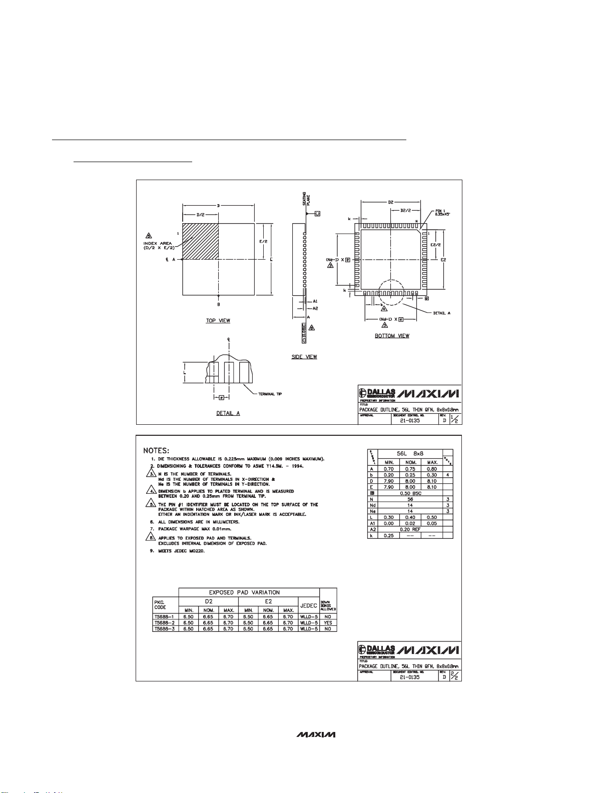
(The package drawing(s) in this data sheet may not reflect the most current specifications. For the latest package outline information,
go to www.maxim-ic.com/packages
.)
56L THIN QFN.EPS
 Loading...