_______________General Description
The MAX503 is a low-power, 10-bit, voltage-output digitalto-analog converter (DAC) that uses single 5V or dual ±5V
supplies. This device has an internal voltage reference plus
an output buffer amplifier. Operating current is only 250µA
from a single 5V supply, making it ideal for portable and
battery-powered applications. In addition, the shrink smalloutline package (SSOP) measures only 0.1 square inches,
using less board area than an 8-pin DIP. 10-bit resolution is
achieved through laser trimming of the DAC, op amp, and
reference. No further adjustments are necessary.
Internal gain-setting resistors can be used to define a DAC
output voltage range of 0V to +2.048V, 0V to +4.096V, or
±2.048V. Four-quadrant multiplication is possible without
the use of external resistors or op amps. The parallel logic
inputs are double buffered and are compatible with 4-bit, 8bit, and 16-bit microprocessors. For a hardware and software compatible 12-bit upgrade, refer to the MAX530 data
sheet. For DACs with similar features but with a serial data
interface, refer to the MAX504/MAX515 data sheet.
________________________Applications
Battery-Powered Data-Conversion Products
Minimum Component-Count Analog Systems
Digital Offset/Gain Adjustment
Industrial Process Control
Arbitrary Function Generators
Automatic Test Equipment
Microprocessor-Controlled Calibration
____________________________Features
♦ Buffered Voltage Output
♦ Internal 2.048V Voltage Reference
♦ Operates from Single 5V or Dual ±5V Supplies
♦ Low Power Consumption:
250µA Operating Current
40µA Shutdown-Mode Current
♦ SSOP Package Saves Space
♦ Relative Accuracy: ±
1
/
2
LSB Max Over
Temperature
♦ Guaranteed Monotonic Over Temperature
♦ 4-Quadrant Multiplication with No External
Components
♦ Power-On Reset
♦ Double-Buffered Parallel Logic Inputs
______________Ordering Information
MAX503
5V, Low-Power, Parallel-Input,
Voltage-Output, 10-Bit DAC
________________________________________________________________
Maxim Integrated Products
1
24
23
22
21
20
19
18
17
1
2
3
4
5
6
7
8
D6/S0
V
DD
ROFS
RFB
D2
D9/D1
D8/D0
D7/S1
TOP VIEW
VOUT
V
SS
REFOUT
REFGND
A0
D5
D4
D3
16
15
14
13
9
10
11
12
LDAC
CLR
AGND
REFIN
DGND
CS
WR
A1
DIP/SO/SSOP
MAX503
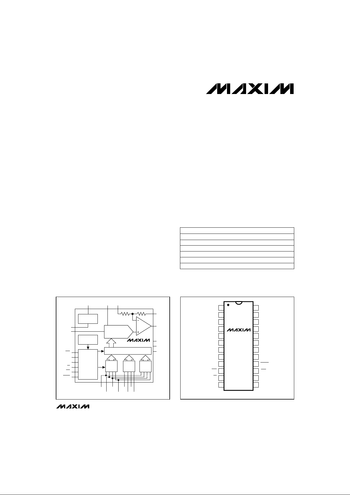
__________________Pin Configuration
MAX503
REFOUT REFIN ROFS
2.048V
REFERENCE
POWER-ON
RESET
DAC
CONTROL
LOGIC
REFGND
AGND
CLR
A0
A1
CS
WR
LDAC
V
DD
DGND
V
SS
VOUT
RFB
17
14
DAC LATCH
NBL
INPUT
LATCH
D6/S0
D7/S1
D8/D0
D2
D9/D1
D4
D3
D5
NBM
INPUT
LATCH
NBH
INPUT
LATCH
24 1
234567
21
20
23
12
19
18 13 22
15
8
9
11
10
16
10-BIT DAC LATCH
________________Functional Diagram
Call toll free 1-800-998-8800 for free samples or literature.
PART TEMP. RANGE PIN-PACKAGE
MAX503CNG 0°C to +70°C 24 Narrow Plastic DIP
MAX503CWG 0°C to +70°C 24 Wide SO
MAX503CAG 0°C to +70°C 24 SSOP
19-0279; Rev 0; 8/94
Refer to the MAX530 for military temperature or die equivalents.
MAX503ENG -40°C to +85°C 24 Narrow Plastic DIP
MAX503EWG -40°C to +85°C 24 Wide SO
MAX503EAG -40°C to +85°C 24 SSOP
MAX503
5V, Low-Power, Parallel-Input,
Voltage-Output, 10-Bit DAC
2 _______________________________________________________________________________________
ABSOLUTE MAXIMUM RATINGS
VDDto DGND and VDDto AGND................................-0.3V, +6V
V
SS
to DGND and VSSto AGND .................................-6V, +0.3V
V
DD
to VSS............................................................... -0.3V, +12V
AGND to DGND........................................................-0.3V, +0.3V
REFGND to AGND.........................................-0.3V, (V
DD
+ 0.3V)
Digital Input Voltage to DGND .................... -0.3V, (V
DD
+ 0.3V)
REFIN..................................................(V
SS
- 0.3V), (VDD+ 0.3V)
REFOUT..............................................(V
SS
- 0.3V), (VDD+ 0.3V)
REFOUT to REFGND.................................... -0.3V, (V
DD
+ 0.3V)
RFB ....................................................(V
SS
- 0.3V), (VDD+ 0.3V)
ROFS ..................................................(V
SS
- 0.3V), (VDD+ 0.3V)
VOUT to AGND (Note 1) .............................................. V
SS,VDD
Continuous Current, Any Input ........................................±20mA
Continuous Power Dissipation (T
A
= +70°C)
Narrow Plastic DIP (derate 13.33mW/°C above +70°C)...1067mW
Wide SO (derate 11.76mW/°C above +70°C)............... 941mW
SSOP (derate 8.00mW/°C above +70°C) ......................640mW
Operating Temperature Ranges
MAX503C_G .........................................................0°C to +70°C
MAX503E_G ......................................................-40°C to +85°C
Storage Temperature Range.............................-65°C to +165°C
Lead Temperature (soldering, 10sec) ........................... +300°C
Stresses beyond those listed under “Absolute Maximum Ratings” may cause permanent damage to the device. These are stress ratings only, and functional
operation of the device at these or any other conditions beyond those indicated in the operational sections of the specifications is not implied. Exposure to
absolute maximum rating conditions for extended periods may affect device reliability.
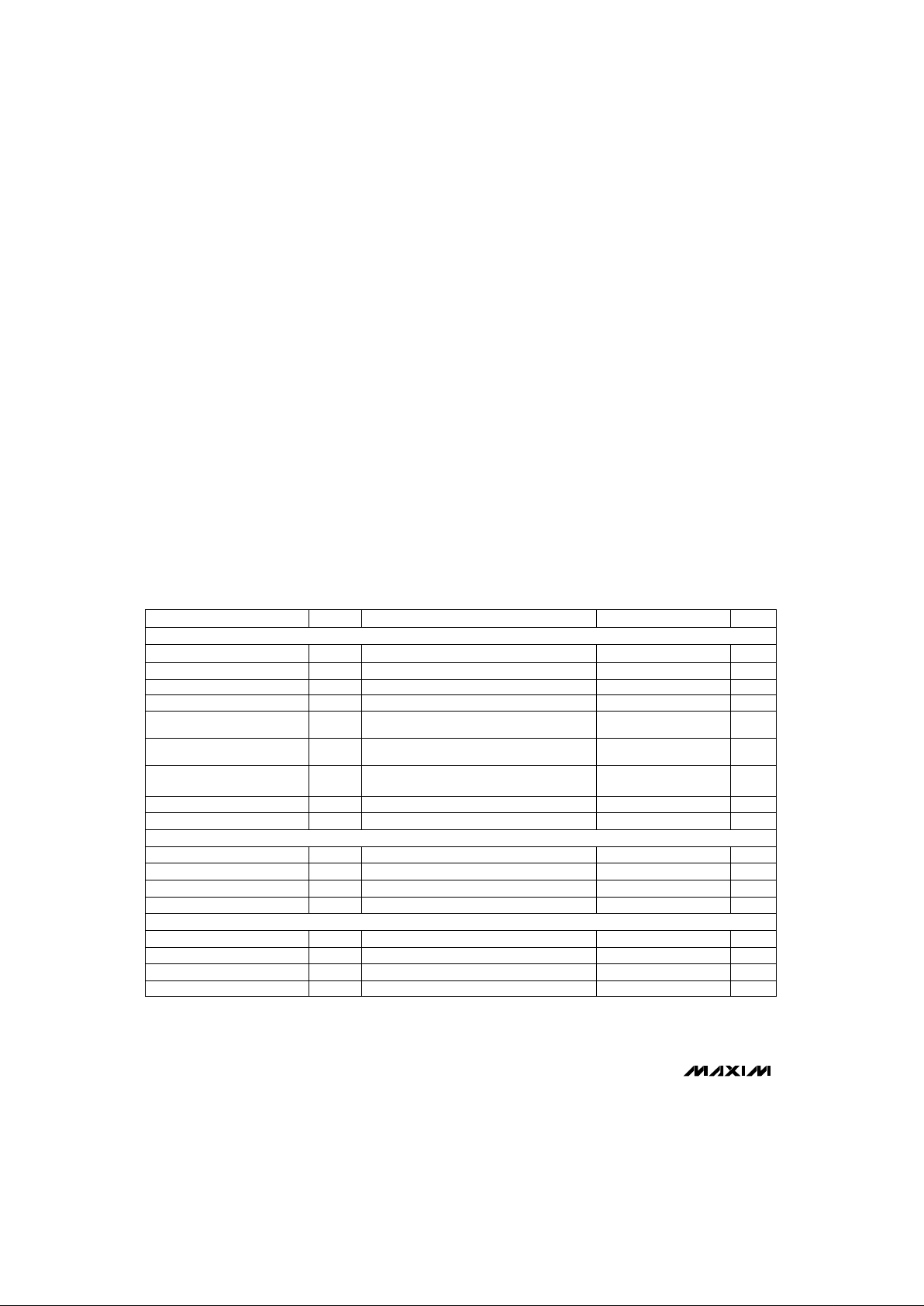
PARAMETER SYMBOL MIN TYP MAX UNITS
Differential Nonlinearity DNL ±1 LSB
Unipolar Offset Error V
OS
0 0.25 3 LSB
Unipolar Offset
Temperature Coefficient
TCV
OS
3 ppm/°C
Unipolar Offset-Error
Supply Rejection
PSRR 0.1 LSB/V
Resolution
STATIC PERFORMANCE
N 10 Bits
Gain-Error Temperature Coefficient 1 ppm/°C
Gain-Error Power-Supply Rejection PSRR 0.1 LSB/V
DAC VOLTAGE OUTPUT (VOUT)
Output Voltage Range 0V
DD
- 0.4 V
Resistive Load 2 kΩ
DC Output Impedance 0.2 Ω
Short-Circuit Current I
SC
12 mA
REFERENCE INPUT (REFIN)
Reference Input Range 0V
DD
- 2 V
Reference Input Resistance 40 kΩ
Reference Input Capacitance 10 50 pF
AC Feedthrough -80 dB
CONDITIONS
Guaranteed monotonic
4.5V ≤ VDD≤ 5.5V
4.5V ≤ VDD≤ 5.5V
VOUT = 2V, load regulation ≤ ±0.5LSB
Code dependent, minimum at code 0101...
Code dependent (Note 3)
(Note 4)
Gain Error (Note 2) GE LSB±1
Note 1: The output may be shorted to VDD, VSS, DGND, or AGND if the continuous package power dissipation and current ratings
are not exceeded. Typical short-circuit currents are 20mA.
ELECTRICAL CHARACTERISTICS—Single +5V Supply
(VDD= 5V, VSS= 0V, AGND = DGND = REFGND = 0V, REFIN = 2.048V (external), RFB = ROFS = VOUT, C
REFOUT
= 33µF,
RL= 10kΩ, CL= 100pF, TA= T
MIN
to T
MAX
, unless otherwise noted.)
DAC latch = all 1s,
VOUT < VDD- 0.4V (Note 2)
Relative Accuracy INL ±0.5 LSB(Note 2)
MAX503
5V, Low-Power, Parallel-Input,
Voltage-Output, 10-Bit DAC
_______________________________________________________________________________________ 3
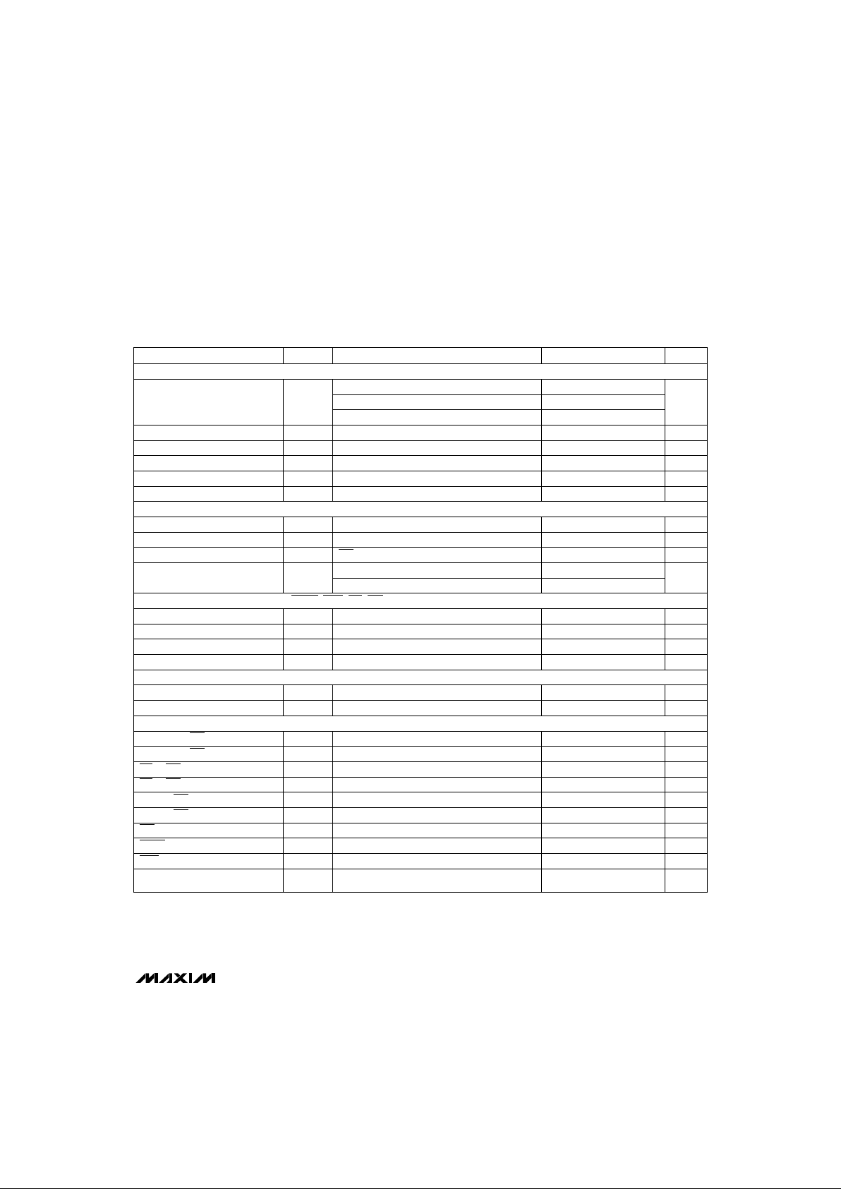
ELECTRICAL CHARACTERISTICS—Single +5V Supply (continued)
(VDD= 5V, VSS= 0V, AGND = DGND = REFGND = 0V, REFIN = 2.048V (external), RFB = ROFS = VOUT, C
REFOUT
= 33µF,
R
L
= 10kΩ, CL= 100pF, TA= T
MIN
to T
MAX
, unless otherwise noted.)
PARAMETER
Temperature Coefficient
SYMBOL MIN TYP MAX UNITS
Reference Tolerance V
REFOUT
ppm/°C
2.011 2.085
DYNAMIC PERFORMANCE
V2.015 2.081
REFERENCE OUTPUT (REFOUT)
Voltage Output Slew Rate
Reference Output Resistance R
REFOUT
2 Ω
Power-Supply Rejection Ratio PSRR 200 µV/V
0.15 0.25 V/µs
Voltage Output Settling Time
Noise Voltage e
n
400
25
µVp-p
µs
30
Digital Feedthrough 5 nV-s
68
Signal-to-Noise Plus
Distortion Ratio
SINAD
68
dB
DIGITAL INPUTS (S0, S1, D0–D9, LDAC, CLR, CS, WR, A0, A1)
Logic High Input V
IH
2.4 V
Logic Low Input V
IL
0.8 V
Digital Leakage Current ±1 µA
Digital Input Capacitance 8 pF
POWER SUPPLIES
CONDITIONS
(Note 5)
4.5V ≤ VDD≤ 5.5V
TA= +25°C
To ±0.5LSB, VOUT = 2V
WR = VDD, digital inputs all 1s to all 0s
Unity gain (Note 4)
Gain = 2 (Note 4)
VIN= 0V or V
DD
2.024 2.048 2.072TA= +25°C
0.1Hz to 10kHz
Positive Supply-Voltage Range V
DD
4.5 5.5 V
Positive Supply Current I
DD
Outputs unloaded, all digital inputs = 0V or V
DD
250 400 µA
SWITCHING CHARACTERISTICS
Address to WR Setup t
AWS
5 ns
Address to WR Hold t
AWH
5 ns
CS to WR Setup t
CWS
0 ns
CS to WR Hold t
CWH
0 ns
Data to WR Setup
t
DS
45 ns
Data to WR Hold
t
DH
0 ns
WR Pulse Width t
WR
45 ns
LDAC Pulse Width t
LDAC
45 ns
CLR Pulse Width t
CLR
45 ns
Internal Power-On Reset
Pulse Width
t
POR
(Note 3) 1.3 10 µs
Required External Capacitor C
REFOUT
3.3 µF
MAX503E
MAX503C
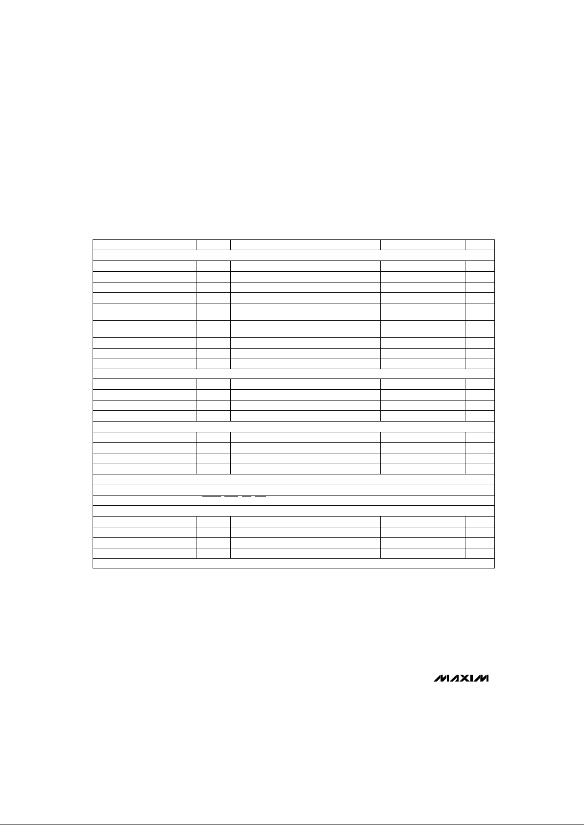
ELECTRICAL CHARACTERISTICS—Dual ±5V Supplies
(VDD= 5V, VSS= -5V, AGND = DGND = REFGND = 0V, REFIN = 2.048V (external), RFB = ROFS = VOUT, C
REFOUT
= 33µF,
R
L
= 10kΩ, CL= 100pF, TA= T
MIN
to T
MAX
, unless otherwise noted.)
Note 2: In single supply, INL and GE are calculated from code 3 to code 1023 (code excludes S0 and S1).
Note 3: Guaranteed by design.
Note 4: REFIN = 1kHz, 2.0Vp-p.
Note 5: Tested at I
OUT
= 100µA. The reference can typically source up to 5mA (see
Typical Operating Characteristics
).
MAX503
5V, Low-Power, Parallel-Input,
Voltage-Output, 10-Bit DAC
4 _______________________________________________________________________________________
SWITCHING CHARACTERISTICS—Specifications are identical to those under Single +5V Supply
POWER SUPPLIES
Positive Supply Voltage V
DD
4.5 5.5 V
Negative Supply Voltage V
SS
-5.5 0 V
Positive Supply Current I
DD
Outputs unloaded, all digital inputs = 0V or V
DD
250 400 µA
Negative Supply Current I
SS
Outputs unloaded, all digital inputs = 0V or V
DD
150 200 µA
PARAMETER
DAC VOLTAGE OUTPUT (VOUT)
SYMBOL MIN TYP MAX
DYNAMIC PERFORMANCE—Specifications are identical to those under Single +5V Supply
DIGITAL INPUTS (S0, S1, D0–D9, LDAC, CLR, CS, WR, A0, A1)—Specifications are identical to those under Single +5V Supply
UNITS
Bipolar Offset Error V
OS
±3
Output Voltage Range
LSB
Differential Nonlinearity
VSS+ 0.4 VDD- 0.4
DNL ±1 LSB
V
Resolution N
Bipolar Offset-Error
Power-Supply Rejection
Resistive Load
Bipolar Offset
Temperature Coefficient
TCV
OS
3 ppm/°C
2 kΩ
DC Output Impedance
Gain-Error Temperature Coefficient TC 1
0.2
ppm/°C
Gain-Error Power-Supply Rejection
Ω
PSRR 0.1 LSB/V
Short-Circuit Current I
SC
20 mA
REFERENCE INPUT (REFIN)
10
REFERENCE OUTPUT (REFOUT)—Specifications are identical to those under Single +5V Supply
Reference Input Range
STATIC PERFORMANCE
VSS+ 2 V
DD
- 2 V
Reference Input Resistance 40 kΩ
Reference Input Capacitance
Bits
PSRR
10 50 pF
AC Feedthrough -80 dB
0.1 LSB/V
CONDITIONS
Guaranteed monotonic
4.5V ≤ VDD≤ 5.5V, -5.5V ≤ V
SS
≤ -4.5V
VOUT = 2V, load regulation ≤ ±0.5LSB
4.5V ≤ VDD≤ 5.5V, -5.5V ≤ VSS≤ -4.5V
Code dependent, minimum at code 0101...
Code dependent (Note 3)
(Note 4)
Gain Error ±1 LSB
Relative Accuracy INL +0.5 LSB
MAX503
5V, Low-Power, Parallel-Input,
Voltage-Output, 10-Bit DAC
_______________________________________________________________________________________
5
12
0
0 0.8
OUTPUT SINK CAPABILITY vs.
OUTPUT PULL-DOWN VOLTAGE
2
10
MAX503-1
OUTPUT PULL-DOWN VOLTAGE (V)
OUTPUT SINK CAPABILITY (mA)
0.6
6
4
0.2 0.4
8
1.0
14
16
6
0
04
OUTPUT SOURCE CAPABILITY vs.
OUTPUT PULL-UP VOLTAGE
1
5
MAX503-2
OUTPUT PULL-UP VOLTAGE (V)
OUTPUT SOURCE CAPABILITY (mA)
3
3
2
12
4
5
7
8
300
230
-60 -20 60 140
SUPPLY CURRENT vs. TEMPERATURE
250
280
TEMPERATURE (°C)
SUPPLY CURRENT (µA)
20 100
260
290
270
240
-40 0 40 80 120
MAX503-5
4
-14
1 100 100k
GAIN vs. FREQUENCY
-12
MAX503-6
FREQUENCY (Hz)
GAIN (dB)
-8
-4
0
2
-2
-6
-10
1k 10k
REFIN = 4Vp-p
DUAL SUPPLIES (±5V)
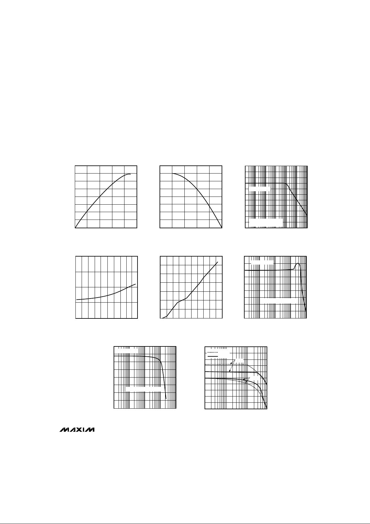
__________________________________________Typical Operating Characteristics
(Single +5V supply, unity gain, code = all 1s, TA = +25°C, unless otherwise noted.)
-110
0
1 10 1k 100k
ANALOG FEEDTHROUGH vs.
FREQUENCY
-30
-70
MAX503-3
FREQUENCY (Hz)
ANALOG FEEDTHROUGH (dB)
100 10k 1M
-100
-90
-80
-60
-50
-40
-20
-10
REFIN = 2V
p-p
CODE = ALL 0s,
DUAL SUPPLIES (±5V)
2.055
2.045
-60 120
REFERENCE VOLTAGE vs.
TEMPERATURE
MAX503-4
TEMPERATURE (°C)
REFERENCE VOLTAGE (V)
60
2.050
-20 20 80
100400-40
140
80
0
10 1k 100k
AMPLIFIER SIGNAL-TO-NOISE RATIO
10
MAX503-7
FREQUENCY (Hz)
SIGNAL-TO-NOISE RATIO (dB)
20
40
60
30
50
70
10k100
REFIN = 4Vp-p
DUAL SUPPLIES (±5V)
200
-300
1
GAIN AND PHASE vs.
FREQUENCY
-100
100
FREQUENCY (kHz)
GAIN (dB)
10 100
0
-200
800
-180
0
180
GAIN
PHASE
(G = 2)
(G = 1)
PHASE SHIFT (Degrees)
MAX503-8
 Loading...