

Page 1
现货库存、技术资料、百科信息、热点资讯,精彩尽在鼎好!
General Description
The MAX5038A/MAX5041A dual-phase, PWM controllers
provide high-output-current capability in a compact
package with a minimum number of external components. The MAX5038A/MAX5041A utilize a dual-phase,
average-current-mode control that enables optimal use
of low R
DS(ON)
MOSFETs, eliminating the need for exter-
nal heatsinks even when delivering high output currents.
Differential sensing enables accurate control of the output voltage, while adaptive voltage positioning provides
optimum transient response. An internal regulator
enables operation with input voltage ranges of +4.75V to
+5.5V or +8V to +28V. The high switching frequency, up
to 500kHz per phase, and dual-phase operation allow
the use of low-output inductor values and input capacitor
values. This accommodates the use of PC boardembedded planar magnetics achieving superior reliability, current sharing, thermal management, compact size,
and low system cost.
The MAX5038A/MAX5041A also feature a clock input
(CLKIN) for synchronization to an external clock, and a
clock output (CLKOUT) with programmable phase delay
(relative to CLKIN) for paralleling multiple phases. The
MAX5038A/MAX5041A also limit the reverse current in
case the bus voltage becomes higher than the regulated output voltage. The MAX5038A offers a variety of factory-trimmed preset output voltages (see Selector Guide)
and the MAX5041A offers an adjustable output voltage
between +1.0V to +3.3V.
The MAX5038A/MAX5041A operate over the extended
temperature range (-40°C to +85°C) and are available
in a 28-pin SSOP package. Refer to the MAX5037A and
MAX5065/MAX5067 data sheets for a VRM 9.0/VRM 9.1compatible, VID-controlled, adjustable output voltage
controller in a 44-pin MQFP/thin QFN or 28-pin SSOP
package.
Applications
Servers and Workstations
Point-of-Load High-Current/High-Density
Telecom DC-DC Regulators
Networking Systems
Large-Memory Arrays
RAID Systems
High-End Desktop Computers
Features
♦ +4.75V to +5.5V or +8V to +28V Input Voltage
Range
♦ Up to 60A Output Current
♦ Internal Voltage Regulator for a +12V or +24V
Power Bus
♦ True Differential Remote Output Sensing
♦ Two Out-Of-Phase Controllers Reduce Input
Capacitance Requirement and Distribute Power
Dissipation
♦ Average-Current-Mode Control
Superior Current Sharing Between Individual
Phases and Paralleled Modules
Accurate Current Limit Eliminates MOSFET and
Inductor Derating
♦ Limits Reverse-Current Sinking in Paralleled
Modules
♦ Integrated 4A Gate Drivers
♦ Selectable Fixed Frequency 250kHz or 500kHz per
Phase (Up to 1MHz for Two Phases)
♦ Fixed (MAX5038A) or Adjustable (MAX5041A)
Output Voltages
♦ External Frequency Synchronization from 125kHz
to 600kHz
♦ Internal PLL with Clock Output for Paralleling
Multiple DC-DC Converters
♦ Thermal Protection
♦ 28-Pin SSOP Package
MAX5038A/MAX5041A
Dual-Phase, Parallelable, Average-Current-Mode
Controllers
________________________________________________________________Maxim Integrated Products 1
19-3034; Rev 0; 10/03
For pricing, delivery, and ordering information, please contact Maxim/Dallas Direct! at
1-888-629-4642, or visit Maxim’s website at www.maxim-ic.com.
Ordering Information
Pin Configuration appears at end of data sheet.
PART TEMP RANGE
M A X5 0 3 8 A E AI12 -40°C to +85°C 28 SSOP Fixed +1.2
MAX5038AEAI15 -40°C to +85°C 28 SSOP Fixed +1.5
MAX5038AEAI18 -40°C to +85°C 28 SSOP Fixed +1.8
MAX5038AEAI25 -40°C to +85°C 28 SSOP Fixed +2.5
MAX5038AEAI33 -40°C to +85°C 28 SSOP Fixed +3.3
MAX5041AEAI -40°C to +85°C 28 SSOP
PINPACKAGE
OUTPUT
VOLTAGE
(V)
Adj +1.0 to
+3.3
Page 2
MAX5038A/MAX5041A
Dual-Phase, Parallelable, Average-Current-Mode
Controllers
2 _______________________________________________________________________________________
ABSOLUTE MAXIMUM RATINGS
ELECTRICAL CHARACTERISTICS
(VCC= +5V, circuit of Figure 1, TA= -40°C to +85°C, unless otherwise noted. Typical specifications are at TA= +25°C.) (Note 1)
Stresses beyond those listed under “Absolute Maximum Ratings” may cause permanent damage to the device. These are stress ratings only, and functional
operation of the device at these or any other conditions beyond those indicated in the operational sections of the specifications is not implied. Exposure to
absolute maximum rating conditions for extended periods may affect device reliability.
IN to SGND.............................................................-0.3V to +30V
BST_ to SGND ........................................................-0.3V to +35V
DH_ to LX_ ................................-0.3V to [(V
BST
_ - VLX_) + 0.3V]
DL_ to PGND..............................................-0.3V to (V
CC
+ 0.3V)
BST_ to LX_ ..............................................................-0.3V to +6V
V
CC
to SGND............................................................-0.3V to +6V
V
CC
to PGND............................................................-0.3V to +6V
SGND to PGND .....................................................-0.3V to +0.3V
All Other Pins to SGND...............................-0.3V to (V
CC
+ 0.3V)
Continuous Power Dissipation (T
A
= +70°C)
28-Pin SSOP (derate 9.5mW/°C above +70°C) ..........762mW
Operating Temperature Range ...........................-40°C to +85°C
Maximum Junction Temperature .....................................+150°C
Storage Temperature Range .............................-60°C to +150°C
Lead Temperature (soldering, 10s) .................................+300°C
SYSTEM SPECIFICATIONS
Input Voltage Range V
Quiescent Supply Current I
Efficiency η I
OUTPUT VOLTAGE
Nominal Output Voltage
Accuracy (Note 4)
SENSE+ to SENSE- Voltage
Accuracy (Note 4)
STARTUP/INTERNAL REGULATOR
VCC Undervoltage Lockout UVLO VCC rising 4.0 4.15 4.5 V
VCC Undervoltage Lockout
Hysteresis
VCC Output Accuracy VIN = +8V to +28V, I
MOSFET DRIVERS
Output Driver Impedance R
Output Driver Source/Sink
Current
Nonoverlap Time t
OSCILLATOR AND PLL
Switching Frequency f
PLL Lock Range f
PLL Locking Time t
PARAMETER SYMBOL CONDITIONS MIN TYP MAX UNITS
IN
Short IN and VCC together for +5V input
operation
EN = VCC or SGND 4 10 mA
Q
= 52A (26A per phase) 90 %
LOAD
MAX5038A only, no load -0.8 +0.8
MAX5038A only, no load, V
+4.75V to +5.5V or V
(Note 2)
MAX5041A only, no load 0.992 1.008
MAX5041A only, no load, V
+4.75V to +5.5V or V
Low or high output 1 3 Ω
ON
_, I
I
DH
_4A
DL
NO
SW
PLL
PLL
CDH_
CLKIN = SGND 238 250 262
CLKIN = V
_ = 5nF 60 ns
/DL
CC
= VCC =
IN
= +8V to +28V
IN
= VCC =
IN
= +8V to +28V
IN
= 0 to 80mA 4.85 5.1 5.30 V
SOURCE
828
4.75 5.5
-1 +1
0.990 1.010
200 mV
475 500 525
125 600 kHz
200 µs
V
%
V
kHz
Page 3
MAX5038A/MAX5041A
Dual-Phase, Parallelable, Average-Current-Mode
Controllers
_______________________________________________________________________________________ 3
ELECTRICAL CHARACTERISTICS (continued)
(VCC= +5V, circuit of Figure 1, TA= -40°C to +85°C, unless otherwise noted. Typical specifications are at TA= +25°C.) (Note 1)
)
)
)
)
)
)
)
CLKOUT Phase Shift
(at f
CLKIN Input Pulldown Current I
CLKIN High Threshold V
CLKIN Low Threshold V
CLKIN High Pulse Width t
PHASE High Threshold V
PHASE Low Threshold V
PHASE Input Bias Current
CLKOUT Output Low Level V
CLKOUT Output High Level V
CURRENT LIMIT
Average Current-Limit Threshold V
Reverse Current-Limit Threshold V
Cycle-by-Cycle Current Limit V
Cycle-by-Cycle Overload
Response Time
CURRENT-SENSE AMPLIFIER
CSP_ to CSN_ Input Resistance RCS_4kΩ
Common-Mode Range V
Input Offset Voltage V
Amplifier Gain A
3dB Bandwidth f
CURRENT-ERROR AMPLIFIER (TRANSCONDUCTANCE AMPLIFIER)
Transconductance gm
Open-Loop Gain A
DIFFERENTIAL VOLTAGE AMPLIFIER (DIFF)
Common-Mode Voltage Range V
DIFF Output Voltage V
Input Offset Voltage V
Amplifier Gain A
3dB Bandwidth f
Minimum Output Current Drive I
SENSE+ to SENSE- Input
Resistance
PARAMETER SYMBOL CONDITIONS MIN TYP MAX UNITS
= 125kHz)
SW
PHASE = V
φ
CLKOUT
PHASE = unconnected 85 90 95
PHASE = SGND 55 60 65
CLKIN
CLKINH
CLKINL
CLKIN
PHASEH
PHASEL
I
PHASEBIA
CLKOUTLISINK
CLKOUTHISOURCE
CSP_ to CSN_ 45 48 51 mV
CL
CLR
CLPK
t
CMR(CS
OS(CS
V(CS)
3dB
VOL(CE
CMR(DIFF
CM
OS(DIFF
CSP_ to CSN_ -3.9 -0.2 mV
CSP_ to CSN_ (Note 3) 90 112 130 mV
V
R
CSP
ca
No load 50 dB
V
SENSE+
MAX5038A (+1.2V, +1.5V, +1.8V output
V(DIFF
versions), MAX5041A
CC
= 2mA (Note 2) 100 mV
= 2mA (Note 2) 4.5 V
_ to V
_ = +150mV 260 ns
CSN
= V
= 0 0.6 V
SENSE-
115 120 125
357µA
2.4 V
0.8 V
200 ns
4V
-50 +50 µA
-0.3 +3.6 V
-1 +1 mV
18 V/V
4 MHz
550 µS
-0.3 +1.0 V
-1 +1 mV
0.997 1 1.003
MAX5038A (+2.5V and +3.3V output versions) 0.495 0.5 0.505
C
3dB
OUT(DIFF
_ 50 100 kΩ
R
VS
= 20pF 3 MHz
DIFF
1.0 mA
Degrees
1V
V/V
Page 4
MAX5038A/MAX5041A
Dual-Phase, Parallelable, Average-Current-Mode
Controllers
4 _______________________________________________________________________________________
ELECTRICAL CHARACTERISTICS (continued)
(VCC= +5V, circuit of Figure 1, TA= -40°C to +85°C, unless otherwise noted. Typical specifications are at TA= +25°C.) (Note 1)
)
)
Note 1: Specifications from -40°C to 0°C are guaranteed by characterization but not production tested.
Note 2: Guaranteed by design. Not production tested.
Note 3: See Peak-Current Comparator section.
Note 4: Does not include an error due to finite error amplifier gain (see the Voltage-Error Amplifier section).
VOLTAGE-ERROR AMPLIFIER (EAOUT)
Open-Loop Gain A
Unity-Gain Bandwidth f
EAN Input Bias Current I
Error-Amplifier Output Clamping
Voltage
THERMAL SHUTDOWN
Thermal Shutdown T
Thermal-Shutdown Hysteresis 8 °C
EN INPUT
EN Input Low Voltage V
EN Input High Voltage V
EN Pullup Current I
PARAMETER SYMBOL CONDITIONS MIN TYP MAX UNITS
VOL(EA
UGEA
B(EA)
V
CLAMP(EA
SHDN
ENL
ENH
EN
V
= +2.0V -100 +100 nA
EAN
With respect to V
CM
810 918 mV
3V
4.5 5 5.5 µA
70 dB
3 MHz
150 °C
1V
Page 5
MAX5038A/MAX5041A
Dual-Phase, Parallelable, Average-Current-Mode
Controllers
_______________________________________________________________________________________ 5
Typical Operating Characteristics
(Circuit of Figure 1. TA= +25°C, unless otherwise noted.)
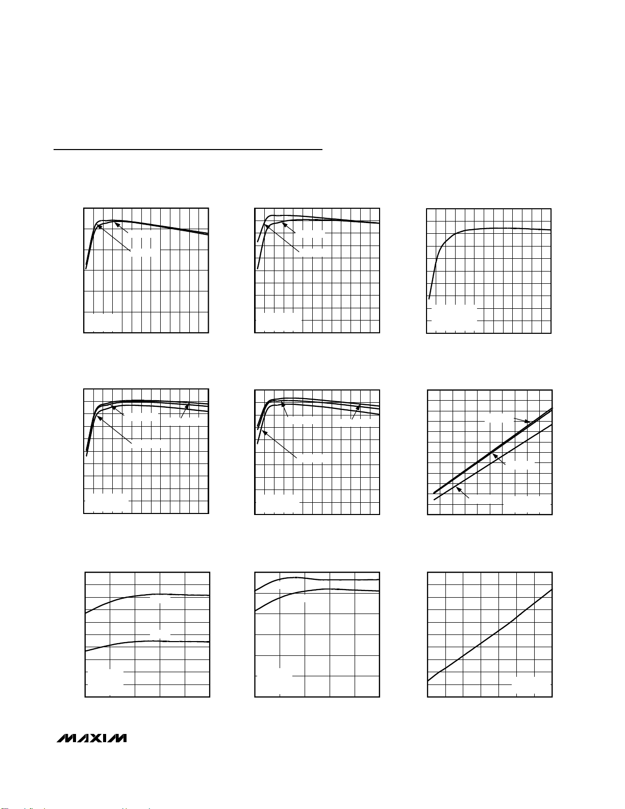
EFFICIENCY vs. OUTPUT CURRENT AND
EFFICIENCY vs. OUTPUT CURRENT
INTERNAL OSCILLATOR FREQUENCY
MAX5038A/41A toc01
η (%)
100
90
80
70
60
50
40
30
20
V
OUT
10
= 250kHz
f
SW
0
052
EFFICIENCY vs. OUTPUT CURRENT
100
90
80
70
η (%)
60
50
VIN = +5V
V
OUT
40
052
= +1.8V
f = 500kHz
f = 250kHz
I
(A)
OUT
4844403632282420161284
EFFICIENCY vs. OUTPUT CURRENT
AND OUTPUT VOLTAGE
100
90
80
70
60
50
η (%)
40
30
20
VIN = +12V
10
f
SW
0
052
= 250kHz
V
OUT
= +1.5V
V
OUT
I
OUT
= +1.1V
(A)
V
= +1.8V
OUT
4844403632282420161284
MAX5038A/41A toc04
η (%)
100
90
80
70
60
50
40
30
20
VIN = +5V
10
= 500kHz
f
SW
0
052
AND INPUT VOLTAGE
VIN = +12V
VIN = +5V
= +1.8V
I
(A)
OUT
AND OUTPUT VOLTAGE
V
= +1.5V
OUT
V
= +1.1V
OUT
I
(A)
OUT
EFFICIENCY vs. OUTPUT CURRENT
100
90
80
MAX5038A/41A toc02
70
60
50
η (%)
40
30
20
VIN = +24V
= +1.8V
V
OUT
10
= 125kHz
f
SW
4844403632282420161284
0
052
I
(A)
OUT
SUPPLY CURRENT
vs. FREQUENCY AND INPUT VOLTAGE
12.0
11.5
11.0
10.5
4844403632282420161284
MAX5038A/41A toc05
(mA)
CC
I
10.0
9.5
9.0
8.5
8.0
7.5
7.0
6.5
6.0
100 600
V
= +1.8V
OUT
VIN = +24V
VIN = +5V
FREQUENCY (kHz)
VIN = +12V
EXTERNALCLOCK
NO DRIVER LOAD
MAX5038A/41A toc03
4844403632282420161284
MAX5038A/41A toc06
550500400 450200 250 300 350150
SUPPLY CURRENT
vs. TEMPERATURE AND FREQUENCY
100
90
80
70
60
(mA)
50
CC
I
40
30
20
VIN = +12V
= 22nF
C
DL_
10
= 8.2nF
C
DH_
0
-40 85
250kHz
125kHz
TEMPERATURE (°C)
SUPPLY CURRENT
vs. TEMPERATURE AND FREQUENCY
175
150
MAX5038A/41A toc07
125
(mA)
100
CC
I
75
50
603510-15
25
600kHz
500kHz
VIN = +5V
= 22nF
C
DL_
= 8.2nF
C
DH_
-40 85
TEMPERATURE (°C)
603510-15
MAX5038A/41A toc08
(mA)
CC
I
100
90
80
70
60
50
40
30
20
10
0
115
SUPPLY CURRENT
vs. LOAD CAPACITANCE PER DRIVER
VIN = +12V
= 250kHz
f
SW
13117 953
C
(nF)
DRIVER
MAX5038A/41A toc09
Page 6
MAX5038A/MAX5041A
Dual-Phase, Parallelable, Average-Current-Mode
Controllers
6 _______________________________________________________________________________________
Typical Operating Characteristics (continued)
(Circuit of Figure 1, TA= +25°C, unless otherwise noted.)
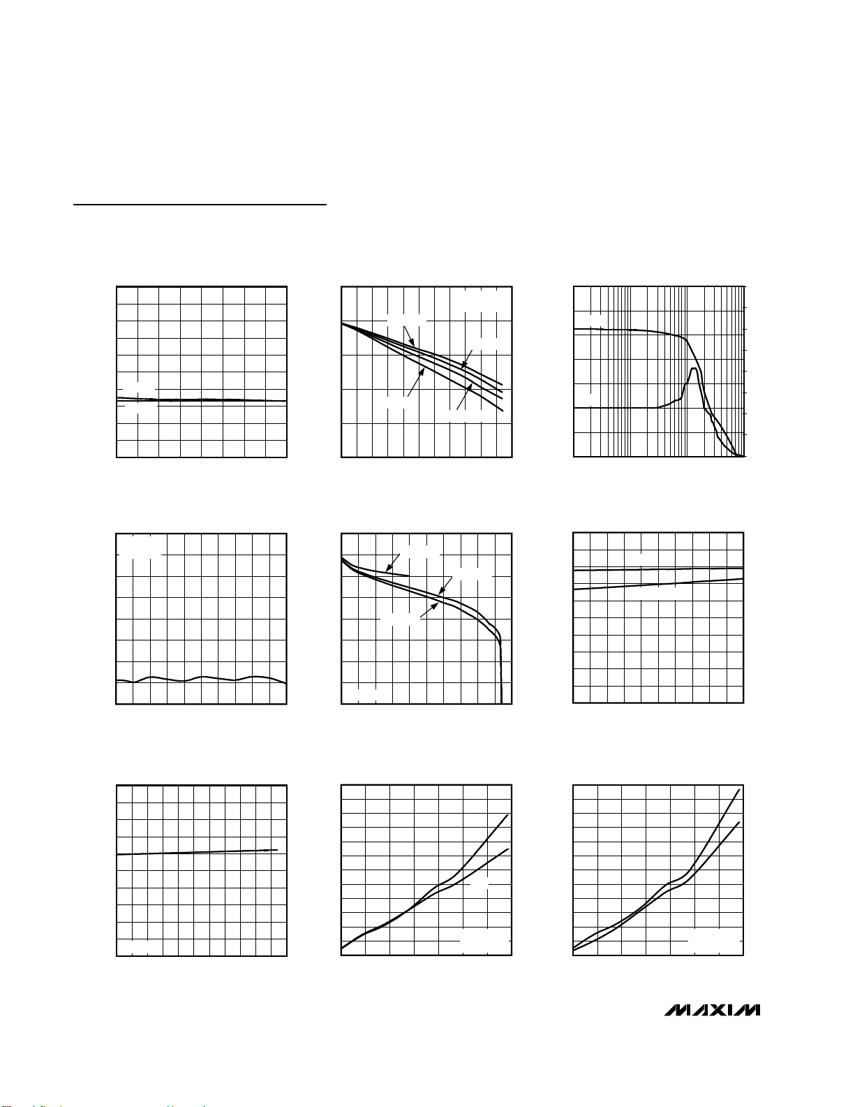
CURRENT-SENSE THRESHOLD
vs. OUTPUT VOLTAGE
MAX5038A/41A toc10
V
OUT
(V)
(V
CSP_
- V
CSN_
) (mV)
1.71.61.4 1.51.2 1.31.1
46
47
48
49
50
51
52
53
54
55
45
1.0 1.8
PHASE 2
PHASE 1
OUTPUT VOLTAGE vs. OUTPUT CURRENT
AND ERROR AMP GAIN (R
F
/ RIN)
MAX5038A/41A toc11
I
LOAD
(A)
V
OUT
(V)
5045403530252015105
1.65
1.70
1.75
1.80
1.85
1.60
055
VIN = +12V
V
OUT
= +1.8V
RF / RIN = 15
RF / RIN = 12.5
RF / RIN = 10
RF / RIN = 7.5
DIFFERENTIAL AMPLIFIER BANDWIDTH
MAX5038A/41A toc12
FREQUENCY (MHz)
GAIN (V/V)
PHASE (DEGREES)
10.1
0.5
1.0
1.5
2.0
2.5
3.0
3.5
0
0.01 10
-225
-270
-180
-135
-90
-45
0
45
90
PHASE
GAIN
DIFF OUTPUT ERROR
vs. SENSE+ TO SENSE- VOLTAGE
MAX5038A/41A toc13
∆V
SENSE
(V)
ERROR (%)
1.91.81.1 1.2 1.3 1.5 1.61.4 1.7
0.025
0.050
0.075
0.100
0.125
0.150
0.175
0.200
0
1.0 2.0
VIN = +12V
NO DRIVER
VCC LOAD REGULATION
vs. INPUT VOLTAGE
MAX5038A/41A toc14
ICC (mA)
V
CC
(V)
13512015 30 45 75 9060 105
4.85
4.90
4.95
5.00
5.05
5.10
5.15
5.20
4.80
0 150
VIN = +24V
VIN = +12V
VIN = +8V
DC LOAD
VCC LINE REGULATION
MAX5038A/41A toc15
VIN (V)
V
CC
(V)
262420 2212 14 16 1810
4.80
4.85
4.90
4.95
5.00
5.05
5.10
5.15
5.20
5.25
4.75
828
ICC = 0
ICC = 40mA
VCC LINE REGULATION
MAX5038A/41A toc16
VIN (V)
V
CC
(V)
131291011
4.80
4.85
4.90
4.95
5.00
5.05
5.10
5.15
5.20
5.25
4.75
8
ICC = 80mA
DRIVER RISE TIME
vs. DRIVER LOAD CAPACITANCE
MAX5038A/41A toc17
C
DRIVER
(nF)
t
R
(ns)
312616 21116
10
20
30
40
50
60
70
80
90
100
110
120
0
136
DL_
DH_
VIN = +12V
f
SW
= 250kHz
DRIVER FALL TIME
vs. DRIVER LOAD CAPACITANCE
MAX5038A/41A toc18
C
DRIVER
(nF)
t
F
(ns)
312616 21116
10
20
30
40
50
60
70
80
90
100
110
120
0
136
DL_
DH_
VIN = +12V
f
SW
= 250kHz
Page 7
MAX5038A/MAX5041A
Dual-Phase, Parallelable, Average-Current-Mode
Controllers
_______________________________________________________________________________________ 7
Typical Operating Characteristics (continued)
(Circuit of Figure 1, TA= +25°C, unless otherwise noted.)
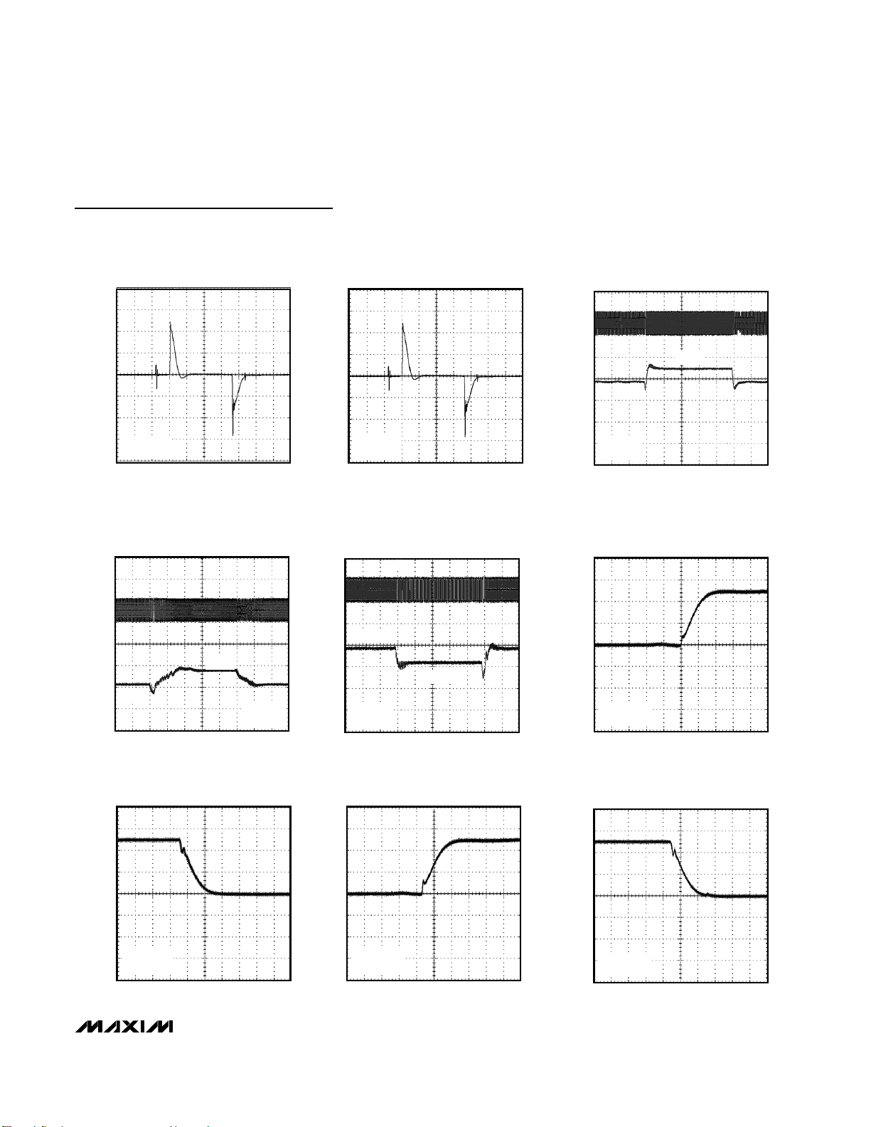
HIGH-SIDE DRIVER (DH_)
DH_
1.6A/div
CLKOUT
5V/div
PLLCMP
200mV/div
SINK AND SOURCE CURRENT
VIN = +12V
= 22nF
C
DH_
100ns/div
PLL LOCKING TIME
250kHz TO 500kHz AND
500kHz TO 250kHz
250kHz
0
100
µs/div
500kHz
MAX5038A/41A toc19
MAX5038A/41A toc22
VIN = +12V
NO LOAD
DL_
1.6A/div
CLKOUT
5V/div
PLLCMP
200mV/div
0
VIN = +12V
C
DL_
250kHz
VIN = +12V
NO LOAD
LOW-SIDE DRIVER (DL_)
SINK AND SOURCE CURRENT
= 22nF
100ns/div
MAX5038A/41A toc20
PLL LOCKING TIME
250kHz TO 150kHz AND
150kHz TO 250kHz
100
MAX5038A/41A toc23
150kHz
µs/div
CLKOUT
5V/div
PLLCMP
200mV/div
PLL LOCKING TIME
250kHz TO 350kHz AND
350kHz TO 250kHz
250kHz
0
VIN = +12V
NO LOAD
HIGH-SIDE DRIVER (DH_)
VIN = +12V
= 22nF
C
DH_
350kHz
100
µs/div
RISE TIME
40ns/div
MAX5038A/41A toc21
MAX5038A/41A toc24
DH_
2V/div
HIGH-SIDE DRIVER (DH_)
FALL TIME
VIN = +12V
= 22nF
C
DH_
40ns/div
MAX5038A/41A toc25
DH_
2V/div
LOW-SIDE DRIVER (DL_)
RISE TIME
VIN = +12V
= 22nF
C
DL_
40ns/div
MAX5038A/41A toc26
DL_
2V/div
LOW-SIDE DRIVER (DL_)
FALL TIME
VIN = +12V
= 22nF
C
DL_
40ns/div
MAX5038A/41A toc27
DL_
2V/div
Page 8
MAX5038A/MAX5041A
Dual-Phase, Parallelable, Average-Current-Mode
Controllers
8 _______________________________________________________________________________________
Typical Operating Characteristics (continued)
(Circuit of Figure 1, TA= +25°C, unless otherwise noted.)
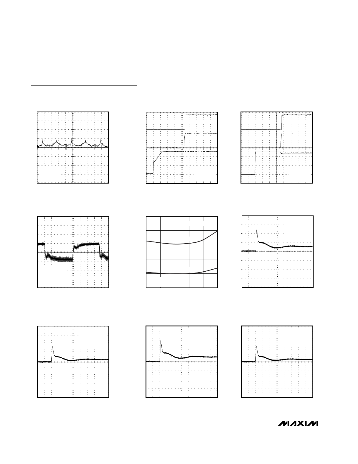
500ns/div
OUTPUT RIPPLE
MAX5038A/41A toc28
V
OUT
(AC-COUPLED)
10mV/div
VIN = +12V
V
OUT
= +1.75V
I
OUT
= 52A
2ms/div
INPUT STARTUP RESPONSE
MAX5038A/41A toc29
VIN
5V/div
VIN = +12V
V
OUT
= +1.75V
I
OUT
= 52A
V
PGOOD
1V/div
V
OUT
1V/div
1ms/div
ENABLE STARTUP RESPONSE
MAX5038A/41A toc30
VEN
2V/div
V
PGOOD
1V/div
V
OUT
1V/div
VIN = +12V
V
OUT
= +1.75V
I
OUT
= 52A
40
µs/div
LOAD-TRANSIENT RESPONSE
MAX5038A/41A toc31
VIN = +12V
V
OUT
= +1.75V
I
STEP
= 8A TO 52A
t
RISE
= 1µs
V
OUT
50mV/div
REVERSE-CURRENT SINK vs.
TEMPERATURE
MAX5038A/41A toc32
TEMPERATURE (°C)
I
REVERSE
(A)
603510-15
2.4
2.5
2.6
2.7
2.8
2.3
-40 85
V
EXTERNAL
= +3.3V
R1 = R2 = 1.5mΩ
V
EXTERNAL
= +2V
VIN = +12V
V
OUT
= +1.5V
200
µs/div
REVERSE-CURRENT SINK
AT INPUT TURN-ON
MAX5038A/41A toc33
VIN = +12V
V
OUT
= +1.5V
V
EXTERNAL
= 2.5V
R1 = R2 = 1.5mΩ
REVERSE
CURRENT
5A/div
0A
200µs/div
REVERSE-CURRENT SINK
AT INPUT TURN-ON
MAX5038A/41A toc34
VIN = +12V
V
OUT
= +1.5V
V
EXTERNAL
= 3.3V
R1 = R2 = 1.5mΩ
REVERSE
CURRENT
10A/div
0A
200µs/div
REVERSE-CURRENT SINK
AT ENABLE TURN-ON
MAX5038A/41 toc35
VIN = +12V
V
OUT
= +1.5V
V
EXTERNAL
= 2.5V
R1 = R2 = 1.5mΩ
REVERSE
CURRENT
5A/div
0A
200µs/div
REVERSE-CURRENT SINK
AT ENABLE TURN-ON
MAX5038A/41 toc36
VIN = +12V
V
OUT
= +1.5V
V
EXTERNAL
= 3.3V
R1 = R2 = 1.5mΩ
REVERSE
CURRENT
10A/div
0A
Page 9

MAX5038A/MAX5041A
Dual-Phase, Parallelable, Average-Current-Mode
Controllers
_______________________________________________________________________________________ 9
Pin Description
PIN NAME FUNCTION
1, 13
2, 14
3 PHASE
4 PLLCMP
5, 7
6 SGND Signal Ground. Ground connection for the internal control circuitry.
8 SENSE+
9 SENSE-
10 DIFF Differential Remote-Sense Amplifier Output. DIFF is the output of a precision unity-gain amplifier.
11 EAN
12 EAOUT
15 EN Output Enable. A logic low shuts down the power drivers. EN has an internal 5µA pullup current.
16, 26
17, 25
18, 24 LX1, LX2
19, 23
20 V
21 IN
22 PGND
27 CLKOUT
28 CLKIN
CSP2,
CSP1
CSN2,
CSN1
CLP2,
CLP1
BST1,
BST2
DH1,
DH2
DL1,
DL2
CC
Current-Sense Differential Amplifier Positive Input. Senses the inductor current. The differential voltage
between CSP_ and CSN_ is amplified internally by the current-sense amplifier gain of 18.
Current-Sense Differential Amplifier Negative Input. Together with CSP_, senses the inductor current.
Phase-Shift Setting Input. Connect PHASE to V
PHASE to SGND for 60° of phase shift between the rising edges of CLKOUT and CLKIN/DH1.
External Loop-Compensation Input. Connect compensation network for the phase-locked loop (see Phase-
Locked Loop section).
Current-Error Amplifier Output. Compensate the current loop by connecting an RC network to ground.
Differential Output Voltage-Sensing Positive Input. Used to sense a remote load. Connect SENSE+ to
at the load. The MAX5038A regulates the difference between SENSE+ and SENSE- according to the
V
OUT+
factory preset output voltage. The MAX5041A regulates the SENSE+ to SENSE- difference to +1.0V.
Differential Output Voltage-Sensing Negative Input. Used to sense a remote load. Connect SENSE- to
V
or PGND at the load.
OUT-
Voltage-Error Amplifier Inverting Input. Receives the output of the differential remote-sense amplifier.
Referenced to SGND.
Voltage-Error Amplifier Output. Connect to the external gain-setting feedback resistor. The external error
amplifier gain-setting resistors determine the amount of adaptive voltage positioning
Boost Flying-Capacitor Connection. Reservoir capacitor connection for the high-side FET driver supply.
Connect a 0.47µF ceramic capacitor between BST_ and LX_.
High-Side Gate Driver Output. Drives the gate of the high-side MOSFET.
Inductor Connection. Source connection for the high-side MOSFETs. Also serves as the return terminal for
the high-side driver.
Low-Side Gate Driver Output. Synchronous MOSFET gate drivers for the two phases.
Internal +5V Regulator Output. VCC is derived internally from the IN voltage. Bypass to SGND with 4.7µF
and 0.1µF ceramic capacitors.
Supply Voltage Connection. Connect IN to V
RC lowpass filter, a 2.2Ω resistor, and a 0.1µF ceramic capacitor.
Power Ground. Connect PGND, low-side synchronous MOSFET’s source, and V
together.
Oscillator Output. CLKOUT is phase shifted from CLKIN by the amount specified by PHASE. Use CLKOUT
to parallel additional MAX5038A/MAX5041As.
CMOS Logic Clock Input. Drive the internal oscillator with a frequency range between 125kHz and 600kHz,
or connect to V
V
to set the internal oscillator to 500kHz. CLKIN has an internal 5µA pulldown current.
CC
or SGND. Connect CLKIN to SGND to set the internal oscillator to 250kHz or connect to
CC
for 120°, leave PHASE unconnected for 90°, or connect
CC
for a +5V system. Connect the VRM input to IN through an
CC
bypass capacitor returns
CC
Page 10

MAX5038A/MAX5041A
Dual-Phase, Parallelable, Average-Current-Mode
Controllers
10 ______________________________________________________________________________________
Functional Diagram
EN
IN
V
CC
CSP1
CSN1
CLP1
SGND
+5V
LDO
REGULATOR
TO INTERNAL CIRCUITS
UVLO
POR
TEMP SENSOR
MAX5038A
MAX5041A
DIFF
AMP
PHASE-
LOCKED
LOOP
0.6V
ERROR
AMP
RAMP
GENERATOR
CLKIN
PHASE
CLKOUT
PLLCMP
DIFF
SENSE-
SENSE+
EAOUT
EAN
CSP1
CSN1
CLP1
CLK
GM
DRV_V
PHASE 1
IN
RAMP1
SHDN
CC
PGND
BST1
DH1
LX1
DL1
PGND
CC
PHASE 2
SHDN
PGND
CLP2
CSN2
CSP2
V
= V
for V
REF
OUT
= V
/2 for V
V
REF
OUT
= +1.0V (MAX5041A)
V
REF
1.8V (MAX5038A)
OUT ≤
> 1.8V (MAX5038A)
OUT
CLK
RAMP2
GM
IN
CLP2
CSN2
CSP2
DRV_V
DH2
LX2
DL2
BST2
Page 11

MAX5038A/MAX5041A
Dual-Phase, Parallelable, Average-Current-Mode
Controllers
______________________________________________________________________________________ 11
Detailed Description
The MAX5038A/MAX5041A (Figures 1 and 2) averagecurrent-mode PWM controllers drive two out-of-phase
buck converter channels. Average-current-mode control improves current sharing between the channels
while minimizing component derating and size. Parallel
multiple MAX5038A/MAX5041A regulators to increase
the output current capacity. For maximum ripple rejection at the input, set the phase shift between phases to
90° for two paralleled converters, or 60° for three paralleled converters. The paralleling capability of the
MAX5038A/MAX5041A improves design flexibility in
applications requiring upgrades (higher load).
Figure 1. MAX5038A Typical Application Circuit, VIN= +12V
9
SENSE-
8
SENSE+
CSN1
CSP1
DH1
LX1
DL1
BST1
V
DH2
LX2
DL2
BST2
14
13
17
18
19
16
20
CC
25
24
23
26
C1, C2
V
CC
3
PHASE
15
C39
EN
21
IN
28
CLKIN
V
= +12V
IN
V
R1
CC
MAX5038A
4
10
11
12
7
5
PLLCMP
DIFF
EAN
EAOUT
CLP1
CLP2
C25
C26
R
X
C29
R4
R7
R8
R6
C30
C28
V
IN
C3–C7
C32
Q1
Q2
D1
C34
V
IN
C8–C11
Q1
Q2
D2
L1
C12
C31
L2
C13
R2
D3
D4
R3
C14,
C15
+1.8V AT 60A
C16–C24,
C33
V
OUT
LOAD
R5
C27
6
SGND
22
PGND
CSP2
CSN2
1
2
NOTE: SEE TABLE 1 FOR COMPONENT VALUES.
Page 12

MAX5038A/MAX5041A
Dual-Phase, Parallelable, Average-Current-Mode
Controllers
12 ______________________________________________________________________________________
Dual-phase converters with an out-of-phase locking
arrangement reduce the input and output capacitor
ripple current, effectively multiplying the switching frequency by the number of phases. Each phase of the
MAX5038A/MAX5041A consists of an inner average
current loop controlled by a common outer-loop volt-
age-error amplifier (VEA). The combined action of the
two inner current loops and the outer voltage loop corrects the output voltage errors and forces the phase
currents to be equal.
Figure 2. MAX5041A Typical Application Circuit, VIN= +12V
9
SENSE-
8
SENSE+
3
PHASE
15
C39
EN
21
IN
28
CLKIN
V
= +12V
IN
C1,
C2
V
R1
CC
MAX5041A
4
10
11
12
7
5
PLLCMP
DIFF
EAN
EAOUT
CLP1
CLP2
C25
C26
V
CC
R
X
C29
R4
R7
R8
R6
C30
C28
CSN1
CSP1
DH1
LX1
DL1
BST1
V
DH2
LX2
DL2
BST2
14
13
17
18
19
16
20
CC
25
24
23
26
C32
V
IN
C3–C7
Q1
Q2
D1
C34
V
IN
C8–C11
Q1
Q2
D2
L1
C12
C31
L2
C13
R2
D3
+1.8V AT 60A
V
D4
R3
C14,
C15
C16–C24,
C33
LOAD
OUT
R
H
R
L
R5
C27
6
SGND
22
PGND
CSP2
CSN2
1
2
NOTE: SEE TABLE 1 FOR COMPONENT VALUES.
Page 13

MAX5038A/MAX5041A
Dual-Phase, Parallelable, Average-Current-Mode
Controllers
______________________________________________________________________________________ 13
VINand V
CC
The MAX5038A/MAX5041A accept an input voltage
range of +4.75V to +5.5V or +8V to +28V. All internal
control circuitry operates from an internally regulated
nominal voltage of +5V (VCC). For input voltages of +8V
or greater, the internal VCCregulator steps the voltage
down to +5V. The VCCoutput voltage is a regulated +5V
output capable of sourcing up to 80mA. Bypass VCCto
SGND with 4.7µF and 0.1µF low-ESR ceramic capacitors
in parallel for high-frequency noise rejection and stable
operation (Figures 1 and 2).
Calculate power dissipation in the MAX5038A/
MAX5041A as a product of the input voltage and the
total VCCregulator output current (ICC). ICCincludes
quiescent current (IQ) and gate drive current (IDD):
PD = V
IN
x I
CC
ICC= IQ+ fSWx (QG1+ Q
G2
+ QG3+ QG4)
where QG1, QG2, Q
G3,
and QG4are the total gate
charge of the low-side and high-side external
MOSFETs, IQis 4mA (typ), and fSWis the switching frequency of each individual phase.
For applications utilizing a +5V input voltage, disable
the VCCregulator by connecting IN and VCCtogether.
Undervoltage Lockout (UVLO)/Soft-Start
The MAX5038A/MAX5041A include an undervoltage
lockout with hysteresis and a power-on reset circuit for
converter turn-on and monotonic rise of the output voltage. The UVLO threshold is internally set between
+4.0V and +4.5V with a 200mV hysteresis. Hysteresis
at UVLO eliminates “chattering” during startup.
Most of the internal circuitry, including the oscillator,
turns on when the input voltage reaches +4V. The
MAX5038A/MAX5041A draw up to 4mA of current before
the input voltage reaches the UVLO threshold.
The compensation network at the current-error amplifiers (CLP1 and CLP2) provides an inherent soft-start of
the output voltage. It includes a parallel combination of
capacitors (C28, C30) and resistors (R5, R6) in series
with other capacitors (C27, C29) (see Figures 1 and 2).
The voltage at CLP_ limits the maximum current available to charge output capacitors. The capacitor on
CLP_ in conjunction with the finite output-drive current
of the current-error amplifier yields a finite rise time for
the output current and thus the output voltage.
Internal Oscillator
The internal oscillator generates the 180° out-of-phase
clock signals required by the pulse-width modulation
(PWM) circuits. The oscillator also generates the 2V
P-P
voltage ramp signals necessary for the PWM comparators. Connect CLKIN to SGND to set the internal oscillator
frequency to 250kHz or connect CLKIN to VCCto set the
internal oscillator to 500kHz.
CLKIN is a CMOS logic clock input for the phaselocked loop (PLL). When driven externally, the internal
oscillator locks to the signal at CLKIN. A rising edge at
CLKIN starts the ON cycle of the PWM. Ensure that the
external clock pulse width is at least 200ns. CLKOUT
provides a phase-shifted output with respect to the rising edge of the signal at CLKIN. PHASE sets the
amount of phase shift at CLKOUT. Connect PHASE to
VCCfor 120° of phase shift, leave PHASE unconnected
for 90° of phase shift, or connect PHASE to SGND for
60° of phase shift with respect to CLKIN.
The MAX5038A/MAX5041A require compensation on
PLLCMP even when operating from the internal oscillator.
The device requires an active PLL in order to generate
the proper clock signal required for PWM operation.
Control Loop
The MAX5038A/MAX5041A use an average-currentmode control scheme to regulate the output voltage
(Figures 3a and 3b). The main control loop consists of
an inner current loop and an outer voltage loop. The
inner loop controls the output currents (I
PHASE1
and
I
PHASE2
) while the outer loop controls the output voltage. The inner current loop absorbs the inductor pole
reducing the order of the outer voltage loop to that of a
single-pole system.
The current loop consists of a current-sense resistor
(RS), a current-sense amplifier (CA_), a current-error
amplifier (CEA_), an oscillator providing the carrier
ramp, and a PWM comparator (CPWM_). The precision
CA_ amplifies the sense voltage across RSby a factor
of 18. The inverting input to the CEA_ senses the CA_
output. The CEA_ output is the difference between the
voltage-error amplifier output (EAOUT) and the amplified voltage from the CA_. The RC compensation network connected to CLP1 and CLP2 provides external
frequency compensation for the respective CEA_. The
start of every clock cycle enables the high-side drivers
and initiates a PWM ON cycle. Comparator CPWM_
compares the output voltage from the CEA_ with a 0 to
+2V ramp from the oscillator. The PWM ON cycle terminates when the ramp voltage exceeds the error voltage.
(1)
(2)
Page 14

MAX5038A/MAX5041A
Dual-Phase, Parallelable, Average-Current-Mode
Controllers
14 ______________________________________________________________________________________
Figure 3b. MAX5041A Control Loop
Figure 3a. MAX5038A Control Loop
C
CF
R
CF
C
CSP1
CLP1
CFF
CSN1
MAX5038A
SENSE+
SENSE-
*RF AND RIN ARE EXTERNAL TO MAX5038A
= R8, RIN = R7, FIGURE 1).
(R
F
RIN*
DIFF
AMP
CA1
R
*
F
VEA
V
REF
CSN2
CEA1
CEA2
CA2
CSP2
CSN1
CSP1
CLP2
CLP1
CPWM1
CPWM2
R
CF
R
V
IN
I
DRIVE 1
DRIVE 2
C
CF
C
CCF
C
CF
CF
C
CFF
PHASE1
R
S
V
OUT
V
IN
C
OUT
R
I
PHASE2
S
LOAD
SENSE+
SENSE-
*RF AND RIN ARE
EXTERNAL TO MAX5041A
= R8, RIN = R7, FIGURE 2).
(R
F
DIFF
AMP
MAX5041A
RIN*
V
+1.0V
CA1
R
*
F
VEA
=
REF
CSN2
CEA1
CEA2
CA2
CLP2
CSP2
CPWM1
CPWM2
R
CF
DRIVE 1
DRIVE 2
C
CF
C
CCF
V
IN
I
PHASE1
R
S
V
V
IN
I
PHASE2
OUT
C
OUT
R
S
LOAD
Page 15

MAX5038A/MAX5041A
Dual-Phase, Parallelable, Average-Current-Mode
Controllers
______________________________________________________________________________________ 15
The outer voltage control loop consists of the differential amplifier (DIFF AMP), reference voltage, and VEA.
The unity-gain differential amplifier provides true differential remote sensing of the output voltage. The differential amplifier output connects to the inverting input
(EAN) of the VEA. The noninverting input of the VEA is
internally connected to an internal precision reference
voltage. The MAX5041A reference voltage is set to
+1.0V and the MAX5038A reference is set to the preset
output voltage. The VEA controls the two inner current
loops (Figures 3a and 3b). Use a resistive feedback
network to set the VEA gain as required by the adaptive
voltage-positioning circuit (see the Adaptive Voltage
Positioning section).
Current-Sense Amplifier
The differential current-sense amplifier (CA_) provides a
DC gain of 18. The maximum input offset voltage of the
current-sense amplifier is 1mV and the common-mode
voltage range is -0.3V to +3.6V. The current-sense amplifier senses the voltage across a current-sense resistor.
Peak-Current Comparator
The peak-current comparator provides a path for fast
cycle-by-cycle current limit during extreme fault conditions such as an output inductor malfunction (Figure 4).
Note that the average-current-limit threshold of 48mV
still limits the output current during short-circuit conditions. To prevent inductor saturation, select an output
inductor with a saturation current specification greater
than the average current limit (48mV). Proper inductor
selection ensures that only extreme conditions trip the
peak-current comparator, such as a broken output
inductor. The 112mV voltage threshold for triggering
the peak-current limit is twice the full-scale average
current-limit voltage threshold. The peak-current comparator has a delay of only 260ns.
Current-Error Amplifier
Each phase of the MAX5038A/MAX5041A has a dedicated transconductance current-error amplifier (CEA_)
with a typical gmof 550µS and 320µA output sink and
source current capability. The current-error amplifier
outputs, CLP1 and CLP2, serve as the inverting input to
the PWM comparator. CLP1 and CLP2 are externally
accessible to provide frequency compensation for the
inner current loops (Figures 3a and 3b). Compensate
CEA_ such that the inductor current down slope, which
becomes the up slope to the inverting input of the PWM
comparator, is less than the slope of the internally generated voltage ramp (see the Compensation section).
PWM Comparator and R-S Flip-Flop
The PWM comparator (CPWM) sets the duty cycle for
each cycle by comparing the output of the current-error
amplifier to a 2V
P-P
ramp. At the start of each clock
cycle, an R-S flip-flop resets and the high-side driver
(DH_) turns on. The comparator sets the flip-flop as
soon as the ramp voltage exceeds the CLP_ voltage,
thus terminating the ON cycle (Figure 4).
Figure 4. Phase Circuit (Phase 1/Phase 2)
DRV_V
CC
CLP_
CSP_
CSN_
GM
IN
RAMP
2 x fs (V/s)
CLK
SHDN
112mV
= 18
A
V
PEAK-CURRENT
COMPARATOR
Gm =
550µS
PWM
COMPARATOR
BST_
S
R
Q
Q
DH_
LX_
DL_
PGND
Page 16

MAX5038A/MAX5041A
Dual-Phase, Parallelable, Average-Current-Mode
Controllers
16 ______________________________________________________________________________________
Differential Amplifier
The differential amplifier (DIFF AMP) facilitates output
voltage remote sensing at the load (Figures 3a and 3b).
It provides true differential output voltage sensing while
rejecting the common-mode voltage errors due to highcurrent ground paths. Sensing the output voltage
directly at the load provides accurate load voltage
sensing in high-current environments. The VEA provides the difference between the differential amplifier
output (DIFF) and the desired output voltage. The differential amplifier has a bandwidth of 3MHz. The difference between SENSE+ and SENSE- regulates to the
preset output voltage for the MAX5038A and regulates
to +1V for the MAX5041A.
Voltage-Error Amplifier
The VEA sets the gain of the voltage control loop and
determines the error between the differential amplifier
output and the internal reference voltage (V
REF
).
V
REF
equals V
OUT(NOM)
for the +1.8V or lower voltage
versions of the MAX5038A and V
REF
equals V
OUT(NOM)
/2
for the +2.5V and +3.3V versions. For MAX5041A, V
REF
equals +1V.
An offset is added to the output voltage of the
MAX5038A/MAX5041A with a finite gain (RF/RIN) of the
VEA such that the no-load output voltage is higher than
the nominal value. Choose RFand RINfrom the
Adaptive Voltage Positioning section and use the following equations to calculate the no-load output voltage.
MAX5038A:
MAX5041A:
where RHand RLare the feedback resistor network
(Figure 2).
Some applications require V
OUT
equal to V
OUT(NOM)
at
no load. To ensure that the output voltage does not
exceed the nominal output voltage (V
OUT(NOM)
), add a
resistor RXfrom VCCto EAN.
Use the following equations to calculate the value of R
X
.
For MAX5038A versions of V
OUT(NOM)
≤ +1.8V:
For MAX5038A versions of V
OUT(NOM)
> +1.8V:
For MAX5041A:
The VEA output clamps to +0.9V (plus the commonmode voltage of +0.6V), thus limiting the average maximum current from individual phases. The maximum
average-current-limit threshold for each phase is equal
to the maximum clamp voltage of the VEA divided by
the gain (18) of the current-sense amplifier. This allows
for accurate settings for the average maximum current
for each phase. Set the VEA gain using RFand RINfor
the amount of output voltage positioning required as
discussed in the Adaptive Voltage Positioning section
(Figures 3a and 3b).
Adaptive Voltage Positioning
Powering new-generation processors requires new
techniques to reduce cost, size, and power dissipation.
Voltage positioning reduces the total number of output
capacitors to meet a given transient response requirement. Setting the no-load output voltage slightly higher
than the output voltage during nominally loaded conditions allows a larger downward voltage excursion when
the output current suddenly increases. Regulating at a
lower output voltage under a heavy load allows a larger
upward-voltage excursion when the output current suddenly decreases. A larger allowed, voltage-step excursion reduces the required number of output capacitors
or allows for the use of higher ESR capacitors.
Voltage positioning and the ability to operate with multiple
reference voltages may require the output to regulate
away from a center value. Define the center value as the
voltage where the output drops (∆V
OUT
/2) at one half the
maximum output current (Figure 5).
(3)
(4)
(5)
(6)
(7)
V
OUT NL
V
OUT NL
=+
R
=+
R
IN
×1
V
F
RR
HL
×
OUT NOM() ( )
+
×1
V
R
L
REF()
R
IN
R
F
RV V
=− +×[( .)]06
X CC NOM
RVV
=− +×[( .)]212
X CC NOM
RV
=−×[.]16
XCC
V
R
REF
R
V
NOM
V
F
F
R
F
Page 17

MAX5038A/MAX5041A
Dual-Phase, Parallelable, Average-Current-Mode
Controllers
______________________________________________________________________________________ 17
Set the voltage-positioning window (∆V
OUT
) using the
resistive feedback of the VEA. Use the following equations to calculate the voltage-positioning window for the
MAX5038A:
Use the following equation to calculate the voltage-positioning window for the MAX5041A:
where R
IN
and RFare the input and feedback resistors of
the VEA, GCis the current-loop transconductance, and
R
S
is the current-sense resistor or, if using lossless induc-
tor current sensing, the DC resistance of the inductor.
Phase-Locked Loop: Operation and
Compensation
The PLL synchronizes the internal oscillator to the external frequency source when driving CLKIN. Connecting
CLKIN to VCCor SGND forces the PWM frequency to
default to the internal oscillator frequency of 500kHz or
250kHz, respectively. The PLL uses a conventional
architecture consisting of a phase detector and a
charge pump capable of providing 20µA of output current. Connect an external series combination capacitor
(C25) and resistor (R4) and a parallel capacitor (C26)
from PLLCMP to SGND to provide frequency compensation for the PLL (Figure 1). The pole-zero pair compensation provides a zero at fZdefined by 1 / [R4 x
(C25 + C26)] and a pole at fPdefined by 1 / (R4 x C26).
Use the following typical values for compensating the
PLL: R4 = 7.5kΩ, C25 = 4.7nF, C26 = 470pF. If changing the PLL frequency, expect a finite locking time of
approximately 200µs.
The MAX5038A/MAX5041A require compensation on
PLLCMP even when operating from the internal oscillator. The device requires an active PLL in order to generate the proper internal PWM clocks.
MOSFET Gate Drivers (DH_, DL_)
The high-side (DH_) and low-side (DL_) drivers drive
the gates of external N-channel MOSFETs (Figures 1
and 2). The drivers’ high-peak sink and source current
capability provides ample drive for the fast rise and fall
times of the switching MOSFETs. Faster rise and fall
times result in reduced cross-conduction losses. For
modern CPU voltage-regulating module applications
where the duty cycle is less than 50%, choose highside MOSFETs (Q1 and Q3) with a moderate R
DS(ON)
and a very low gate charge. Choose low-side MOSFETs
(Q2 and Q4) with very low R
DS(ON)
and moderate gate
charge.
The driver block also includes a logic circuit that provides an adaptive nonoverlap time to prevent shootthrough currents during transition. The typical
nonoverlap time is 60ns between the high-side and lowside MOSFETs.
BST_
VCCpowers the low- and high-side MOSFET drivers.
Connect a 0.47µF low-ESR ceramic capacitor between
BST_ and LX_. Bypass V
CC
to SGND with 4.7µF and
0.1µF low-ESR ceramic capacitors. For high-current
applications, bypass VCCto PGND with one or more
0.1µF, low-ESR ceramic capacitor(s). Reduce the PC
board area formed by these capacitors, the rectifier
diodes between VCCand the boost capacitor, the
MAX5038A/MAX5041A, and the switching MOSFETs.
Figure 5. Defining the Voltage-Positioning Window
(8)
(9)
(10)
(11)
VOLTAGE-POSITIONING WINDOW
V
+ ∆V
/2
CNTR
OUT
V
CNTR
V
- ∆V
/2
CNTR
OUT
FULL LOAD
NO LOAD
1/2 LOAD
LOAD (A)
IR
×
G
C
OUT IN
=
××2
005.
=
R
GR
CF
S
∆V
OUT
IR
×
∆V
OUT
OUT IN
=
GR
2
××
()
CF
005.
G
=
C
R
S
RR
+
HL
×
R
L
Page 18

MAX5038A/MAX5041A
Dual-Phase, Parallelable, Average-Current-Mode
Controllers
18 ______________________________________________________________________________________
Overload Conditions
Average-current-mode control has the ability to limit the
average current sourced by the converter during a fault
condition. When a fault condition occurs, the VEA output clamps to +0.9V with respect to the common-mode
voltage (VCM= +0.6V) and is compared with the output
of the current-sense amplifiers (CA1 and CA2) (see
Figures 3a and 3b). The current-sense amplifier’s gain
of 18 limits the maximum current in the inductor or
sense resistor to I
LIMIT
= 50mV/RS.
Parallel Operation
For applications requiring large output current, parallel
up to three MAX5038A/MAX5041As (six phases) to triple
the available output current. The paralleled converters
operate at the same switching frequency but different
phases keep the capacitor ripple RMS currents to a minimum. Three parallel MAX5038A/MAX5041A converters
deliver up to 180A of output current. To set the phase
shift of the on-board PLL, leave PHASE unconnected for
90° of phase shift (two paralleled converters), or connect
PHASE to SGND for 60° of phase shift (three converters
in parallel). Designate one converter as master and the
remaining converters as slaves. Connect the master and
slave controllers in a daisy-chain configuration as shown
in Figure 6. Connect CLKOUT from the master controller
to CLKIN of the first slaved controller, and CLKOUT from
the first slaved controller to CLKIN of the second slaved
controller. Choose the appropriate phase shift for minimum ripple currents at the input and output capacitors.
The master controller senses the output differential voltage through SENSE+ and SENSE- and generates the
DIFF voltage. Disable the voltage sensing of the slaved
controllers by leaving DIFF unconnected (floating).
Figure 7 shows a detailed typical parallel application circuit using two MAX5038As. This circuit provides four
phases at an input voltage of +12V and an output voltage range of +1V to +3.3V at 104A.
Applications Information
Each MAX5038A/MAX5041A circuit drives two 180° outof-phase channels. Parallel two or three MAX5038A/
MAX5041A circuits to achieve four- or six-phase operation, respectively. Figure 1 shows the typical application
circuit for a two-phase operation. The design criteria for
a two-phase converter includes frequency selection,
inductor value, input/output capacitance, switching
MOSFETs, sense resistors, and the compensation network. Follow the same procedure for the four- and sixphase converter design, except for the input and output
capacitance. The input and output capacitance requirements vary depending on the operating duty cycle.
The examples discussed in this data sheet pertain to a
typical application with the following specifications:
V
IN
= +12V
V
OUT
= +1.8V
I
OUT(MAX)
= 52A
fSW= 250kHz
Peak-to-Peak Inductor Current (∆I
L
) = 10A
Table 1 shows a list of recommended external components (Figure 1) and Table 2 provides component supplier information.
Number of Phases
Selecting the number of phases for a voltage regulator
depends mainly on the ratio of input-to-output voltage
(operating duty cycle). Optimum output-ripple cancellation depends on the right combination of operating duty
cycle and the number of phases. Use the following
equation as a starting point to choose the number of
phases:
NPH≈ K/D
where K = 1, 2, or 3 and the duty cycle is D = V
OUT/VIN.
Choose K to make NPHan integer number. For example, converting VIN= +12V to V
OUT
= +1.8V yields
better ripple cancellation in the six-phase converter
than in the four-phase converter. Ensure that the output
load justifies the greater number of components for
multiphase conversion. Generally limiting the maximum
output current to 25A per phase yields the most costeffective solution. The maximum ripple cancellation
occurs when NPH= K/D.
Single-phase conversion requires greater size and power
dissipation for external components such as the switching MOSFETs and the inductor. Multiphase conversion
eliminates the heatsink by distributing the power dissipation in the external components. The multiple phases
operating at given phase shifts effectively increase the
switching frequency seen by the input/output capacitors,
thereby reducing the input/output capacitance requirement for the same ripple performance. The lower inductance value improves the large-signal response of the
converter during a transient load at the output. Consider
all these issues when determining the number of phases
necessary for the voltage regulator application.
Inductor Selection
The switching frequency per phase, peak-to-peak ripple current in each phase, and allowable ripple at the
output determine the inductance value.
(12)
Page 19

MAX5038A/MAX5041A
Dual-Phase, Parallelable, Average-Current-Mode
Controllers
______________________________________________________________________________________ 19
Figure 6. Parallel Configuration of Multiple MAX5038A/MAX5041As
CSN1
MAX5038A/
MAX5041A
V
CC
CSP1
V
IN
DH1
LX1
DL1
V
IN
DH2
LX2
DL2
CSP2
CSN2
CLKOUTSGNDPGND
CSN1
CLKIN
PHASE
CSP1
DH1
V
IN
LX1
DL1
SENSE+
SENSE-
V
CC
PHASE
V
CC
CLKIN
V
IN
IN
DIFF
EAN
EAOUT
*FOR MAX5041A ONLY.
IN
DIFF
EAN
EAOUT
MAX5038A/
MAX5041A
V
CC
V
IN
DH2
LX2
DL2
CSP2
CSN2
CLKOUTSGNDPGND
CSN1
MAX5038A/
MAX5041A
CSP1
V
IN
DH1
LX1
DL1
V
IN
DH2
LX2
DL2
CSP2
CSN2
CLKOUTSGNDPGND
CLKIN
PHASE
IN
DIFF
EAN
EAOUT
LOAD
*
*
TO OTHER MAX5038A/MAX5041As
Page 20

MAX5038A/MAX5041A
Dual-Phase, Parallelable, Average-Current-Mode
Controllers
20 ______________________________________________________________________________________
Figure 7. Four-Phase Parallel Application Circuit (VIN= +12V, V
OUT
= +1.2V to +3.3V at 104A)
VIN = +12V
C1, C2
MAX5038A
(MASTER)
2 x 47µF
R3
2.2Ω
C39
0.1µF
CSP1CSN1SENSE+SENSE-INCLKINPLLCMP
BST1
V
BST2
CSP2CSN2PGOODPHASECLKOUTSGNDPGNDCLP2CLP1
V
IN
C3–C7
5 x 22µF
Q1
DH1
LX1
DL1
Q2
CC
C40
0.1µF
V
IN
DH2
Q3
LX2
DL2
Q4
D1
4 x 22µF
C8–C11
D2
C13
0.47µF
C12
0.47µF
0.6µH
0.6µH
L1
R1
1.35mΩ
D3
C38
4.7µF
D4
L2
R2
1.35mΩ
V
CC
C31
C32
R4
V
CC
V
CC
R
X
EN
OVPIN
R7
DIFF
EAN
R8
EAOUT
R6
V
CC
R
C36
R16
X
R17
C58
C35
EAN
EAOUT
DIFF
R15
C59
R5
C34
C33
C62
C63
R12
2.2Ω
R13
C47
0.1µF
MAX5038A
(SLAVE)
R14
C61
C60
R9
V
CC
CSP1CSN1SENSE+SENSE-CLKININPLLCMPEN
DH1
LX1
DL1
BST1
V
CC
DH2
LX2
DL2
BST2
CSP2CSN2PHASESGNDPGNDCLP2CLP1
V
CC
PGOOD
R18
C16–C25,
C43–C46
14 x 270µF
C26–C30,
C37
x
10µF
6
V
= +1.2V TO
OUT
+3.3V AT 104A
LOAD
R19
C14, C15,
C41, C42
2 x 100µF
V
IN
C48–C51
5 x 22µF
D5
C52–C55
4 x 22µF
D6
C65
4.7µF
C56
0.47µF
C57
0.47µF
0.6µH
0.6µH
L3
R10
1.35mΩ
D7
D8
R11
L4
1.35mΩ
Q5
Q6
C64
0.1µF
V
IN
Q7
Q8
Page 21

MAX5038A/MAX5041A
Dual-Phase, Parallelable, Average-Current-Mode
Controllers
______________________________________________________________________________________ 21
Table 1. Component List
Table 2. Component Suppliers
DESIGNATION QTY DESCRIPTION
C1, C2 2 47µF,16V X5R input-filter capacitors, TDK C5750X5R1C476M
C3–C11 9 22µF, 16V input-filter capacitors, TDK C4532X5R1C226M
C12, C13 2 0.47µF, 16V capacitors, TDK C1608X5R1A474K
C14, C15 2 100µF, 6.3V output-filter capacitors, Murata GRM44-1X5R107K6.3
C16–C24, C33 10 270µF, 2V output-filter capacitors, Panasonic EEFUE0D271R
C25 1 4700pF, 16V X7R capacitor, Vishay-Siliconix VJ0603Y471JXJ
C26, C28, C30 3 470pF, 16V capacitors, Murata GRM1885C1H471JAB01
C27, C29 2 0.01µF, 50V X7R capacitors, Murata GRM188R71H103KA01
C31 1 4.7µF, 16V X5R capacitor, Murata GRM40-034X5R475k6.3
C32, C34, C39 3 0.1µF, 16V X7R capacitors, Murata GRM188R71C104KA01
D1, D2 2 Schottky diodes, ON Semiconductor MBRS340T3
D3, D4 2 Schottky diodes, ON Semiconductor MBR0520LT1
L1, L2 2 0.6µH, 27A inductors, Panasonic ETQP1H0R6BFX
Q1, Q3 2 Upper power MOSFETs, Vishay-Siliconix Si7860DP
Q2, Q4 2 Lower power MOSFETs, Vishay-Siliconix Si7886DP
R1 1 2.2Ω ±1% resistor
R2, R3 4 Current-sense resistors, use two 2.7mΩ resistors in parallel, Panasonic ERJM1WSF2M7U
R4 1 7.5kΩ ±1% resistor
R5, R6 2 1kΩ ±1% resistors
R7 1 4.99kΩ ±1% resistor
R8, R9 2 37.4kΩ ±1% resistors
Murata 770-436-1300 770-436-3030 www.murata.com
ON Semiconductor 602-244-6600 602-244-3345 www.on-semi.com
Panasonic 714-373-7939 714-373-7183 www.panasonic.com
TDK 847-803-6100 847-390-4405 www.tcs.tdk.com
Vishay-Siliconix 1-800-551-6933 619-474-8920 www.vishay.com
SUPPLIER PHONE FAX WEBSITE
Page 22

MAX5038A/MAX5041A
Dual-Phase, Parallelable, Average-Current-Mode
Controllers
22 ______________________________________________________________________________________
Selecting higher switching frequencies reduces the
inductance requirement, but at the cost of lower efficiency. The charge/discharge cycle of the gate and drain
capacitances in the switching MOSFETs create switching
losses. The situation worsens at higher input voltages,
since switching losses are proportional to the square of
input voltage. Use 500kHz per phase for VIN= +5V and
250kHz or less per phase for VIN> +12V.
Although lower switching frequencies per phase increase
the peak-to-peak inductor ripple current (∆IL), the ripple
cancellation in the multiphase topology reduces the RMS
ripple current of the input and output capacitors.
Use the following equation to determine the minimum
inductance value:
Choose ∆ILequal to about 40% of the output current
per phase. Since ∆ILaffects the output-ripple voltage,
the inductance value may need minor adjustment after
choosing the output capacitors for full-rated efficiency.
Choose inductors from the standard high-current,
surface-mount inductor series available from various
manufacturers. Particular applications may require custom-made inductors. Use high-frequency core material
for custom inductors. High ∆ILcauses large peak-to-peak
flux excursion increasing the core losses at higher frequencies. The high-frequency operation coupled with
high ∆IL, reduces the required minimum inductance
and even makes the use of planar inductors possible.
The advantages of using planar magnetics include lowprofile design, excellent current-sharing between phases due to the tight control of parasitics, and low cost.
For example, calculate the minimum inductance at
V
IN(MAX)
= +13.2V, V
OUT
= +1.8V, ∆IL= 10A, and fSW=
250kHz:
The average-current-mode control feature of the
MAX5038A/MAX5041A limits the maximum peak inductor current and prevents the inductor from saturating.
Choose an inductor with a saturating current greater
than the worst-case peak inductor current.
Use the following equation to determine the worst-case
inductor current for each phase:
where R
SENSE
is the sense resistor in each phase.
Switching MOSFETs
When choosing a MOSFET for voltage regulators,
consider the total gate charge, R
DS(ON)
, power dissipation, and package thermal impedance. The product of
the MOSFET gate charge and on-resistance is a figure of
merit, with a lower number signifying better performance.
Choose MOSFETs optimized for high-frequency switching applications.
The average current from the MAX5038A/MAX5041A
gate-drive output is proportional to the total capacitance
it drives from DH1, DH2, DL1, and DL2. The power dissipated in the MAX5038A/MAX5041A is proportional to the
input voltage and the average drive current. See the V
IN
and VCCsection to determine the maximum total gate
charge allowed from all the driver outputs combined.
The gate charge and drain capacitance (CV2)loss, the
cross-conduction loss in the upper MOSFET due to finite
rise/fall time, and the I2R loss due to RMS current in the
MOSFET R
DS(ON)
account for the total losses in the MOS-
FET. Estimate the power loss (PD
MOS
_) in the high-side
and low-side MOSFETs using following equations:
where Q
G
, R
DS(ON)
, tR, and tFare the upper-switching
MOSFET’s total gate charge, on-resistance at +25°C,
rise time, and fall time, respectively:
where D = V
OUT/VIN
, I
DC
= (I
OUT
- ∆IL)/2, and I
PK
=
(I
OUT
+ ∆IL)/2.
(13)
(14)
(15)
(16)
(17)
×
k
×
H
=µ
06
.
VVV
()
L
MIN
L
MIN
INMAX OUT OUT
=
13 2 1 8 1 8
()
=
13 2 250 10
−
××∆
Vf I
IN SW L
−
.. .
××
.
I
∆
L
2
.
0 051
I
_
L PEAK
=+
R
SENSE
PD Q V f
MOS HI G DD SW
VI t t f
××+
IN OUT R F SW
IIIII
RMS HI
=××
()
()
4
×
22
=++×
DC PK
()
+
+×
14
()
D
×
3
2
RMS HI−−
.
RI
DS ON
DC PK−
Page 23

MAX5038A/MAX5041A
Dual-Phase, Parallelable, Average-Current-Mode
Controllers
______________________________________________________________________________________ 23
where C
OSS
is the MOSFET drain-to-source capaci-
tance.
For example, from the typical specifications in the
Applications Information section with V
OUT
= +1.8V, the
high-side and low-side MOSFET RMS currents are 9.9A
and 24.1A, respectively. Ensure that the thermal impedance of the MOSFET package keeps the junction temperature at least 25°C below the absolute maximum
rating. Use the following equation to calculate maximum junction temperature:
T
J
= PD
MOS
x θ
J-A
+ T
A
Input Capacitors
The discontinuous input-current waveform of the buck
converter causes large ripple currents in the input
capacitor. The switching frequency, peak inductor current, and the allowable peak-to-peak voltage ripple
reflected back to the source dictate the capacitance
requirement. Increasing the number of phases increases the effective switching frequency and lowers the
peak-to-average current ratio, yielding a lower input
capacitance requirement.
The input ripple comprises ∆VQ(caused by the capacitor discharge) and ∆V
ESR
(caused by the ESR of the
capacitor). Use low-ESR ceramic capacitors with high
ripple-current capability at the input. Assume the contributions from the ESR and capacitor discharge are
equal to 30% and 70%, respectively. Calculate the
input capacitance and ESR required for a specified ripple using the following equations:
where I
OUT
is the total output current of the multiphase
converter and N is the number of phases.
For example, at V
OUT
= +1.8V, the ESR and input
capacitance are calculated for the input peak-to-peak
ripple of 100mV or less yielding an ESR and capacitance value of 1mΩ and 200µF.
Output Capacitors
The worst-case peak-to-peak and capacitor RMS ripple
current, the allowable peak-to-peak output ripple voltage, and the maximum deviation of the output voltage
during step loads determine the capacitance and the
ESR requirements for the output capacitors.
In multiphase converter design, the ripple currents from
the individual phases cancel each other and lower the
ripple current. The degree of ripple cancellation
depends on the operating duty cycle and the number of
phases. Choose the right equation from Table 3 to calculate the peak-to-peak output ripple for a given duty
cycle of two-, four-, and six-phase converters. The maximum ripple cancellation occurs when N
PH
= K / D.
Table 3. Peak-to-Peak Output Ripple
Current Calculations
(18)
(19)
(20)
(21)
(22)
PD Q V f
MOS LO G DD SW
2
CVf
×××
IIIII
RMS LO
=××
()
OSS IN SW
2
3
22
=++×
()
DC PK
+
+×
14
.
RI
DS ON
DC PK−
2
()
1
()
×
RMS LO−−
D
−
3
NO. OF
PHASES (N)
2 < 50
2 > 50
4 0 to 25
4 25 to 50
4 > 50
6 < 17
DUTY CYCLE
(D) (%)
EQUATION FOR ∆I
VD
O
∆I
=
Lf
VVD
−
()
IN O
∆I
∆I
∆I
=
∆I
=
=
∆I
×
Lf
VD
O
=
Lf
VDD
−−
()()12 4 1
O
DLf
×××
2
VD D
−−
()( )2134
O
DLf
××
VD
O
=
Lf
P-P
−×()12
SW
21
−
()
SW
−×()14
SW
SW
SW
−×()16
SW
ESR
IN
C
IN
∆
V
()
=
I
=
ESR
I
OUT
N
∆
∆
OUT L
+
2
N
1
DD
×−
()
×
Vf
QSW
I
Page 24

MAX5038A/MAX5041A
Dual-Phase, Parallelable, Average-Current-Mode
Controllers
24 ______________________________________________________________________________________
The allowable deviation of the output voltage during the
fast transient load dictates the output capacitance and
ESR. The output capacitors supply the load step until
the controller responds with a greater duty cycle. The
response time (t
RESPONSE
) depends on the closed-loop
bandwidth of the converter. The resistive drop across
the capacitor ESR and capacitor discharge causes a
voltage drop during a step load. Use a combination of
SP polymer and ceramic capacitors for better transient
load and ripple/noise performance.
Keep the maximum output voltage deviation less than
or equal to the adaptive voltage-positioning window
(∆V
OUT
). Assume 50% contribution each from the output capacitance discharge and the ESR drop. Use the
following equations to calculate the required ESR and
capacitance value:
where I
STEP
is the load step and t
RESPONSE
is the
response time of the controller. Controller response
time depends on the control-loop bandwidth.
Current Limit
The average-current-mode control technique of the
MAX5038A/MAX5041A accurately limits the maximum
output current per phase. The MAX5038A/MAX5041A
sense the voltage across the sense resistor and limit
the peak inductor current (I
L-PK
) accordingly. The ON
cycle terminates when the current-sense voltage reaches 45mV (min). Use the following equation to calculate
maximum current-sense resistor value:
where PDRis the power dissipation in sense resistors.
Select 5% lower value of R
SENSE
to compensate for any
parasitics associated with the PC board. Also, select a
noninductive resistor with the appropriate wattage rating.
Reverse Current Limit
The MAX5038A/MAX5041A limit the reverse current in
the case that V
BUS
is higher than the preset output volt-
age setting.
Calculate the maximum reverse current based on V
CLR
,
the reverse current-limit threshold, and the currentsense resistor:
Compensation
The main control loop consists of an inner current loop
and an outer voltage loop. The MAX5038A/MAX5041A
use an average-current-mode control scheme to regulate the output voltage (Figures 3a and 3b). I
PHASE1
and
I
PHASE2
are the inner average current loops. The VEA
output provides the controlling voltage for these current
sources. The inner current loop absorbs the inductor
pole reducing the order of the outer voltage loop to that
of a single-pole system.
A resistive feedback network around the VEA provides
the best possible response, since there are no capacitors to charge and discharge during large-signal excursions, RFand RINdetermine the VEA gain. Use the
following equation to calculate the value for RF:
where GCis the current-loop transconductance and N
is the number of phases.
When designing the current-control loop ensure that the
inductor downslope (when it becomes an upslope at the
CEA output) does not exceed the ramp slope. This is a
necessary condition to avoid subharmonic oscillations
similar to those in peak-current-mode control with insufficient slope compensation. Use the following equation
to calculate the resistor RCF:
For example, the maximum R
CF
is 12kΩ for R
SENSE
=
1.35mΩ.
(23)
(24)
(25)
(26)
(27)
(28)
(29)
(30)
ESR
OUT
It
C
OUT
STEP RESPONSE
=
=
×
V
∆
I
STEP
V
∆
ESR
Q
R
SENSE
0 045.
=
I
OUT
N
−
PD
=
R
25 10
.
R
×
SENSE
3
I
REVERSE
=
×2
R
SENSE
V
CLR
R
IR
OUT IN
=
F
NG V
××∆
G
=
C
×
C OUT
005.
R
S
×××
210
R
≤
CF
VR
OUT SENSE
fL
SW
×
2
Page 25

MAX5038A/MAX5041A
Dual-Phase, Parallelable, Average-Current-Mode
Controllers
______________________________________________________________________________________ 25
CCFprovides a low-frequency pole while RCFprovides a
midband zero. Place a zero (fZ) to obtain a phase bump
at the crossover frequency. Place a high-frequency pole
(fP) at least a decade away from the crossover frequency
to reduce the influence of the switching noise and
achieve maximum phase margin. Use the following
equations to calculate CCFand C
CFF
:
PC Board Layout
Use the following guidelines to lay out the switching
voltage regulator:
1) Place the VINand VCCbypass capacitors close to
the MAX5038A/MAX5041A.
2) Minimize the area and length of the high-current
loops from the input capacitor, upper switching
MOSFET, inductor, and output capacitor back to
the input capacitor negative terminal.
3) Keep short the current loop formed by the lower
switching MOSFET, inductor, and output capacitor.
4) Place the Schottky diodes close to the lower
MOSFETs and on the same side of the PC board.
5) Keep the SGND and PGND isolated and connect
them at one single point close to the negative terminal of the input filter capacitor.
6) Run the current-sense lines CS+ and CS- very
close to each other to minimize the loop area.
Similarly, run the remote voltage sense lines
SENSE+ and SENSE- close to each other. Do not
cross these critical signal lines through power circuitry. Sense the current right at the pads of the
current-sense resistors.
7) Avoid long traces between the V
CC
bypass capacitors, driver output of the MAX5038A/MAX5041A,
MOSFET gates, and PGND. Minimize the loop
formed by the VCCbypass capacitors, bootstrap
diode, bootstrap capacitor, MAX5038A/MAX5041A,
and upper MOSFET gate.
8) Place the bank of output capacitors close to the load.
9) Distribute the power components evenly across the
board for proper heat dissipation.
10) Provide enough copper area at and around the
switching MOSFETs, inductor, and sense resistors
to aid in thermal dissipation.
11) Use 4oz copper to keep the trace inductance and
resistance to a minimum. Thin copper PC boards
can compromise efficiency since high currents are
involved in the application. Also, thicker copper
conducts heat more effectively, thereby reducing
thermal impedance.
Chip Information
TRANSISTOR COUNT: 5431
PROCESS: BiCMOS
Pin Configuration
(31)
(32)
C
=
CF
×× ×
2 π
C
=
CFF
×× ×
2 π
1
fR
ZCF
1
fR
PCF
TOP VIEW
CSP2
CSN2
PHASE
PLLCMP
CLP2
SGND
CLP1
SENSE+
SENSE-
DIFF
EAN
EAOUT
CSP1
CSN1
1
2
3
4
5
6
7
8
9
10
11
12
13
14
MAX5038A
MAX5041A
SSOP
28
27
26
25
24
23
22
21
20
19
18
17
16
15
CLKIN
CLKOUT
BST2
DH2
LX2
DL2
PGND
IN
V
CC
DL1
LX1
DH1
BST1
EN
Page 26

MAX5038A/MAX5041A
Dual-Phase, Parallelable, Average-Current-Mode
Controllers
Maxim cannot assume responsibility for use of any circuitry other than circuitry entirely embodied in a Maxim product. No circuit patent licenses are
implied. Maxim reserves the right to change the circuitry and specifications without notice at any time.
26 ____________________Maxim Integrated Products, 120 San Gabriel Drive, Sunnyvale, CA 94086 408-737-7600
© 2003 Maxim Integrated Products Printed USA is a registered trademark of Maxim Integrated Products.
Package Information
(The package drawing(s) in this data sheet may not reflect the most current specifications. For the latest package outline information,
go to www.maxim-ic.com/packages
.
12
HE
N
A
e
D
NOTES:
1. D&E DO NOT INCLUDE MOLD FLASH.
2. MOLD FLASH OR PROTRUSIONS NOT TO EXCEED .15 MM (.006").
3. CONTROLLING DIMENSION: MILLIMETERS.
4. MEETS JEDEC MO150.
5. LEADS TO BE COPLANAR WITHIN 0.10 MM.
B
A1
DIM
A
A1
B
C
D
E
e
H
L
INCHES
MAX
MIN
0.068
0.078
0.002
0.008
0.010
0.015
0.004
0.008
SEE VARIATIONS
0.205
0.212
0.0256 BSC
0.311
0.301
0.037
0.025
0∞
L
MILLIMETERS
8∞
MAX
MIN
1.73 1.99
0.21
0.05
0.38
0.25
0.20
0.09
5.20
5.38
0.65 BSC
7.90
7.65
0.63
0.95
0∞
D
D
D
D
D
8∞
PROPRIETARY INFORMATION
TITLE:
INCHES
MIN
0.239
0.239
0.278
0.317
0.397
MAX
0.249
0.249
0.289
0.328
0.407
MILLIMETERS
MIN
6.07
6.07
7.07
8.07
10.07
PACKAGE OUTLINE, SSOP, 5.3 MM
21-0056
MAX
6.33
6.33
7.33
8.33
10.33
SSOP.EPS
N
14L
16L
20L
24L
28L
C
REV.DOCUMENT CONTROL NO.APPROVAL
1
C
1
 Loading...