

Page 1
现货库存、技术资料、百科信息、热点资讯,精彩尽在鼎好!
General Description
The MAX5035 easy-to-use, high-efficiency, high-voltage, step-down DC-DC converter operates from an
input voltage up to 76V and consumes only 350µA quiescent current at no load. This pulse-width modulated
(PWM) converter operates at a fixed 125kHz switching
frequency at heavy loads, and automatically switches
to pulse-skipping mode to provide low quiescent current and high efficiency at light loads. The MAX5035
includes internal frequency compensation simplifying
circuit implementation. The device uses an internal lowon-resistance, high-voltage, DMOS transistor to obtain
high efficiency and reduce overall system cost. This
device includes undervoltage lockout, cycle-by-cycle
current limit, hiccup mode output short-circuit protection, and thermal shutdown.
The MAX5035 delivers up to 1A output current. External
shutdown is included, featuring 10µA (typ) shutdown
current. The MAX5035A/B/C versions have fixed output
voltages of 3.3V, 5V, and 12V, respectively, while the
MAX5035D features an adjustable output voltage from
1.25V to 13.2V.
The MAX5035 is available in space-saving 8-pin SO
and 8-pin plastic DIP packages and operates over the
industrial (0°C to +85°C) temperature range.
Applications
Consumer Electronics
Industrial
Distributed Power
Features
♦ Wide 7.5V to 76V Input Voltage Range
♦ Fixed (3.3V, 5V, 12V) and Adjustable
(1.25V to 13.2V) Versions
♦ 1A Output Current
♦ Efficiency Up to 94%
♦ Internal 0.4Ω High-Side DMOS FET
♦ 350µA Quiescent Current at No Load, 10µA
Shutdown Current
♦ Internal Frequency Compensation
♦ Fixed 125kHz Switching Frequency
♦ Thermal Shutdown and Short-Circuit Current
Limit
♦ 8-Pin SO and PDIP Packages
MAX5035
1A, 76V, High-Efficiency MAXPower
Step-Down DC-DC Converter
________________________________________________________________ Maxim Integrated Products 1
Ordering Information
19-2988; Rev 0; 9/03
For pricing, delivery, and ordering information, please contact Maxim/Dallas Direct! at
1-888-629-4642, or visit Maxim’s website at www.maxim-ic.com.
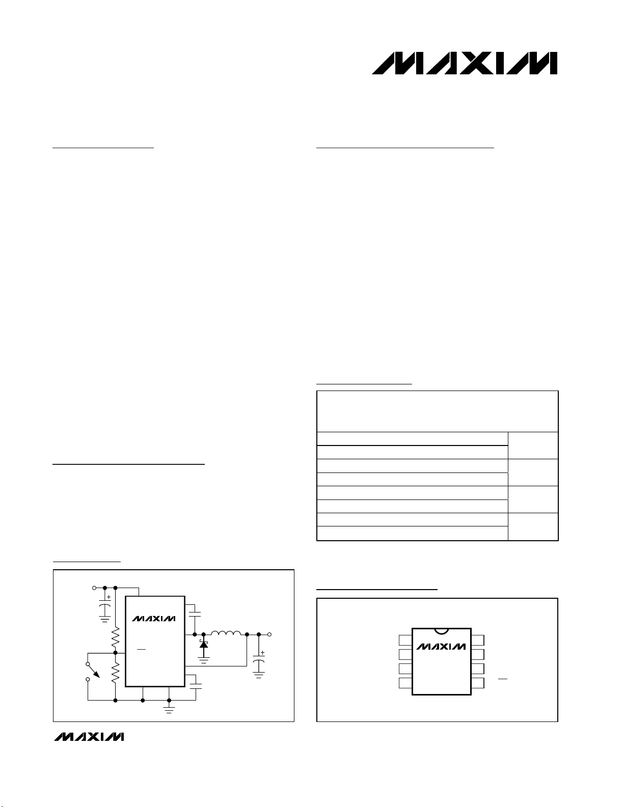
Pin Configuration
MAX5035
GND
BST
LX
V
IN
SGND
FB
D1
50SQ100
VD
100µH
V
OUT
5V
V
IN
7.5V TO 76V
68µF
0.1µF
0.1µF
68µF
ON
OFF
R1
R2
ON/OFF
Typical Operating Circuit
PART TEMP RANGE
MAX5035AUSA 0°C to +85°C 8 SO
MAX5035AUPA 0°C to +85°C 8 PDIP
MAX5035BUSA 0°C to +85°C 8 SO
MAX5035BUPA 0°C to +85°C 8 PDIP
MAX5035CUSA 0°C to +85°C 8 SO
MAX5035CUPA 0°C to +85°C 8 PDIP
MAX5035DUSA 0°C to +85°C 8 SO
MAX5035DUPA 0°C to +85°C 8 PDIP
PINPACKAGE
OUTPUT
VOLTAGE
(V)
3.3
5.0
12
ADJ
TOP VIEW
1
BST
VD
2
SGND
FB
MAX5035
3
4
SO/PDIP
8
7
6
5
LX
V
IN
GND
ON/OFF
Page 2
MAX5035
1A, 76V, High-Efficiency MAXPower
Step-Down DC-DC Converter
2 _______________________________________________________________________________________
ABSOLUTE MAXIMUM RATINGS
Stresses beyond those listed under “Absolute Maximum Ratings” may cause permanent damage to the device. These are stress ratings only, and functional
operation of the device at these or any other conditions beyond those indicated in the operational sections of the specifications is not implied. Exposure to
absolute maximum rating conditions for extended periods may affect device reliability.
(Voltages referenced to GND, unless otherwise specified.)
V
IN
.........................................................................-0.3V to +80V
SGND ....................................................................-0.3V to +0.3V
LX.................................................................-0.8V to (V
IN
+ 0.3V)
BST ...............................................................-0.3V to (V
IN
+ 10V)
BST (transient < 100ns)................................-0.3V to (V
IN
+ 15V)
BST to LX................................................................-0.3V to +10V
BST to LX (transient < 100ns) ................................-0.3V to +15V
ON/OFF........................................................-0.3V to (V
IN
+ 0.3V)
VD...........................................................................-0.3V to +12V
FB
MAX5035A/MAX5035B/MAX5035C ...................-0.3V to +15V
MAX5035D .........................................................-0.3V to +12V
V
OUT
Short-Circuit Duration...........................................Indefinite
VD Short-Circuit Duration ..............................................Indefinite
Continuous Power Dissipation (T
A
= +70°C)
8-Pin PDIP (derate 9.1mW/°C above +70°C)...............727mW
8-Pin SO (derate 5.9mW/°C above +70°C)..................471mW
Operating Temperature Range
MAX5035_U_ _ ...................................................0°C to +85°C
Storage Temperature Range .............................-65°C to +150°C
Junction Temperature......................................................+150°C
Lead Temperature (soldering, 10s) .................................+300°C
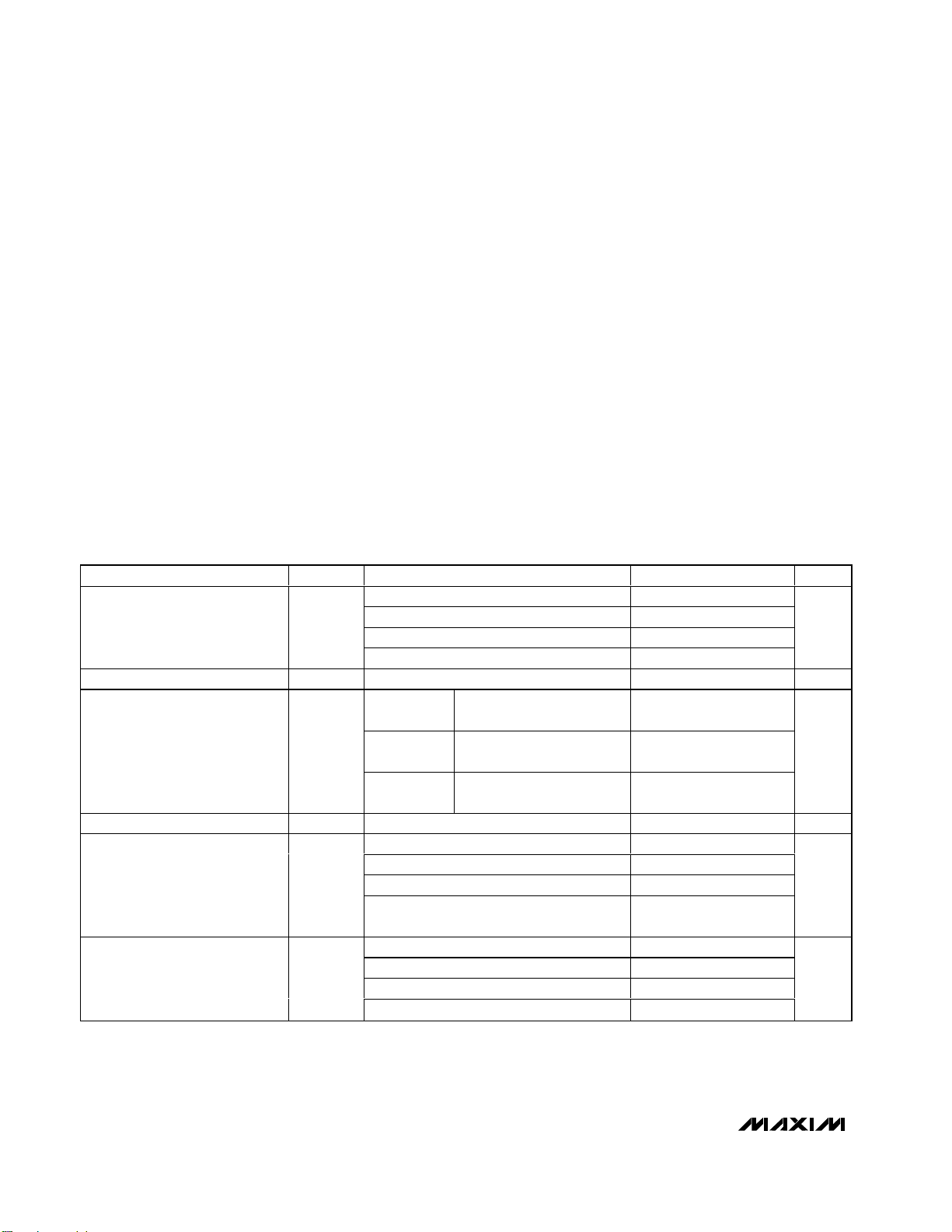
ELECTRICAL CHARACTERISTICS
(VIN= +12V, V
ON/OFF
= +12V, I
OUT
= 0, TA= 0°C to +85°C, unless otherwise noted. Typical values are at TA= +25°C. See the
Typical Application Circuit.)
Input Voltage Range V
Undervoltage Lockout UVLO 5.2 V
Output Voltage V
Feedback Voltage V
Quiescent Supply Current I
PARAMETER SYMBOL CONDITIONS MIN TYP MAX UNITS
MAX5035A 7.5 76.0
MAX5035B 7.5 76.0
IN
MAX5035C 15 76
MAX5035D 7.5 76.0
V
IN
I
OUT
V
IN
I
OUT
V
IN
I
OUT
= 0.5A, MAX5035A 86
LOAD
= 0.5A, MAX5035B 90
LOAD
= 0.5A, MAX5035C 94Efficiency η
LOAD
= 5V, I
OUT
OUT
FB
Q
MAX5035A
MAX5035B
MAX5035C
VIN = 7.5V to 76V, MAX5035D 1.192 1.221 1.250 V
VIN = 12V, I
VIN = 12V, I
VIN = 24V, I
V
= 12V, V
IN
MAX5035D
VFB = 3.5V, VIN = 7.5V to 76V, MAX5035A 350 460
VFB = 5.5V, VIN = 7.5V to 76V, MAX5035B 350 460
VFB = 13V, VIN = 15V to 76V, MAX5035C 350 460
VFB = 1.3V, MAX5035D 350 460
= 7.5V to 76V,
= 20mA to 1A
= 7.5V to 76V,
= 20mA to 1A
= 15V to 76V,
= 20mA to 1A
= 0.5A,
LOAD
3.185 3.3 3.415
4.85 5.0 5.15
11.64 12 12.36
90
V
V
%
µA
Page 3
MAX5035
1A, 76V, High-Efficiency MAXPower
Step-Down DC-DC Converter
_______________________________________________________________________________________ 3
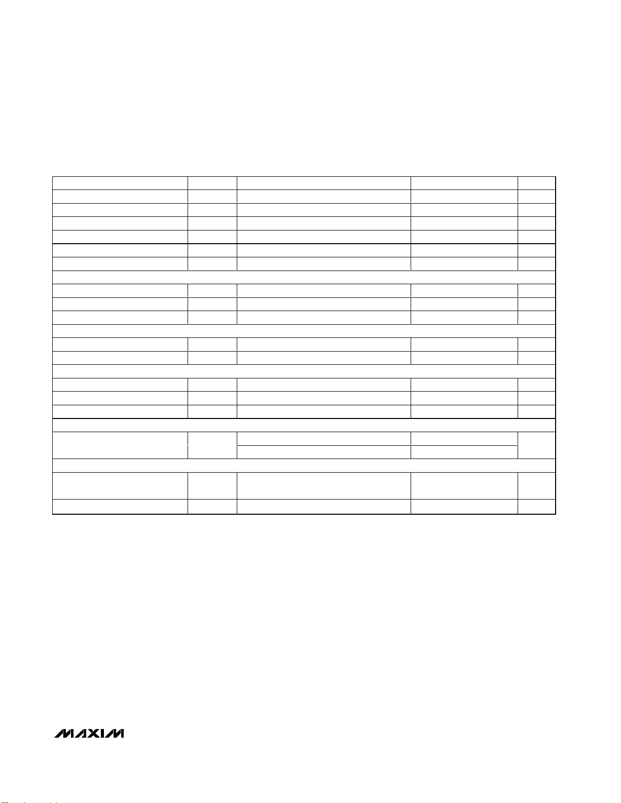
ELECTRICAL CHARACTERISTICS (continued)
(VIN= +12V, V
ON/OFF
= +12V, I
OUT
= 0, TA= 0°C to +85°C, unless otherwise noted. Typical values are at TA= +25°C. See the
Typical Application Circuit.)
)
Note 1: Switch current at which current limit is activated.
Shutdown Current I
Peak Switch Current Limit I
Switch Leakage Current I
Switch On-Resistance R
PFM Threshold I
FB Input Bias Current I
ON/OFF CONTROL INPUT
ON/OFF Input-Voltage Threshold V
ON/OFF Input-Voltage Hysteresis V
ON/OFF Input Current I
OSCILLATOR
Oscillator Frequency f
Maximum Duty Cycle D
VOLTAGE REGULATOR
Regulator Output Voltage VD VIN = 8.5V to 76V, IL = 0mA 6.9 7.8 8.8 V
Dropout Voltage 7.5V ≤ VIN ≤ 8.5V, IL = 1mA 2.0 V
Load Regulation ∆VD/∆IVD0 to 5mA 150 mV/mA
PACKAGE THERMAL CHARACTERISTICS
Thermal Resistance
(Junction to Ambient)
THERMAL SHUTDOWN
Thermal-Shutdown Junction
Temperature
Thermal-Shutdown Hysteresis T
PARAMETER SYMBOL CONDITIONS MIN TYP MAX UNITS
SHDN
LIM
OL
DS(ON
PFM
ON/OFF
HYST
ON/OFFVON/OFF
OSC
MAX
θ
JA
T
SH
HYST
V
(Note 1) 1.80 2.40 A
VIN = 76V, V
I
Minimum switch current in any cycle 55 85 110 mA
MAX5035D -12 +0.01 +12 nA
B
Rising trip point 1.53 1.69 1.85 V
MAX5035D 95 %
SO package (JEDEC 51) 170
DIP package (JEDEC 51) 110
= 0V, VIN = 7.5V to 76V 10 45 µA
ON/OFF
= 0V, VLX = 0V 1 µA
ON/OFF
= 1A 0.40 0.80 Ω
SWITCH
100 mV
= 0V to V
IN
109 125 135 kHz
10 150 nA
+160 °C
20 °C
°C/W
Page 4
MAX5035
1A, 76V, High-Efficiency MAXPower
Step-Down DC-DC Converter
4 _______________________________________________________________________________________
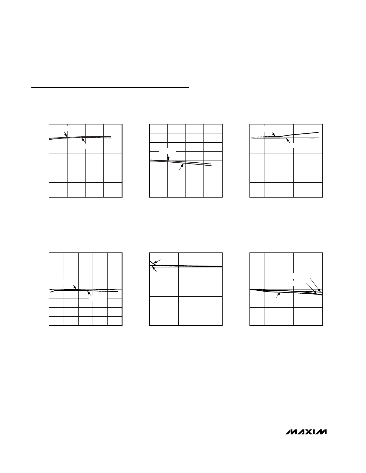
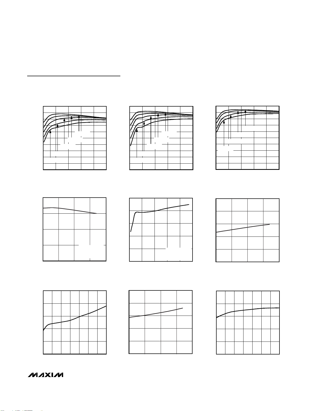
Typical Operating Characteristics
(VIN= 12V, V
ON/OFF
= 12V, TA= 0°C to +85°C, unless otherwise noted. Typical values are at TA= +25°C. See the Typical Application
Circuit, if applicable.)
OUTPUT VOLTAGE vs. TEMPERATURE
(MAX5035AUSA, V
3.40
I
= 0.1A
OUT
3.36
3.32
(V)
OUT
V
3.28
3.24
3.20
0 100
OUTPUT VOLTAGE vs. TEMPERATURE
OUT
I
= 1A
OUT
5025
TEMPERATURE (°C)
= 3.3V)
75
MAX5035 toc01
5.20
(MAX5035DUSA, V
5.15
5.10
I
= 0.1A
OUT
I
= 1A
OUT
0 100
25 50
TEMPERATURE (°C)
(V)
V
OUT
5.05
5.00
4.95
4.90
4.85
4.80
OUT
= 5V)
MAX5035 toc02
75
LINE REGULATION
I
OUT
OUT
= 1A
= 3.3V)
MAX5035 toc03
65503520
3.40
(MAX5035AUSA, V
I
= 0.1A
OUT
3.36
3.32
3.28
OUTPUT VOLTAGE (V)
3.24
3.20
580
INPUT VOLTAGE (V)
LINE REGULATION
5.20
(MAX5035DUSA, V
5.15
5.10
5.05
I
= 0.1A
OUT
5.00
4.95
OUTPUT VOLTAGE (V)
4.90
4.85
4.80
580
INPUT VOLTAGE (V)
= 5V)
OUT
MAX5035 toc04
(V)
OUT
I
= 1A
OUT
655020 35
V
(MAX5035AUSA, V
3.40
VIN = 76V
3.36
VIN = 7.5V, 24V
3.32
3.28
3.24
3.20
0 1000
LOAD REGULATION
OUT
I
(mA)
LOAD
= 3.3V)
800600400200
MAX5035 toc05
LOAD REGULATION
5.10
(MAX5035DUSA, V
5.05
(V)
5.00
OUT
V
VIN = 76V
4.95
4.90
0 1000
I
LOAD
OUT
VIN = 24V
VIN = 7.5V
(mA)
= 5V)
MAX5035 toc06
800600400200
Page 5
MAX5035
1A, 76V, High-Efficiency MAXPower
Step-Down DC-DC Converter
_______________________________________________________________________________________ 5
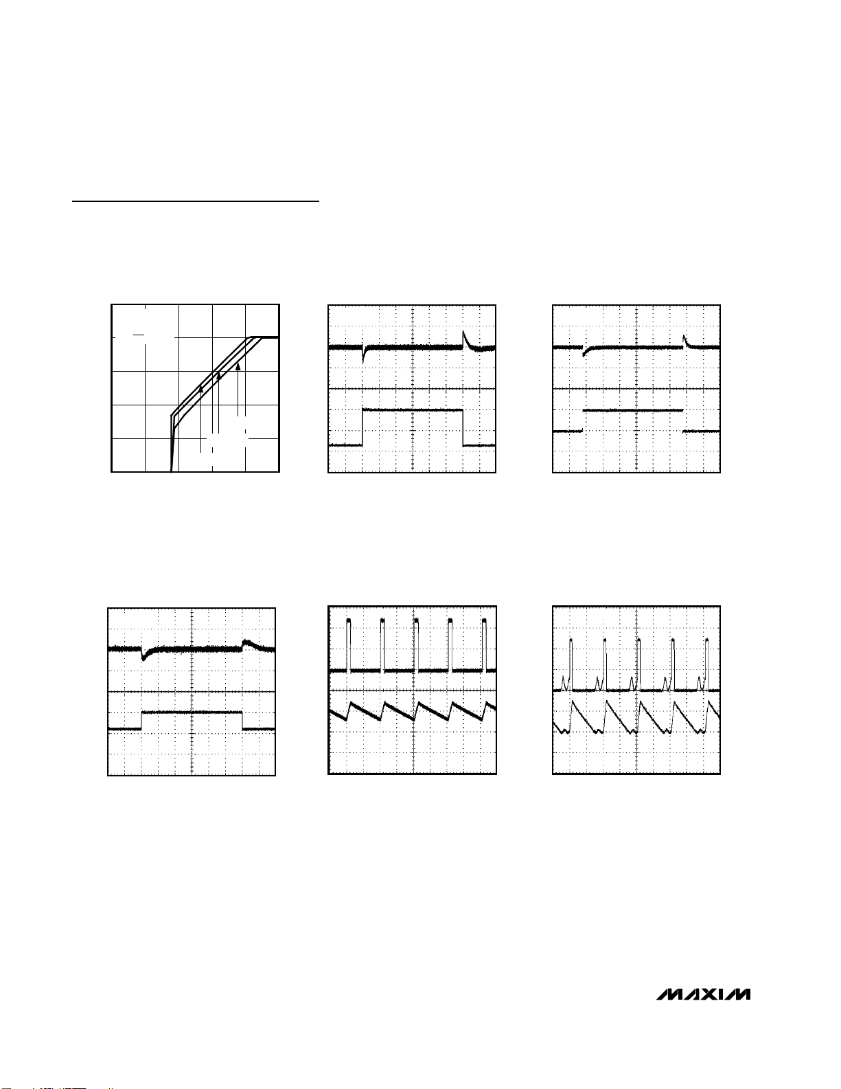
Typical Operating Characteristics (continued)
(VIN= 12V, V
ON/OFF
= 12V, TA= 0°C to +85°C, unless otherwise noted. Typical values are at TA= +25°C. See the Typical Application
Circuit, if applicable.)
EFFICIENCY vs. LOAD CURRENT
(MAX5035AUSA, V
100
90
80
70
60
50
40
EFFICIENCY (%)
30
20
10
VIN = 48V
VIN = 76V
0
0 1000
VIN = 12V
VIN = 24V
LOAD CURRENT (mA)
OUTPUT CURRENT LIMIT
vs. TEMPERATURE
2.0
1.5
1.0
0.5
OUTPUT CURRENT LIMIT (A)
0
0 100
5025
TEMPERATURE (°C)
= 3.3V)
OUT
VIN = 7.5V
MAX5035DUSA
= 5V
V
OUT
5% DROP IN V
EFFICIENCY vs. LOAD CURRENT
100
(MAX5035DUSA, V
90
MAX5035 toc07
80
70
60
50
40
EFFICIENCY (%)
30
20
10
800600400200
VIN = 48V
VIN = 76V
0
0 1000
VIN = 12V
VIN = 24V
LOAD CURRENT (mA)
OUT
VIN = 7.5V
= 5V)
MAX5035 toc08
EFFICIENCY (%)
800600400200
OUTPUT CURRENT LIMIT
vs. INPUT VOLTAGE
2.0
MAX5035 toc10
1.7
1.4
1.1
OUTPUT CURRENT LIMIT (A)
0.8
OUT
75
0.5
580
INPUT VOLTAGE (V)
MAX5035DUSA
V
5% DROP IN VOUT
65503520
OUT
= 5V
MAX5035 toc11
QUIESCENT SUPPLY CURRENT (µA)
EFFICIENCY vs. LOAD CURRENT
(MAX5035DUSA, V
100
90
80
70
60
50
40
VIN = 76V
30
20
10
0
0 1000
VIN = 15V
VIN = 24V
VIN = 48V
LOAD CURRENT (mA)
OUT
= 12V)
QUIESCENT SUPPLY CURRENT
vs. TEMPERATURE
350
320
290
260
230
200
0 100
25
TEMPERATURE (°C)
7550
MAX5035 toc09
800600400200
MAX5035 toc12
QUIESCENT SUPPLY CURRENT
SHUTDOWN CURRENT
vs. INPUT VOLTAGE
MAX5035 toc13
20
16
12
8
SHUTDOWN CURRENT (µA)
4
0
0 100
350
320
290
260
230
QUIESCENT SUPPLY CURRENT (µA)
200
676
INPUT VOLTAGE (V)
665646362616
vs. TEMPERATURE
TEMPERATURE (°C)
SHUTDOWN CURRENT vs. INPUT VOLTAGE
20
MAX5035 toc14
16
12
8
SHUTDOWN CURRENT (µA)
4
755025
0
676
INPUT VOLTAGE (V)
MAX5035 toc15
665646362616
Page 6
MAX5035
1A, 76V, High-Efficiency MAXPower
Step-Down DC-DC Converter
6 _______________________________________________________________________________________
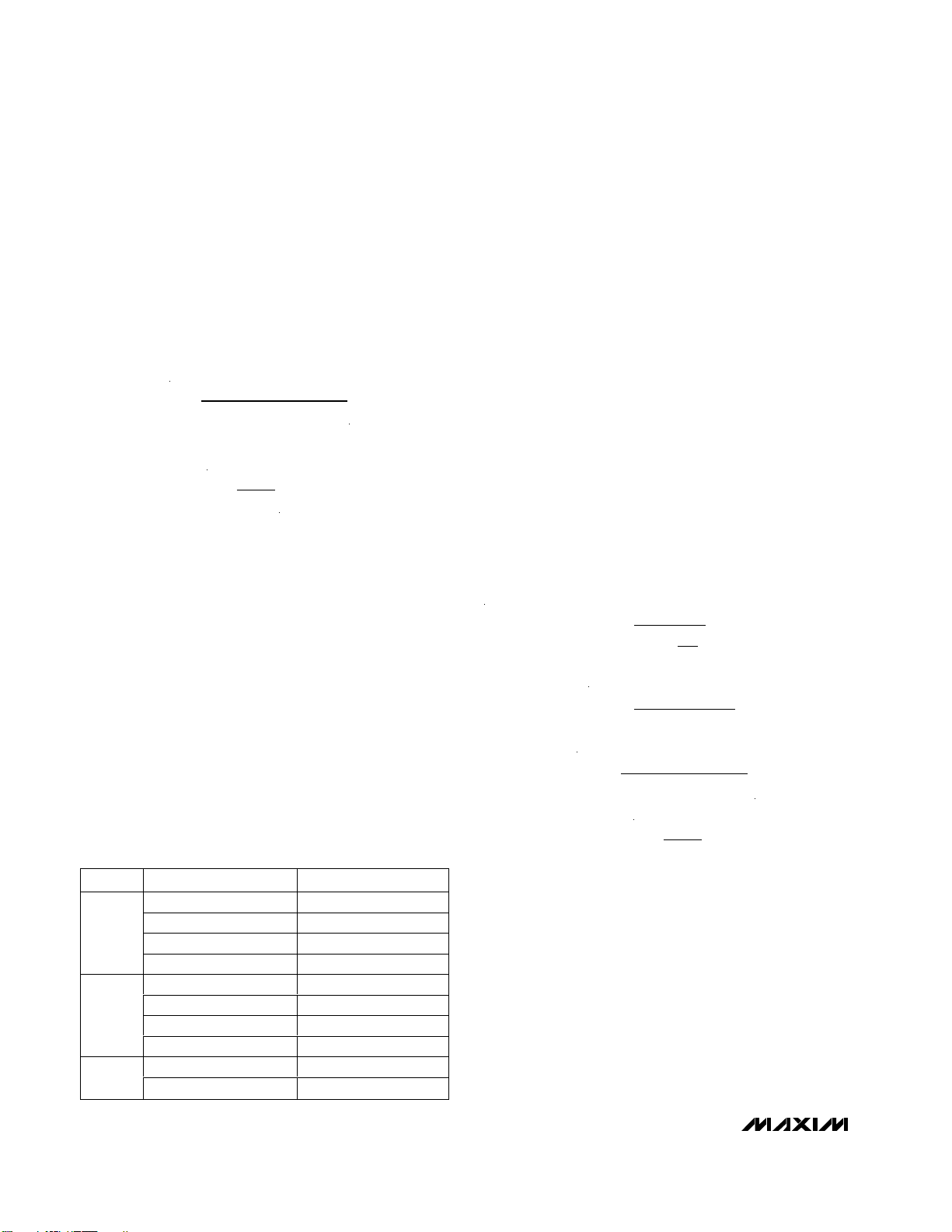
Typical Operating Characteristics (continued)
(VIN= 12V, V
ON/OFF
= 12V, TA= 0°C to +85°C, unless otherwise noted. Typical values are at TA= +25°C. See the Typical Application
Circuit, if applicable.)
MAX5035DUSA
LOAD-TRANSIENT RESPONSE
MAX5035 toc19
400µs/div
B
A
A: V
OUT
, 200mV/div, AC-COUPLED
B: V
OUT
, 500mA/div, 0.1A TO 0.5A
V
OUT
= 5V
MAX5035DUSA LX WAVEFORMS
MAX5035 toc20
4µs/div
B
0
A
0
A: SWITCH VOLTAGE (LX PIN), 20V/div, (VIN = 48V)
B: INDUCTOR CURRENT, 500mA/div (I
OUT
= 1A)
MAX5035DUSA LX WAVEFORMS
MAX5035 toc21
4µs/div
B
0
A
0
A: SWITCH VOLTAGE (LX PIN), 20V/div, (VIN = 48V)
B: INDUCTOR CURRENT, 200mA/div (I
OUT
= 100mA)
OUTPUT VOLTAGE
vs. INPUT VOLTAGE
15
MAX5035DUSA
= 12V
V
OUT
= V
V
12
ON/OFF
IN
9
(V)
OUT
V
6
3
0
015
I
OUT
VIN (V)
= 0
MAX5035DUSA
LOAD-TRANSIENT RESPONSE
V
= 5V
OUT
MAX5035 toc16
I
= 1A
OUT
I
= 0.3A
OUT
12963
, 200mV/div, AC-COUPLED
A: V
OUT
, 500mA/div, 0.1A TO 1A
B: I
OUT
400µs/div
MAX5035 toc17
V
A
B
A: V
B: V
MAX5035DUSA
LOAD-TRANSIENT RESPONSE
= 5V
OUT
400µs/div
, 200mV/div, AC-COUPLED
OUT
, 500mA/div, 0.5A TO 1A
OUT
MAX5035 toc18
A
B
Page 7

MAX5035
1A, 76V, High-Efficiency MAXPower
Step-Down DC-DC Converter
_______________________________________________________________________________________ 7
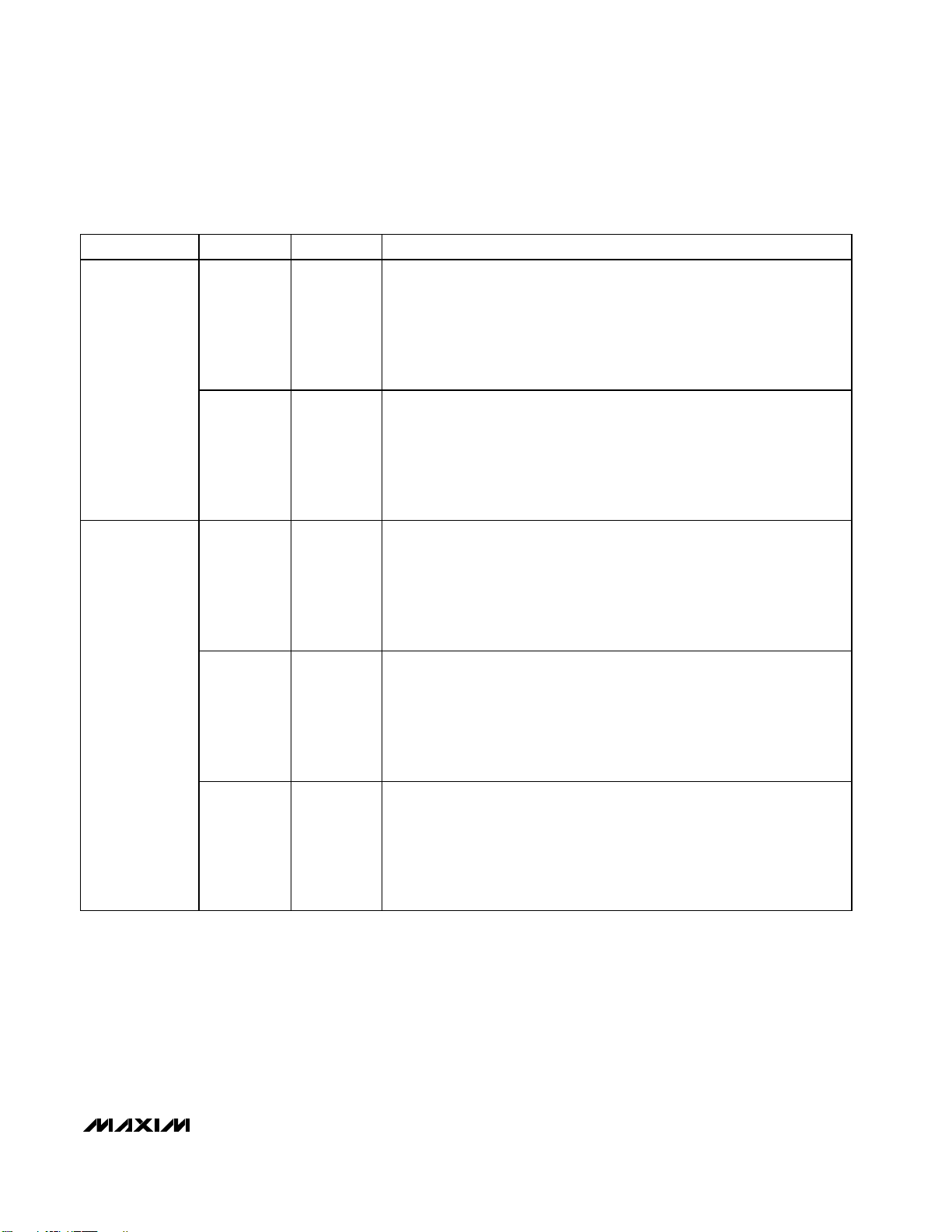
Typical Operating Characteristics (continued)
(VIN= 12V, V
ON/OFF
= 12V, TA= 0°C to +85°C, unless otherwise noted. Typical values are at TA= +25°C. See the Typical Application
Circuit, if applicable.)
A: SWITCH VOLTAGE (LX PIN), 20V/div, VIN = 48V
B: INDUCTOR CURRENT, 200mA/div (I
MAX5035DUSA LX WAVEFORMS
4µs/div
MAX5035 toc22
= 0)
OUT
MAX5035DUSA STARTUP WAVEFORM
= 1A)
(I
O
MAX5035 toc24
MAX5035DUSA STARTUP WAVEFORM
A
0
B
0
0
0
A: V
, 2V/div
ON/OFF
, 2V/div
B: V
OUT
PEAK SWITCH CURRENT
3.0
A
2.5
= 0)
(I
O
1ms/div
vs. INPUT VOLTAGE
MAX5035 toc23
A
B
MAX5035 toc25
2.0
0
0
1ms/div
A: V
, 2V/div
ON/OFF
, 2V/div
B: V
OUT
B
1.5
PEAK SWITCH CURRENT (A)
1.0
0.5
676
INPUT VOLTAGE (V)
MAX5035DUSA
= 5V
V
OUT
5% DROP IN V
56 6646362616
OUT
Page 8

MAX5035
1A, 76V, High-Efficiency MAXPower
Step-Down DC-DC Converter
8 _______________________________________________________________________________________
Pin Description
Block Diagram
PIN NAME FUNCTION
1 BST Boost Capacitor Connection. Connect a 0.1µF ceramic capacitor from BST to LX.
2 VD Internal Regulator Output. Bypass VD to GND with a 0.1µF ceramic capacitor.
3 SGND Internal Connection. SGND must be connected to GND.
4FB
5 ON/OFF
6 GND Ground
7VINInput Voltage. Bypass VIN to GND with a low ESR capacitor as close to the device as possible.
8 LX Source Connection of Internal High-Side Switch
ON/OFF
1.69V
VD
Output Sense Feedback Connection. For fixed output voltage (MAX5035A, MAX5035B, MAX5035C),
connect FB to V
set V
. VFB regulating set point is 1.22V.
OUT
. For adjustable output voltage (MAX5035D), use an external resistive voltage-divider to
OUT
Shutdown Control Input. Pull ON/OFF low to put the device in shutdown mode. Drive ON/OFF high for
normal operation.
ENABLE
REGULATOR
(FOR DRIVER)
REGULATOR
(FOR ANALOG)
V
REF
OSC
RAMP
CPFM
CILIM
I
REF-PFM
I
REF-LIM
HIGH-SIDE
CURRENT
SENSE
V
IN
MAX5035
CLK
CONTROL
LOGIC
THERMAL
SHUTDOWN
SGND
GND
FB
R
h
x1
R
l
TYPE 3
COMPENSATION
V
REF
EAMP
RAMP
CPWM
BST
LX
Page 9

MAX5035
1A, 76V, High-Efficiency MAXPower
Step-Down DC-DC Converter
_______________________________________________________________________________________ 9
Detailed Description
The MAX5035 step-down DC-DC converter operates
from a 7.5V to 76V input voltage range. A unique voltage-mode control scheme with voltage feedforward
and an internal switching DMOS FET provides high efficiency over a wide input voltage range. This pulsewidth modulated converter operates at a fixed 125kHz
switching frequency. The device also features automatic pulse-skipping mode to provide low quiescent current and high efficiency at light loads. Under no load,
the MAX5035 consumes only 350µA, and in shutdown
mode, consumes only 10µA. The MAX5035 also features undervoltage lockout, hiccup mode output shortcircuit protection, and thermal shutdown.
Shutdown Mode
Drive ON/OFF to ground to shut down the MAX5035.
Shutdown forces the internal power MOSFET off, turns
off all internal circuitry, and reduces the VINsupply current to 10µA (typ). The ON/OFF rising threshold is
1.69V (typ). Before any operation begins, the voltage at
ON/OFF must exceed 1.69V (typ). The ON/OFF input
has 100mV hysteresis.
Undervoltage Lockout (UVLO)
Use the ON/OFF function to program the UVLO threshold at the input. Connect a resistive voltage-divider
from VINto GND with the center node to ON/OFF as
shown in Figure 1. Calculate the threshold value by
using the following formula:
The minimum recommended V
UVLO(TH)
is 6.5V, 7.5V,
and 13V for the output voltages of 3.3V, 5V, and 12V,
respectively. The recommended value for R2 is less
than 1MΩ.
If the external UVLO threshold-setting divider is not
used, an internal undervoltage lockout feature monitors
the supply voltage at VINand allows operation to start
when V
IN
rises above 5.2V (typ). This feature can be
used only when VINrise time is faster than 2ms. For
slower VINrise time, use the resistive-divider at
ON/OFF.
Boost High-Side Gate Drive (BST)
Connect a flying bootstrap capacitor between LX and
BST to provide the gate-drive voltage to the high-side
N-channel DMOS switch. The capacitor is alternately
charged from the internally regulated output voltage VD
and placed across the high-side DMOS driver. Use a
0.1µF, 16V ceramic capacitor located as close to the
device as possible.
On startup, an internal low-side switch connects LX to
ground and charges the BST capacitor to VD. Once the
BST capacitor is charged, the internal low-side switch
is turned off and the BST capacitor voltage provides
the necessary enhancement voltage to turn on the
high-side switch.
Thermal Overload Protection
The MAX5035 features integrated thermal overload protection. Thermal overload protection limits total power
dissipation in the device, and protects the device in the
event of a fault condition. When the die temperature
exceeds +160°C, an internal thermal sensor signals the
shutdown logic, turning off the internal power MOSFET
and allowing the IC to cool. The thermal sensor turns the
internal power MOSFET back on after the IC’s die temperature cools down to +140°C, resulting in a pulsed
output under continuous thermal overload conditions.
Applications Information
Setting the Output Voltage
The MAX5035A/B/C have preset output voltages of 3.3V,
5.0V, and 12V, respectively. Connect FB to the preset
output voltage (see the Typical Operating Circuit).
The MAX5035D offers an adjustable output voltage. Set
the output voltage with a resistive voltage-divider connected from the circuit’s output to ground (Figure 1).
Connect the center node of the divider to FB. Choose
R4 less than 15kΩ, then calculate R3 as follows:
R
V
R
OUT
3
122
122
4=
−
×
(.)
.
Figure 1. Adjustable Output Voltage
V
UVLO TH()
1
R
×1
.=+
185
2
R
V
V
IN
7.5V TO 76V
68µF
V
R1
R2
IN
ON/OFF
MAX5035D
SGND
GND
LX
BST
FB
VD
0.1µF
0.1µF
100µH
D1
50SQ100
41.2kΩ
13.3kΩ
V
OUT
5V
C
OUT
68µF
R3
R4
Page 10
MAX5035
1A, 76V, High-Efficiency MAXPower
Step-Down DC-DC Converter
10 ______________________________________________________________________________________
The MAX5035 features internal compensation for optimum closed-loop bandwidth and phase margin. With
the preset compensation, it is strongly advised to sense
the output immediately after the primary LC.
Inductor Selection
The choice of an inductor is guided by the voltage difference between VINand V
OUT
, the required output
current, and the operating frequency of the circuit. Use
an inductor with a minimum value given by:
where:
I
OUTMAX
is the maximum output current required, and
fSWis the operating frequency of 125kHz. Use an inductor with a maximum saturation current rating equal to at
least twice the peak output current of the circuit. Use
inductors with low DC resistance for higher efficiency.
Selecting a Rectifier
The MAX5035 requires an external Schottky rectifier as
a freewheeling diode. Connect this rectifier close to the
device using short leads and short PC board traces.
Choose a rectifier with a continuous current rating
greater than the highest expected output current. Use a
rectifier with a voltage rating greater than the maximum
expected input voltage, V
IN
. Use a low forward-voltage
Schottky rectifier for proper operation and high efficiency. Avoid higher than necessary reverse-voltage
Schottky rectifiers that have higher forward-voltage
drops. Use a Schottky rectifier with forward-voltage
drop (V
FB
) less than 0.45V at +25°C and maximum load
current to avoid forward biasing of the internal body
diode (LX to ground). Internal body diode conduction
may cause excessive junction temperature rise and
thermal shutdown. Use Table 1 to choose the proper
rectifier at different input voltages and output current.
Input Bypass Capacitor
The discontinuous input current waveform of the buck
converter causes large ripple currents in the input
capacitor. The switching frequency, peak inductor current, and the allowable peak-to-peak voltage ripple that
reflects back to the source dictate the capacitance
requirement. The MAX5035 high switching frequency
allows the use of smaller value input capacitors.
The input ripple is comprised of ∆VQ(caused by the
capacitor discharge) and ∆V
ESR
(caused by the ESR of
the capacitor). Use low-ESR aluminum electrolytic
capacitors with high ripple-current capability at the input.
Assuming that the contribution from the ESR and capacitor discharge is equal to 90% and 10%, respectively, calculate the input capacitance and the ESR required for a
specified ripple using the following equations:
I
OUT
is the maximum output current of the converter
and fSWis the oscillator switching frequency (125kHz).
For example, at VIN= 48V, V
OUT
= 3.3V, the ESR and
input capacitance are calculated for the input peak-topeak ripple of 100mV or less yielding an ESR and
capacitance value of 80mΩ and 51µF, respectively.
Low-ESR, ceramic, multilayer chip capacitors are recommended for size-optimized application. For ceramic
capacitors, assume the contribution from ESR and capacitor discharge is equal to 10% and 90%, respectively.
The input capacitor must handle the RMS ripple current
without significant rise in temperature. The maximum
capacitor RMS current occurs at about 50% duty cycle.
D
V
V
OUT
IN
=
∆I
VV V
Vf L
L
IN OUT OUT
IN SW
=
−×
××
()
,
C
IDD
Vf
IN
OUT
QSW
=
×−
×
()1
∆
ESR
V
I
I
IN
ESR
OUT
L
=
+
∆
∆
2
D
V
V
OUT
IN
=
L
VV D
If
IN OUT
OUTMAX SW
=
−×
××
()
.02
Table 1. Diode Selection
where
V
IN
7.5 to 36
7.5 to 56
7.5 to 76
(V) DIODE PART NUMBER MANUFACTURER
15MQ040N IR
B240A Diodes, Inc.
B240 Central Semiconductor
MBRS240, MBRS1540 ON Semiconductor
30BQ060 IR
B360A Diodes, Inc.
CMSH3-60 Central Semiconductor
MBRD360, MBR3060 ON Semiconductor
50SQ100, 50SQ80 IR
MBRM5100 Diodes, Inc.
Page 11

MAX5035
1A, 76V, High-Efficiency MAXPower
Step-Down DC-DC Converter
______________________________________________________________________________________ 11
Ensure that the ripple specification of the input capacitor exceeds the worst-case capacitor RMS ripple current. Use the following equations to calculate the input
capacitor RMS current:
I
PRMS
is the input switch RMS current, I
AVGin
is the
input average current, and η is the converter efficiency.
The ESR of aluminum electrolytic capacitors increases
significantly at cold temperatures. Use a 1µF or greater
value ceramic capacitor in parallel with the aluminum
electrolytic input capacitor, especially for input voltages
below 8V.
Output Filter Capacitor
The worst-case peak-to-peak and RMS capacitor ripple
current, allowable peak-to-peak output ripple voltage,
and the maximum deviation of the output voltage during load steps determine the capacitance and the ESR
requirements for the output capacitors.
The output capacitance and its ESR form a zero, which
improves the closed-loop stability of the buck regulator.
Choose the output capacitor so the ESR zero frequency
(fZ) occurs between 20kHz to 40kHz. Use the following
equation to verify the value of fZ. Capacitors with 100mΩ
to 250mΩ ESR are recommended to ensure the closedloop stability, while keeping the output ripple low.
The output ripple is comprised of ∆VOQ(caused by the
capacitor discharge) and ∆V
OESR
(caused by the ESR
of the capacitor). Use low-ESR tantalum or aluminum
electrolytic capacitors at the output. Assuming that the
contribution from the ESR and capacitor discharge
equal 80% and 20% respectively, calculate the output
capacitance and the ESR required for a specified ripple using the following equations:
The MAX5035 has an internal soft-start time (tSS) of
400µs. It is important to keep the output rise time at
startup below tSSto avoid output overshoot. The output
rise time is directly proportional to the output capacitor.
Use 68µF or lower capacitance at the output to control
the overshoot below 5%.
In a dynamic load application, the allowable deviation
of the output voltage during the fast-transient load dictates the output capacitance value and the ESR. The
output capacitors supply the step load current until the
controller responds with a greater duty cycle. The
response time (t
RESPONSE
) depends on the closedloop bandwidth of the converter. The resistive drop
across the capacitor ESR and capacitor discharge
cause a voltage droop during a step load. Use a combination of low-ESR tantalum and ceramic capacitors
for better transient load and ripple/noise performance.
Keep the maximum output voltage deviation above the
tolerable limits of the electronics being powered.
Assuming a 50% contribution each from the output
capacitance discharge and the ESR drop, use the following equations to calculate the required ESR and
capacitance value:
where I
STEP
is the load step and t
RESPONSE
is the
response time of the controller. Controller response
time is approximately one-third of the reciprocal of the
closed-loop unity-gain bandwidth, 20kHz typically.
PC Board Layout Considerations
Proper PC board layout is essential. Minimize ground
noise by connecting the anode of the Schottky rectifier,
the input bypass capacitor ground lead, and the output
filter capacitor ground lead to a single point (“star”
C
It
V
OUT
STEP RESPONSE
OQ
=
×
∆
ESR
V
I
OUT
OESR
STEP
=
∆
C
I
Vf
OUT
L
OQ SW
≈
××
∆
∆22.
ESR
V
I
OUT
OESR
L
=
∆
∆
f
C ESR
Z
OUT OUT
=
×× ×
1
2 π
IIIII
D
I
VI
V
II
I
II
I
and D
V
V
PRMS PK DC PK DC
AVGIN
OUT OUT
IN
PK OUT
L
DC OUT
L
OUT
IN
=++×
()
×
=
×
×
=+ = −
=
22
3
22
,
η
∆∆
III
where
CRMS PRMS AVGIN
=−
22
Page 12

MAX5035
1A, 76V, High-Efficiency MAXPower
Step-Down DC-DC Converter
12 ______________________________________________________________________________________
ground configuration). A ground plane is required.
Minimize lead lengths to reduce stray capacitance,
trace resistance, and radiated noise. In particular,
place the Schottky rectifier diode right next to the
device. Also, place BST and VD bypass capacitors
very close to the device. Use the PC board copper
plane connecting to VINand LX for heat sinking.
Figure 2. Fixed Output Voltages
Table 2. Typical External Components Selection (Circuit of Figure 2)
Application Circuits
V
IN
R1
R2
VIN (V) V
7.5 to 76 3.3 0.5
7.5 to 76 3.3 1
7.5 to 76 5 0.5
7.5 to 76 5 1
OUT
(V) I
C
IN
V
IN
MAX5035
ON/OFF
SGND
(A) EXTERNAL COMPONENTS
OUT
BST
LX
FB
VD
GND
= 68µF, Panasonic, EEVFK2A680Q
C
IN
C
= 68µF, Vishay Sprague, 594D686X_010C2T
OUT
= 0.1µF, 0805
C
BST
0.1µF
0.1µF
L1
D1
R1 = 1MΩ ±1%, 0805
R2 = 384kΩ ±1%, 0805
D1 = 50SQ100, IR
L1 = 100µH, Coilcraft Inc., DO5022P-104
C
= 68µF, Panasonic, EEVFK2A680Q
IN
= 68µF, Vishay Sprague, 594D68X_010C2T
C
OUT
C
= 0.1µF, 0805
BST
R1 = 1MΩ ±1%, 0805
R2 = 384kΩ ±1%, 0805
D1 = 50SQ100, IR
L1 = 100µH, Coilcraft Inc., DO5022P-104
V
OUT
C
OUT
C
= 68µF, Panasonic, EEVFK2A680Q
IN
= 15µF, Vishay Sprague, 594D156X0025C2T
C
OUT
C
= 0.1µF, 0805
BST
15 to 76 12 1
R1 = 1MΩ ±1%, 0805
R2 = 139kΩ ±1%, 0805
D1 = 50SQ100, IR
L1 = 220µH, Coilcraft Inc., DO5022P-224
Page 13
MAX5035
1A, 76V, High-Efficiency MAXPower
Step-Down DC-DC Converter
______________________________________________________________________________________ 13
Table 2. Typical External Components Selection (Circuit of Figure 2) (continued)
VIN (V) V
9 to 14
18 to 36
(V) I
OUT
3.3 1
51
3.3 1
51
(A) EXTERNAL COMPONENTS
OUT
= 220µF, Panasonic, EEVFK1E221P
C
IN
C
= 68µF, Vishay Sprague, 594D686X_010C2T
OUT
= 0.1µF, 0805
C
BST
R1 = 1MΩ ±1%, 0805
R2 = 274kΩ ±1%, 0805
D1 = B220, Diodes Inc.
L1 = 100µH, Coilcraft Inc., DO5022P-104
= 220µF, Panasonic, EEVFK1E221P
C
IN
C
= 68µF, Vishay Sprague, 594D686X_010C2T
OUT
= 0.1µF, 0805
C
BST
R1 = 1MΩ ±1%, 0805
R2 = 274kΩ ±1%, 0805
D1 = B220, Diodes Inc.
L1 = 100µH, Coilcraft Inc., DO5022P-104
C
= 220µF, Panasonic, EEVFK1H221P
IN
= 68µF, Vishay Sprague, 594D686X_010C2T
C
OUT
C
= 0.1µF, 0805
BST
R1 = 1MΩ ±1%, 0805
R2 = 130kΩ ±1%, 0805
D1 = MBRS2040, ON Semiconductor
L1 = 100µH, Coilcraft Inc., DO5022P-104
= 220µF, Panasonic, EEVFK1H221P
C
IN
= 68µF, Vishay Sprague, 594D686X_010C2T
C
OUT
C
= 0.1µF, 0805
BST
R1 = 1MΩ ±1%, 0805
R2 = 130kΩ ±1%, 0805
D1 = MBRS2040, ON Semiconductor
L1 = 100µH, Coilcraft Inc., DO5022P-104
C
= 220µF, Panasonic, EEVFK1H221P
IN
C
= 15µF, Vishay Sprague, 594D156X_0025C2T
OUT
= 0.1µF, 0805
C
BST
12 1
R1 = 1MΩ ±1%, 0805
R2 = 130kΩ ±1%, 0805
D1 = MBRS2040, ON Semiconductor
L1 = 220µH, Coilcraft Inc., DO5022P-224
Page 14

MAX5035
1A, 76V, High-Efficiency MAXPower
Step-Down DC-DC Converter
14 ______________________________________________________________________________________
Table 3. Component Suppliers
Figure 3. Load Temperature Monitoring with ON/
OFF
(Requires Accurate VIN)
SUPPLIER PHONE FAX WEBSITE
AVX 843-946-0238 843-626-3123 www.avxcorp.com
Coilcraft 847-639-6400 847-639-1469 www.coilcraft.com
Diodes Incorporated 805-446-4800 805-446-4850 www.diodes.com
Panasonic 714-373-7366 714-737-7323 www.panasonic.com
Sanyo 619-661-6835 619-661-1055 www.sanyo.com
TDK 847-803-6100 847-390-4405 www.component.tdk.com
Vishay 402-563-6866 402-563-6296 www.vishay.com
MAX5035
PTC*
V
IN
12V
C
IN
68µF
*LOCATE PTC AS CLOSE TO HEAT-DISSIPATING COMPONENTS AS POSSIBLE.
Ct
ON/OFF
V
IN
Rt
SGND
GND
FB
BST
LX
VD
0.1µF
0.1µF
D1
B240
L1
100µH
V
OUT
5V AT 1A
C
OUT
68µF
Page 15

MAX5035
1A, 76V, High-Efficiency MAXPower
Step-Down DC-DC Converter
______________________________________________________________________________________ 15
Figure 4. Dual-Sequenced DC-DC Converters (Startup Delay Determined by R1/R1’, Ct/Ct’ and Rt/Rt’)
Chip Information
TRANSISTOR COUNT: 4344
PROCESS: BiCMOS
GND
GND
FB
BST
LX
VD
0.1µF
FB
BST
LX
VD
0.1µF
0.1µF
0.1µF
L1
220µH
D1
B240
L1'
100µH
D1'
B240
V
7.5V TO 36V
MAX5035B
R1
IN
C
68µF
IN
Ct
ON/OFF
V
IN
Rt
SGND
MAX5035A
C'
68µF
R1'
IN
Ct'
ON/OFF
V
IN
Rt'
SGND
V
V'
3.3V
OUT
5V
OUT
C
OUT
68µF
C'
OUT
68µF
Page 16

MAX5035
1A, 76V, High-Efficiency MAXPower
Step-Down DC-DC Converter
16 ______________________________________________________________________________________
Package Information
(The package drawing(s) in this data sheet may not reflect the most current specifications. For the latest package outline information,
go to www.maxim-ic.com/packages
.)
N
1
e
FRONT VIEW
TOP VIEW
D
INCHES
DIM
MIN
0.053A
0.004
A1
0.014
B
0.007
C
e 0.050 BSC 1.27 BSC
0.150
HE
A
B
A1
C
L
E
H 0.2440.228 5.80 6.20
0.016L
VARIATIONS:
INCHES
MINDIM
D
0.189 0.197 AA5.004.80 8
0.337 0.344 AB8.758.55 14
D
0-8
MAX
0.069
0.010
0.019
0.010
0.157
0.050
MAX
0.3940.386D
MILLIMETERS
MAX
MIN
1.35
1.75
0.10
0.25
0.35
0.49
0.19
0.25
3.80 4.00
0.40 1.27
MILLIMETERS
MAX
MIN
9.80 10.00
N MS012
16
AC
SOICN .EPS
SIDE VIEW
PROPRIETARY INFORMATION
TITLE:
PACKAGE OUTLINE, .150" SOIC
REV.DOCUMENT CONTROL NO.APPROVAL
21-0041
1
B
1
Page 17

MAX5035
1A, 76V, High-Efficiency MAXPower
Step-Down DC-DC Converter
Maxim cannot assume responsibility for use of any circuitry other than circuitry entirely embodied in a Maxim product. No circuit patent licenses are
implied. Maxim reserves the right to change the circuitry and specifications without notice at any time.
Maxim Integrated Products, 120 San Gabriel Drive, Sunnyvale, CA 94086 408-737-7600 ____________________ 17
© 2003 Maxim Integrated Products Printed USA is a registered trademark of Maxim Integrated Products.
Package Information (continued)
(The package drawing(s) in this data sheet may not reflect the most current specifications. For the latest package outline information,
go to www.maxim-ic.com/packages
.)
PDIPN.EPS
 Loading...