

Page 1
现货库存、技术资料、百科信息、热点资讯,精彩尽在鼎好!
General Description
The MAX5023/MAX5024 high-voltage linear regulators
operate from a +6.5V to +65V input voltage and deliver
up to 150mA of output current. These devices consume
only 60µA of quiescent current with no load and withstand a -60V reverse-battery voltage at the input. The
MAX5023/MAX5024 include an active-low internal
microprocessor (µP) reset circuit that asserts when the
regulator output drops below the preset output voltage
threshold by 7.5% or 12.5%, depending on the device
selected. Both devices are available with a fixed +3.3V
or +5V output. These devices are shortcircuit protected and include thermal shutdown.
In addition to an enable input to turn on or off the regulator, the MAX5023/MAX5024 include a HOLD input
that allows for the implementation of a self-holding
circuit without requiring external components. Setting
HOLD low after enabling the regulator, forces the regulator to remain on even if EN is subsequently set low.
Releasing HOLD shuts down the regulator.
The MAX5023 includes a watchdog input that monitors a
pulse train from the µP and generates reset pulses if the
watchdog input remains high or low for a duration longer
than the 1.6s watchdog timeout period. The MAX5024
includes a SET input which, when connected to ground,
selects a preset output voltage of +3.3V (MAX5024S/
MAX5024T) or +5V (MAX5024L/MAX5024M). Set the
adjustable output voltage by connecting SET to the regulator’s output through a resistive-divider network.
The MAX5023/MAX5024 operate over the automotive
temperature range (-40°C to +125°C) and are available in
a thermally enhanced, surface-mount 8-pin SO package.
Applications
Automotive Fire/Smoke Alarms
Industrial Telecom/Networking
Home Security
Features
♦ Wide Operating Input Voltage Range
+6.5V to +65V
♦ Thermally Enhanced 8-Pin SO Package Dissipates
1.5W
♦ Guaranteed 150mA Output Current
♦ 60µA No-Load Supply Current
♦ -60V Reverse-Battery Protection
♦ Preset +3.3V or +5.0V Output Voltage
♦ Thermal and Short-Circuit Protection
♦ Operate Over -40°C to +125°C Temperature Range
♦ Integrated µP Reset Circuit
♦ Watchdog Timer with 1.6s Timeout Period
(MAX5023)
♦ Regulator Enable and Hold Inputs Implement
Self-Holding Circuit
♦ SET Input for Adjustable Output Voltage
(MAX5024)
MAX5023/MAX5024
65V, Low-Quiescent-Current, High-Voltage Linear
Regulators with µP Reset and Watchdog Timer
________________________________________________________________ Maxim Integrated Products 1
Pin Configurations
Ordering Information
19-2619; Rev 0; 10/02
For pricing, delivery, and ordering information, please contact Maxim/Dallas Direct! at
1-888-629-4642, or visit Maxim’s website at www.maxim-ic.com.
Selector Guide and Typical Operating Circuit appear at end
of data sheet.
Note: These parts offer a choice of reset thresholds, reset
threshold tolerances, and regulator output voltages. From the
Selector Guide, insert the desired suffix letter into the blank to
complete the part number.
PART TEMP RANGE PIN-PACKAGE
MAX5023
MAX5024
_ ASA -40°C to +125°C 8 SO
_ ASA -40°C to +125°C 8 SO
TOP VIEW
1
GND
IN
2
MAX5024
3
4
SO
1
IN
2
MAX5023
3
GND
4
SO
87OUT
WDIEN
N.C.
6
HOLDRESET
5
87OUT
SETEN
N.C.
6
HOLDRESET
5
Page 2
MAX5023/MAX5024
65V, Low-Quiescent-Current, High-Voltage Linear
Regulators with µP Reset and Watchdog Timer
2 _______________________________________________________________________________________
ABSOLUTE MAXIMUM RATINGS
ELECTRICAL CHARACTERISTICS
(VIN= +14V, I
OUT
= 1mA, C
IN
= 10µF, C
OUT
= 15µF, VEN= +2.4V, HOLD = open, 10kΩ from RESET to OUT, TA = -40°C to +125°C,
unless otherwise noted. Typical specifications are at T
A
= +25°C.) (Note 1)
Stresses beyond those listed under “Absolute Maximum Ratings” may cause permanent damage to the device. These are stress ratings only, and functional
operation of the device at these or any other conditions beyond those indicated in the operational sections of the specifications is not implied. Exposure to
absolute maximum rating conditions for extended periods may affect device reliability.
IN to GND ................................................................-60V to +70V
EN to GND ...................................................-0.3V to (V
IN
+ 0.3V)
HOLD to GND...........................................-0.3V to (V
OUT
+ 0.3V)
SET, WDI, OUT to GND .......................................-0.3V to +13.2V
RESET to GND (Open Drain)...............................-0.3V to +13.2V
Short-Circuit Duration.................................................Continuous
Maximum Current to Any Pin (Except IN, OUT) ...............
±20mA
Continuous Power Dissipation (T
A
= +70°C)
8-Pin SO (derate 19.2mW/°C above +70°C)..............1538mW
Thermal Resistance:
(θ
JA
) .............................................................................52°C/W
(θ
JC
) ...............................................................................2°C/W
Operating Temperature Range .........................-40°C to +125°C
Junction Temperature......................................................+150°C
Storage Temperature Range .............................-65°C to +150°C
Lead Temperature (soldering, 10s) .................................+300°C
PARAMETER SYMBOL CONDITIONS MIN TYP MAX UNITS
Input Voltage Range V
Reverse Input Current I
Supply Current I
Shutdown Supply Current I
REGULATOR
Guaranteed Output Current I
Output Voltage V
Dropout Voltage ∆V
Startup Response Time
Line Regulation
Enable Voltage V
Enable Input Current I
HOLD Voltage V
HOLD Release Voltage V
HOLD Pullup Current I
SET Reference Voltage V
SET Input Leakage Current I
IN
REVERSEVIN
Q
SHDN
OUT
VIN must be at least 1.5V greater than V
M easur ed at G N D
VEN ≤ +0.4V 6 16 µA
V
SET = GND, I
5V version
OUT
SET = GND, I
3.3V version
I
OUT
I
DO
LOAD
Rising edge of V
SET = GND
∆V
/
OUT
∆V
EN
EN
IL
IH
HOLD
SET
SET
+8V ≤ VIN ≤ +65V
IN
EN = high, regulator on 2.4
EN = low, regulator off 0.4
VEN = +2.4V 0.5
VEN = +14V 4
Regulator on, EN transition from high to low 0.4 V
EN = low, regulator shuts off
Internally connected to OUT 4 µA
I
OUT
= -60V 0.1 10 µA
= +5V 150 mA
OUT
OUT
OUT
= 5mA, adjustable version (MAX5024) 2.5 11
= 150mA, V
= 10mA 1.223 1.248 1.273 V
OUT
I
= 0mA 58 140
OUT
= 150m A 2000
I
OU T
= 1mA to 150mA,
= 1mA to 150mA,
= +5V (Note 2) 0.9 1.5 V
OUT
IN
to V
, RL = 500Ω,
OUT
6.5 65 V
4.8 5 5.2
3.168 3.3 3.432
400 µs
+5V version -1 1
+3.3V version -0.5 0.5
V
-
OUT
0.4V
0.5 100 nA
µA
V
mV/V
V
µA
V
Page 3
MAX5023/MAX5024
65V, Low-Quiescent-Current, High-Voltage Linear
Regulators with µP Reset and Watchdog Timer
_______________________________________________________________________________________ 3
ELECTRICAL CHARACTERISTICS (continued)
(VIN= +14V, I
OUT
= 1mA, C
IN
= 10µF, C
OUT
= 15µF, VEN= +2.4V, HOLD = open, 10kΩ from RESET to OUT, TA = -40°C to +125°C,
unless otherwise noted. Typical specifications are at T
A
= +25°C.) (Note 1)
Note 1: Limits at -40°C are guaranteed by characterization and not production tested.
Note 2: Dropout voltage is defined as V
IN
- V
OUT
when V
OUT
is 100mV below the value of V
OUT
for VIN= V
OUT
+ 3V.
Note 3: V
OUT
= V
SET
(1 + R1 / R2) = 1.248V (1 + R1 / R2).
Note 4: RESET is guaranteed to be in the correct logic state for V
OUT
> +1V.
Note 5: Guaranteed by design, not production tested.
)
)
PARAMETER SYMBOL CONDITIONS MIN TYP MAX UNITS
Load Regulation
Power-Supply Rejection Ratio PSRR
Short-Circuit Current I
Thermal-Shutdown
Temperature
Thermal-Shutdown Hysteresis ∆T
RESET CIRCUIT
Reset Threshold V
Reset Timeout Period t
V
to Reset Delay t
OUT
Open-Drain RESET Output
Voltage (Note 4)
Open-Drain RESET OutputLeakage Current
WATCHDOG FUNCTION
Watchdog Timeout Period t
WDI Pulse Width t
WDI Input Voltage
WDI Input Current I
∆V
∆I
T
J(SHDN
J(SHDN
RD
V
I
LKG
WD
WDI
V
V
WDI
OUT
OUT
SC
/
I
I
V
VIN = +8V 175 300 mA
= 1mA to 150mA 1 mV/mA
OUT
= 10mA, f = 100Hz, 500mV
OUT
= +5V
OUT
MAX502_L, SET = GND 4.50 4.625 4.75
MAX502_M, SET = GND 4.25 4.375 4.50
MAX502_T, SET = GND 2.970 3.052 3.135
TH
MAX502_S, SET = GND 2.805 2.887 2.970
MAX5024L/T, SET = Divider
(Figure 1) (Note 3)
MAX5024M/S, SET = Divider
(Figure 1) (Note 3)
RP
V
falling 5 µs
OUT
V
≥ +1.0V, I
OUT
SINK
= 50µA,
RESET asserted
OL
OUT
RESET asserted
V
≥ +4.25V, I
OUT
SINK
SINK
V
≥ +2.85V, I
RESET asserted
RESET not asserted, V
(Note 5) 50 ns
IL
IH
WDI = GND -1 +1 µA
,
P-P
54 dB
150 °C
20 °C
0.925 x
V
OUT
0.875 x
V
OUT
140 200 260 ms
= 1.2mA,
= 3.2mA,
= +11V 1.0 µA
RESET
1.12 1.6 2.08 s
2.4
0.3
0.3
0.4
0.4
V
V
V
Page 4
MAX5023/MAX5024
65V, Low-Quiescent-Current, High-Voltage Linear
Regulators with µP Reset and Watchdog Timer
4 _______________________________________________________________________________________
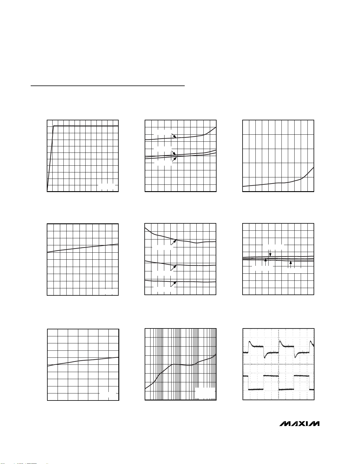
Typical Operating Characteristics
(VIN= +14V, CIN= 10µF, C
OUT
= 15µF, VEN= +2.4V, V
OUT
= +5V, SET = GND, TA= +25°C, unless otherwise specified.)
OUTPUT VOLTAGE
vs. INPUT VOLTAGE
MAX5023 toc01
VIN (V)
V
OUT
(V)
605545 5015 20 25 30 35 405 10
0.5
1.0
1.5
2.0
2.5
3.0
3.5
4.0
4.5
5.0
5.5
0
065
I
OUT
= 0mA
NO-LOAD GROUND CURRENT
vs. TEMPERATURE
MAX5023 toc02
TEMPERATURE (°C)
I
GND
(µA)
1109565 80-10 5 20 35 50-25
10
20
30
40
50
60
70
80
90
100
0
-40 125
VIN = +6.5V
VIN = +14V
VIN = +65V
8
11
14
17
20
5
SHUTDOWN SUPPLY CURRENT
vs. TEMPERATURE
MAX5023 toc03
TEMPERATURE (°C)
I
SHDN
(µA)
1109565 80-10 5 20 35 50-25-40 125
4.80
4.85
4.90
4.95
5.00
5.05
5.10
5.15
5.20
5.25
4.75
OUTPUT VOLTAGE
vs. TEMPERATURE
MAX5023 toc04
TEMPERATURE (°C)
V
OUT
(V)
1109565 80-10 5 20 35 50-25-40 125
I
OUT
= 1mA
0.25
0.50
0.75
1.00
1.25
1.50
1.75
2.00
2.25
0
GROUND CURRENT
vs. TEMPERATURE
MAX5023 toc05
TEMPERATURE (°C)
I
GND
(mA)
1109565 80-10 5 20 35 50-25-40 125
I
LOAD
= 50mA
I
LOAD
= 150mA
I
LOAD
= 100mA
V
OUT
(V)
4.6
4.7
4.8
4.9
5.0
5.1
5.2
5.3
5.4
5.5
4.5
OUTPUT VOLTAGE
vs. LOAD CURRENT AND TEMPERATURE
MAX5023 toc06
TEMPERATURE (°C)
1109565 80-10 5 20 35 50-25-40 125
I
LOAD
= 50mA
I
LOAD
= 150mA
I
LOAD
= 100mA
DROPOUT VOLTAGE
vs. LOAD CURRENT
MAX5023 toc07
I
LOAD
(mA)
DROPOUT VOLTAGE (V)
13011070 905030
0.15
0.30
0.45
0.60
0.75
0.90
1.05
1.20
1.35
1.50
0
10 150
V
OUT
= 5V
POWER-SUPPLY REJECTION RATIO
vs. FREQUENCY
MAX5023 toc08
FREQUENCY (kHz)
PSRR (dB)
100101
-70
-60
-50
-40
-30
-20
-10
0
-80
0.1 1000
C
OUT
= 15µF
I
OUT
= 10mA
LOAD-TRANSIENT RESPONSE
MAX5023 toc09
200µs/div
V
OUT
100mV/div
I
OUT
100mA/div
Page 5

MAX5023/MAX5024
65V, Low-Quiescent-Current, High-Voltage Linear
Regulators with µP Reset and Watchdog Timer
_______________________________________________________________________________________ 5
Typical Operating Characteristics (continued)
(VIN= +14V, CIN= 10µF, C
OUT
= 15µF, VEN= +2.4V, V
OUT
= +5V, SET = GND, TA= +25°C, unless otherwise specified.)
SHUTDOWN RESPONSE
MAX5023 toc16
40ms/div
V
EN
1V/div
V
OUT
2V/div
I
OUT
= 1mA
ENABLE AND HOLD TIMING
MAX5023 toc17
200ms/div
V
EN
5V/div
V
OUT
5V/div
V
HOLD
5V/div
INPUT VOLTAGE STEP RESPONSE
5V
V
OUT
1V/div
65V
V
IN
20V/div
6.5V
200µs/div
ENABLE STARTUP RESPONSE (VIN = +14V)
V
EN
1V/div
MAX5023 toc10
VEN = V
IN
I
= 1mA
OUT
MAX5023 toc13
STARTUP RESPONSE
VEN = V
IN
I
= 1mA
OUT
200µs/div
V
OUT
1V/div
65V
50V/div
5V
0V
V
IN
0V
ENABLE STARTUP RESPONSE (VIN = +65V)
V
EN
1V/div
MAX5023 toc11
MAX5023 toc14
V
1V/div
V
OUT
2V/div
V
1V/div
ENABLE STARTUP RESPONSE
= +14V)
(V
IN
EN
100µs/div
ENABLE STARTUP RESPONSE (VIN = +65V)
EN
MAX5023 toc12
I
OUT
MAX5023 toc15
= 0mA
V
OUT
2V/div
I
= 150mA
OUT
100µs/div
V
OUT
2V/div
100µs/div
I
= 0mA
OUT
V
OUT
2V/div
100µs/div
I
OUT
= 150mA
Page 6

MAX5023/MAX5024
65V, Low-Quiescent-Current, High-Voltage Linear
Regulators with µP Reset and Watchdog Timer
6 _______________________________________________________________________________________
Typical Operating Characteristics (continued)
(VIN= +14V, CIN= 10µF, C
OUT
= 15µF, VEN= +2.4V, V
OUT
= +5V, SET = GND, TA= +25°C, unless otherwise specified.)
0
10
5
20
15
25
30
45 5958 61 626053 5756 63 65 8964
GROUND-CURRENT DISTRIBUTION
(T
A
= +125°C)
MAX5023toc19
I
GND
(µA)
NUMBER OF UNITS
Pin Description
GROUND-CURRENT DISTRIBUTION
30
= +40°C)
(T
A
25
20
15
NUMBER OF UNITS
10
5
0
47 5453 56 575548 5251 58 60 6159 80
I
(µA)
GND
PIN
MAX5023 MAX5024
11IN
22EN
3 3 GND
NAME FUNCTION
Regulator Input. Supply voltage ranges from +6.5V to +65V. Bypass with a 10µF capacitor to
GND.
Enable Input. Force EN high to turn on the regulator. Pull EN low and force HOLD high (or
open circuit) to place the device in shutdown mode. Internally connected to ground through a
5MΩ resistor.
Ground. GND also functions as a heatsink. Solder to large pads or the circuit-board ground
plane to maximize thermal dissipation.
MAX5023toc18
Active-Low Open-Drain Reset Output. RESET remains low while V
44RESET
threshold or when WDI is not pulsed within 1.6s. RESET remains low for the duration of the
reset timeout period after the reset conditions are terminated.
Regulator Hold Input. When HOLD is forced low, the regulator stores the on state of the
55HOLD
output allowing the regulator to function even if EN is pulled low. To shutdown the regulator,
release HOLD after EN is pulled low. If HOLD is unused, either float HOLD or connect to OUT.
Internally connected to OUT through a 4µA pullup current source (see Table 1, Truth Table).
6 6 N.C. No Connection. Not internally connected.
7 — WDI
8 8 OUT
— 7 SET
Watchdog Timer Input (MAX5023 only). The watchdog timer asserts a reset if WDI does not
transition within the 1.6s watchdog timeout period. WDI cannot be disabled.
Regulator Output. Fixed (+3.3V or +5V) or adjustable (+2.5V to +11V). Bypass with a 15µF
capacitor (min).
Feedback Input for Setting the Output Voltage. Connect to GND to set the output voltage to
the preset fixed value (+3.3V or +5V). Connect to an external resistor-divider network for
adjustable output operation (MAX5024 only).
is below the reset
OUT
Page 7

Detailed Description
The MAX5023/MAX5024 high-voltage linear regulators
include an integrated µP reset circuit and watchdog
timer/adjustable output voltage. The devices guarantee
150mA load drive and are available with preset output
voltages of +3.3V or +5V. The MAX5023 features a
watchdog timer (WDI) with a 1.6s timeout period. The
MAX5024 offers an adjustable output voltage using an
external resistive-divider network between SET and
OUT. The internal reset circuit monitors the regulator
output voltage and asserts a reset output when the regulator output falls below the µP supply tolerance. Other
features include reverse-voltage protection to -60V,
enable (EN) and hold (HOLD) regulator control inputs,
16µA (max) shutdown current, short-circuit protection,
and thermal shutdown.
Regulator
The regulator accepts an input voltage range from
+6.5V to +65V. The MAX5023/MAX5024 offer fixed output voltages of +3.3V and +5V. The MAX5024 also features an adjustable output voltage that is implemented
with an external resistive-divider network connected
between OUT, SET, and GND (Figure 1). The MAX5024
automatically determines the feedback path depending
on the voltage at SET. Featured characteristics include
reverse-voltage protection to -60V and enable and hold
regulator control inputs. The Typical Operating Circuit
shows a self-holding configuration for the MAX5023.
MAX5023/MAX5024
65V, Low-Quiescent-Current, High-Voltage Linear
Regulators with µP Reset and Watchdog Timer
_______________________________________________________________________________________ 7
Functional Diagram
Figure 1. Functional Diagram
IN
HOLD
EN
+6.5V to +65V
OUT
4µA
CONTROL
LOGIC
REVERSE BATTERY PROTECTION
BANDGAP
REFERENCE
AMP
+2.5V to +11V
OUT
*MAX5023 ONLY.
WDI*
THERMAL
SENSOR
CURRENT
SENSOR AND
REGULATOR
COMP
TO INTERNAL SHUTDOWN
CIRCUITRY
WATCHDOG
TIMER AND
LOGIC
GND
MUX
R1
SET
(MAX5024 ONLY)
R2
RESET
200ms
TIMEOUT
PERIOD
Page 8

MAX5023/MAX5024
Reset Output
The reset supervisor circuit is fully integrated in the
MAX5023/MAX5024 and uses the same reference voltage as the regulator. RESET asserts during powerup/down and brownout conditions. RESET goes low if
V
OUT
drops below the preset output voltage threshold,
and remains low for 200ms (reset timeout period, tRP)
after V
OUT
rises above the reset voltage threshold. For
the MAX5023 only, RESET also asserts when WDI does
not transition for 1.6s (watchdog timeout period, tWD).
Two supply tolerance reset thresholds, -7.5% and
-12.5%, are available for each device type.
Watchdog Timer (MAX5023 only)
A watchdog timer asserts RESET if the watchdog input
(WDI) is not toggled for 1.6s (watchdog timeout period,
tWD). RESET remains low for 200ms (reset timeout peri-
od, tRP). If the watchdog is not updated for lengthy
periods of time, the reset output appears as a pulse
train, asserted for 200ms, deasserted for 1.6s, until WDI
is toggled again. Once RESET asserts, it stays low for
the entire reset timeout period ignoring any WDI transitions during the reset timeout period.
Figure 2 shows the Watchdog Operation Timing
Diagram. To prevent the watchdog from asserting
RESET, toggle WDI with a valid rising or falling edge
prior to t
WD
(min) = 1.12s. The watchdog counter clears
when WDI toggles prior to tWDor when RESET asserts.
The watchdog resumes counting after RESET deasserts.
Enable and Hold Inputs
The MAX5023/MAX5024 support two logic inputs, EN
(active high) and HOLD (active low), making these
devices “automotive friendly.” For example, the ignition
drives EN high, the regulator turns on and remains on
even if EN goes low, as long as HOLD is forced low
and stays low after initial regulator power-up. This feature makes it possible to implement a self-holding
circuit without external components. Release HOLD (an
internal current source connects HOLD to OUT) to turn
the regulator off.
Force EN low and HOLD high to place the MAX5023/
MAX5024 into shutdown mode. Shutdown mode draws
less than 16µA of supply current. Table 1 shows the state
of the regulator output with respect to the voltage level at
65V, Low-Quiescent-Current, High-Voltage Linear
Regulators with µP Reset and Watchdog Timer
8 _______________________________________________________________________________________
Figure 2. Watchdog Operation Timing Diagram
BATT
BATT
POR NORMAL OPERATION WDI HELD HIGH
BATT
V
WHEN WATCHDOG IS HELD
OUT
HIGH AND EN = HIGH
V
WDI
RESET
V
OUT
IN
EN
OV
OV
OV
V
IN
WHEN WATCHDOG IS HELD
V
OUT
LOW AND EN = HIGH
WDI
RESET
V
OUT
EN
OV
OV
OV
BATT
POR NORMAL OPERATION WDI HELD LOW
Page 9

EN and HOLD. Figure 3 shows the timing diagram for the
enable and hold functions. Connecting HOLD to OUT or
floating HOLD allows the EN input to act as a standard
ON/OFF switch for the regulator output.
Thermal Protection
When the junction temperature exceeds TJ= +150°C, an
internal thermal sensor signals the shutdown logic that
turns off the pass transistor and allows the IC to cool.
The thermal sensor turns the pass transistor on again
after the IC’s junction temperature cools by 20°C, resulting in a cycled output during continuous thermal-over-
load conditions. Thermal protection protects the
MAX5023/MAX5024 in the event of fault conditions. For
continuous operation, do not exceed the absolute maximum junction temperature rating of T
J
= +150°C.
Applications Information
Output Voltage Selection (MAX5024 only)
The MAX5024 features Dual Mode™operation: it operates in either a preset voltage mode or an adjustable
mode. In preset voltage mode, internal trimmed feedback resistors set the MAX5024’s internal linear
regulator to +3.3V or +5V (see the Selector Guide).
MAX5023/MAX5024
65V, Low-Quiescent-Current, High-Voltage Linear
Regulators with µP Reset and Watchdog Timer
_______________________________________________________________________________________ 9
Dual Mode is a trademark of Maxim Integrated Products, Inc.
Figure 3. Enable and Hold Behavior
V
IN
V
EN
V
V
V
HOLD, REL
V
HOLD, HOLD
EN, ON
EN, OFF
V
HOLD
1)
2)
5)
>10µs>10µs
4)
6)
7)
V
OUT
V
OUT (NOM)
V
RESET
0.2V
1) ENABLE ACTIVE
2) HOLD INACTIVE, PULLED UP BY V
3) POWER-ON RESET
4) HOLD ACTIVE, CLAMPED TO GND BY EXTERNAL µP
5) ENABLE INACTIVE, CLAMPED BY INT, PULLDOWN RESISTOR
200ms
3)
OUT
V
TH
8)
9)
6) PULSE WIDTH SMALLER THAN 10µs
7) HOLD INACTIVE, RELEASED BY µP
8) REGULATOR OUTPUT SHUTDOWN
9) OUTPUT-LOW RESET
Page 10

MAX5023/MAX5024
Select preset voltage mode by connecting SET to
ground. In adjustable mode, select an output between
+2.5V and +11V using two external resistors connected
as a voltage-divider to SET (Figure 4). Set the output
voltage using the following equation:
V
OUT
= V
SET
(1 + R1 / R2)
where V
SET
= 1.248V and R2 ≅ 100kΩ.
Available Output Current Calculation
The MAX5023/MAX5024 high-voltage regulator provides up to 150mA of output current. The input voltage
extends to +65V. Package power dissipation limits the
amount of output current available for a given input/
output voltage and ambient temperature. Figure 5
depicts the maximum power dissipation curve for these
devices. The graph assumes that the exposed metal
back of the MAX5023/MAX5024 package is soldered to
1in2of PC board copper.
Use Figure 5 to determine the allowable package dissipation for a given ambient temperature. Alternately, use
the following formula to calculate the allowable package dissipation:
After determining the allowable package dissipation,
calculate the maximum output current using the following formula:
The above equations do not include the negligible
power dissipation from self-heating due to the IC
ground current.
C
65V, Low-Quiescent-Current, High-Voltage Linear
Regulators with µP Reset and Watchdog Timer
10 ______________________________________________________________________________________
Figure 4. Setting the MAX5024 Adjustable Output Voltage
Figure 5. Maximum Power Dissipation vs. Temperature
Table 1. Truth Table for Regulator Output
State
X = Don’t care.
ORDER EN HOLD OUT COMMENTS
Initial state. EN has 5MΩ
1 Low X Off
2 High X On
3 High Low On
4 X Low On
5 Low High Off
P
=
D
W for T C
1 538 70
.
1 538 70 70 125
. - 0.01923 T - T
≤+ °
A
()
internal resistor to ground.
HOLD has internal current
source to OUT.
Regulator output is active
when EN is pulled high.
Hold is asserted forcing the
regulator output on even if
EN goes low.
S el f- hol d i ng state. Reg ul ator
outp ut stays on r eg ar d l ess of
the state of E N .
Regulator output is
shutdown by releasing
HOLD while EN remains low.
C for C
°
AA
+°< ≤+ °
+6.5V TO +65V +2.5V TO +11V
ON
OFF
TO µP
2.0
1.8
1.6
1.4
1.2
(W)
1.0
D
P
0.8
0.6
0.4
0.2
10 20 30 40 50 60 70 80 90 100 110 120 130 140 150
10µF
V
V
R2 = 1kΩ TO 500kΩ
1.538W
IN
EN
RESET
OUT
SET
MAX5024
= V
SET
= 1.248V
HOLD
GND
(1 + R1 / R2)
T
(°C)
A
OUT
15µF
R1
SET
R2
DERATE
19.23mW/°C
I
OUT MAX
()
P
D
≅≤
V
-V
OUT
IN
150
mA
Page 11

Example 1:
TA= +95°C
VIN= +14V
V
OUT
= +5V
Find the maximum allowable output current. First calculate package dissipation at the given temperature as
follows:
Then determine the maximum output current:
Example 2:
TA= +125°C
VIN= +14V
V
OUT
= +3.3V
Calculate package dissipation at the given temperature
as follows:
And establish the maximum current:
Example 3:
TA= +50°C
VIN= +14V
V
OUT
= +5V
Calculate package dissipation at the given temperature
as follows:
PD= 1.538W
And find the maximum output current:
In Example 3, the maximum output current is calculated
as 170.9mA, however, the maximum output current
cannot exceed 150mA. Use Figure 6 to quickly determine allowable maximum output current for selected
ambient temperatures.
Capacitor Selection and Regulator
Stability
For stable operation over the full temperature range
and with load currents up to 150mA, use a 15µF (min)
output capacitor with an ESR < 0.5Ω. To reduce noise
and improve load-transient response, stability, and
power-supply rejection, use larger output capacitor values such as 22µF.
Some ceramic dielectrics exhibit large capacitance
and ESR variation with temperature. For dielectric
capacitors such as Z5U and Y5V, use 22µF or more to
ensure stability at temperatures below -10°C. With X7R
or X5R dielectrics, 15µF should be sufficient at all operating temperatures. For high-ESR tantalum capacitors
use 22µF or more to maintain stability. To improve
power-supply rejection and transient response use a
minimum 10µF capacitor between IN and GND.
MAX5023/MAX5024
65V, Low-Quiescent-Current, High-Voltage Linear
Regulators with µP Reset and Watchdog Timer
______________________________________________________________________________________ 11
Figure 6. Maximum Output Current vs. Input Voltage
1 538
.
PW
=°
D
.
I
OUT MAX
- 0.01923W/ C 95 C - 70 C
()
=
1 057
1 057
()
=
()
V
14
()()
W
-5V
()
W
=
117 4..
°°
mA
1 538 25
.
PW
=°
D
.
I
OUT MAX
- 0.01923W/ C 1 C-70 C
()
=
480 4
mW
mW
480 4
()
=
()
V
14
- 3.3V
()( )
°°
()
44 89..
mA
=
I
OUT MAX OUT MAX
=
() ()
W
1 538
.
()
V
14
-5V
()()
mA I mA
=⇒ =
170 9 150
.
MAXIMUM OUTPUT CURRENT
vs. INPUT VOLTAGE
0.16
0.14
0.12
0.10
(A)
0.08
OUT(MAX)
I
0.06
0.04
0.02
TA = +125°C
0
070
V
= +5V
OUT
DEVICE EXPOSED
PAD SOLDERED TO
2
COPPER ISLAND
1IN
TA = +70°C
TA = +85°C
VIN (V)
MAX5023 fig04
65605 10 15 25 30 35 40 45 5020 55
Page 12

MAX5023/MAX5024
65V, Low-Quiescent-Current, High-Voltage Linear
Regulators with µP Reset and Watchdog Timer
12 ______________________________________________________________________________________
Selector Guide
Bold Items indicate standard versions. Samples are generally available on standard versions only. Contact factory for availability of nonstandard versions. Set MAX5024’s adjustable output voltage by connecting a resistive-divider from OUT to SET (see the Output Voltage
Selection section).
Chip Information
TRANSISTOR COUNT: 1382
PROCESS: BiCMOS
Typical Operating Circuit
PRESET V
PART
5V 3.3V 4.63V 4.38V 3.05V 2.89V
MAX5023L ✔ — ✔ ———✔ — ✔ —
MAX5023M ✔ —— ✔ ——— ✔✔ —
MAX5023T — ✔ ——✔ — ✔ — ✔ —
MAX5023S — ✔ ———✔ — ✔✔ —
MAX5024L ✔ — ✔ ———✔ —— ✔
MAX5024M ✔ —— ✔ ——— ✔ — ✔
MAX5024T — ✔ ——✔ — ✔ —— ✔
MAX5024S — ✔ ———✔ — ✔ — ✔
OUT
RESET THRESHOLD
(V
)
TH
RESET
V
OUT
TOLERANCE
V
-
OUT
7.5%
V
OUT
12.5%
WATCHDOG
-
TIMER
ADJUSTABLE
REGULATOR
OUTPUT
+6.5V TO +65V
IGNITION
ON
OFF
SWITCH
V
CC
RESET
I/OWDI
I/O
µP
10µF
IN
EN
HOLD
OUT
15µF
MAX5023
10kΩ
RESET
GND
Page 13

MAX5023/MAX5024
65V, Low-Quiescent-Current, High-Voltage Linear
Regulators with µP Reset and Watchdog Timer
Maxim cannot assume responsibility for use of any circuitry other than circuitry entirely embodied in a Maxim product. No circuit patent licenses are
implied. Maxim reserves the right to change the circuitry and specifications without notice at any time.
Maxim Integrated Products, 120 San Gabriel Drive, Sunnyvale, CA 94086 408-737-7600 ____________________ 13
© 2002 Maxim Integrated Products Printed USA is a registered trademark of Maxim Integrated Products.
Package Information
(The package drawing(s) in this data sheet may not reflect the most current specifications. For the latest package outline information
go to www.maxim-ic.com/packages.)
8L, SOIC EXP. PAD.EPS
 Loading...