

Datasheet MAX5021EUT, MAX5022EUT, MAX5021EPA, MAX5021EUA, MAX5022EPA Datasheet (Maxim) [ru]
...
General Description
The MAX5021/MAX5022 current-mode PWM controllers
contain all the control circuitry required for the design
of wide input voltage range isolated power supplies.
These devices are well suited for use in universal input
(85VAC to 265VAC) off-line or telecom (-36VDC to
-72VDC) power supplies.
An undervoltage lockout (UVLO) circuit with large hysteresis coupled with low startup and operating current
reduce power dissipation in the startup resistor and
allow use of ceramic bypass capacitors. The 262kHz
switching frequency is internally trimmed to ±12%
accuracy; this allows the optimization of the magnetic
and filter components resulting in compact, cost-effective power supplies. The MAX5021 with 50% maximum
duty cycle and MAX5022 with 75% maximum duty
cycle are recommended for forward converters and flyback converters, respectively. The MAX5021/MAX5022
are available in 6-pin SOT23, 8-pin µMAX, and 8-pin
DIP packages and are rated for operation over the
-40°C to +85°C temperature range.
Applications
Universal Off-Line Power Supplies
Standby Power Supplies
Isolated Power Supplies
Isolated Telecom Power Supplies
Mobile Phone Chargers
Features
♦ Available in a Tiny 6-Pin SOT23 Package
♦ 50µA Typical Startup Current
♦ 1.2mA Typical Operating Current
♦ Large UVLO Hysteresis of 14V
♦ Fixed Switching Frequency of 262kHz ±12%
♦ 50% Maximum Duty Cycle Limit (MAX5021)
♦ 75% Maximum Duty Cycle Limit (MAX5022)
♦ 60ns Cycle-by-Cycle Current-Limit Response
Time
MAX5021/MAX5022
Current-Mode PWM Controllers for Isolated
Power Supplies
________________________________________________________________ Maxim Integrated Products 1
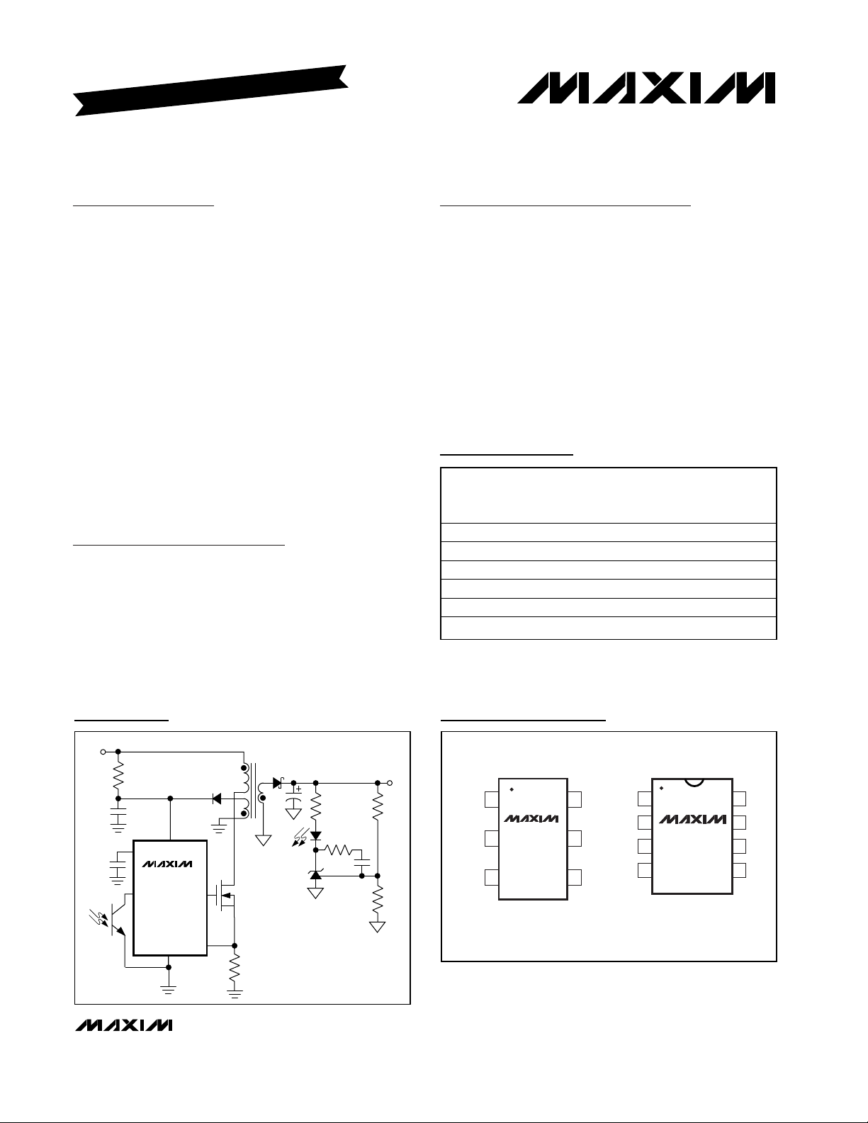
Pin Configuration
Ordering Information
MAX5021
MAX5022
V
OUT
V
SUPPLY
OPTO NDRV
CS
V
CC
V
IN
GND
Typical Operating Circuit
19-2066; Rev 1; 9/01
EVALUATION KIT AVAILABLE
For pricing, delivery, and ordering information, please contact Maxim/Dallas Direct! at
1-888-629-4642, or visit Maxim’s website at www.maxim-ic.com.
WARNING: The MAX5021/MAX5022 are designed to work
with high voltages. Exercise caution!
MAX
PART
MAX5021EUT 50% -40°C to +85°C 6 SOT23-6 AASQ
MAX5021EUA 50% -40°C to +85°C 8 µMAX —
MAX5021EPA 50% -40°C to +85°C 8 PDIP —
MAX5022EUT 75% -40°C to +85°C 6 SOT23-6 AASR
MAX5022EUA 75% -40°C to +85°C 8 µMAX —
MAX5022EPA 75% -40°C to +85°C 8 PDIP —
DUTY
CYCLE
TEMP.
RANGE
PIN PACKAGE
TOP
MARK
TOP VIEW
16OPTO
CS
GND
NDRV
MAX5021
2
MAX5022
34
SOT23
1
OPTO
2
5 V
IN
IN
V
CC
V
CC
3
4
PDIP/µMAX
MAX5021
MAX5022
87CS
6
5
GNDV
NDRV
N.C.N.C.
MAX5021/MAX5022
Current-Mode PWM Controllers for Isolated
Power Supplies
2 _______________________________________________________________________________________
ABSOLUTE MAXIMUM RATINGS
ELECTRICAL CHARACTERISTICS
(VIN= +11V to +28V, VCS= 0, OPTO is unconnected, 10nF bypass capacitors at VINand VCC, NDRV unconnected, TA= -40°C to
+85°C, unless otherwise noted. Typical values are at V
IN
= +12V, TA= +25°C, unless otherwise noted.) (Note 1)
Stresses beyond those listed under “Absolute Maximum Ratings” may cause permanent damage to the device. These are stress ratings only, and functional
operation of the device at these or any other conditions beyond those indicated in the operational sections of the specifications is not implied. Exposure to
absolute maximum rating conditions for extended periods may affect device reliability.
VINto GND .............................................................-0.3V to +30V
V
CC
to GND............................................................-0.3V to +13V
NDRV to GND.............................................-0.3V to (V
CC
+ 0.3V)
CS, OPTO to GND ....................................................-0.3V to +6V
NDRV Short-Circuit to GND........................................Continuous
Continuous Power Dissipation (T
A
= +70°C)
6-Pin SOT23 (derate 8.7mW/°C above +70°C).............696mW
8-Pin µMAX (derate 4.5mW/°C above +70°C) ..............362mW
8-Pin PDIP (derate 9.1mW/°C above +70°C)................727mW
Operating Temperature Range ...........................-40°C to +85°C
Storage Temperature Range .............................-55°C to +150°C
Lead Temperature (soldering 10s) ..................................+300°C
)
)
)
UNDERVOLTAGE LOCKOUT/STARTUP
CURRENT-LIMIT COMPARATOR
PARAMETER SYMBOL CONDITIONS MIN TYP MAX UNITS
Undervoltage Lockout Wakeup
Level
Undervoltage Lockout Shutdown
Level
VIN Supply Current at Startup I
VIN Range V
Undervoltage Lockout
Propagation Delay
INTERNAL SUPPLY
VCC Regulator Set Point V
VIN Supply Current after Startup I
GATE DRIVER
Driver Output Impedance
Driver Peak Sink Current I
Driver Peak Source Current I
PWM COMPARATOR
Comparator Offset Voltage VO
CS Input Bias Current I
Propagation Delay from
Comparator Input to NDRV
Minimum On-Time T
Current-Limit Trip Threshold V
Current-Limit Propagation Delay
from Comparator Input to NDRV
V
V
STARTVIN
T
T
R
ON(LOW
R
ON(HIGH
SOURCE
T
ON(MIN
UVR
UVF
UVR
UVF
CCSP
SINK
PWM
T
VIN rising 22 24 26 V
VIN falling 9.3 10 10.9 V
IN
VIN steps up from +9V to +26V 5
VIN steps down from +26V to +9V 1
VIN = +11V to +28V, sourcing 1µA to 5mA
from V
VIN = +28V, OPTO connected to GND 0.9 2.43
IN
VIN = +28V, OPTO unconnected (Note 2) 0.4
Measured at NDRV sinking 5mA 10 20
Measured at NDRV sourcing 5mA 20 40
PWMVOPTO
CS
25mV overdrive 60 ns
CS
25mV overdrive 60 ns
CL
= +22V 50 85 µA
CC
- V
CS
11 28 V
7.0 10.5 V
250 mA
150 mA
600 750 900 mV
-2 +2 µA
150 ns
540 600 660 mV
µs
mA
Ω
MAX5021/MAX5022
Current-Mode PWM Controllers for Isolated
Power Supplies
_______________________________________________________________________________________ 3
ELECTRICAL CHARACTERISTICS (continued)
(VIN= +11V to +28V, VCS= 0, OPTO is unconnected, 10nF bypass capacitors at VINand VCC, NDRV unconnected, TA= -40°C to
+85°C, unless otherwise noted. Typical values are at V
IN
= +12V, TA= +25°C, unless otherwise noted.) (Note 1)
Note 1: All devices are 100% tested at T
A
= +25°C. All limits over temperature are guaranteed by characterization.
Note 2: This minimum current after startup is a safeguard that prevents the V
IN
pin voltage from rising in the event
that OPTO and NDRV become unconnected.
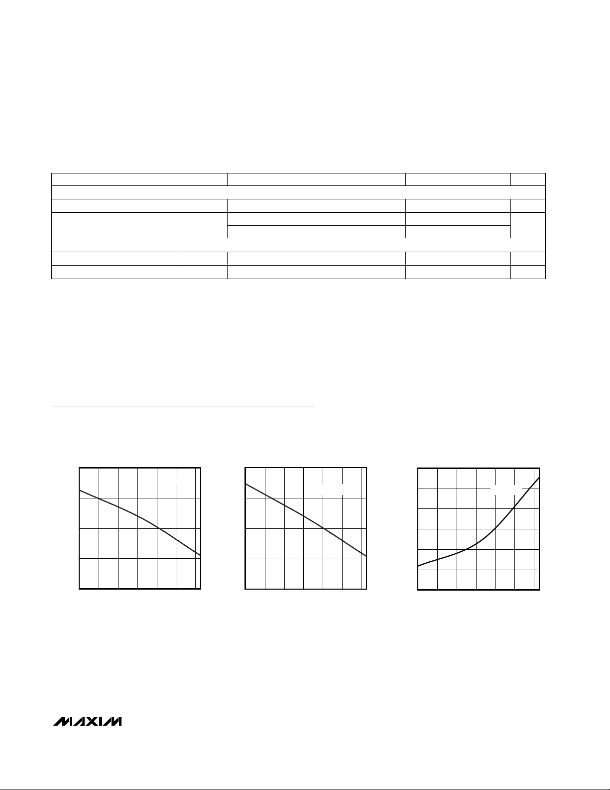
Typical Operating Characteristics
(VIN= 15V, TA = +25°C, unless otherwise noted.)
23.9
24.0
24.1
24.2
24.3
UNDERVOLTAGE LOCKOUT
vs. TEMPERATURE
MAX5021/22 toc01
TEMPERATURE (°C)
UNDERVOLTAGE LOCKOUT (V)
-40 20 40-20 0 60 80
VIN RISING
9.8
9.9
10.0
10.1
10.2
UNDERVOLTAGE LOCKOUT
vs. TEMPERATURE
MAX5021/22 toc02
TEMPERATURE (°C)
UNDERVOLTAGE LOCKOUT (V)
-40 20 40-20 0 60 80
VIN FALLING
47
48
49
50
51
52
53
-40 -20 0 20 40 60 80
STARTUP CURRENT
vs. TEMPERATURE
MAX5021/22 toc03
TEMPERATURE (°C)
STARTUP CURRENT (µA)
VIN = 23.0V
PARAMETER SYMBOL CONDITIONS MIN TYP MAX UNITS
OSCILLATOR
Switching Frequency f
Maximum Duty Cycle D
SW
MAX
MAX5021 50 51
MAX5022 75 76
OPTO INPUT
OPTO Pullup Voltage V
OPTO Pullup Resistance R
OPTO
OPTO
OPTO sourcing 10µA 5.5 V
230 262 290 kHz
4.5 6.2 7.9 kΩ
%
MAX5021/MAX5022
Current-Mode PWM Controllers for Isolated
Power Supplies
4 _______________________________________________________________________________________
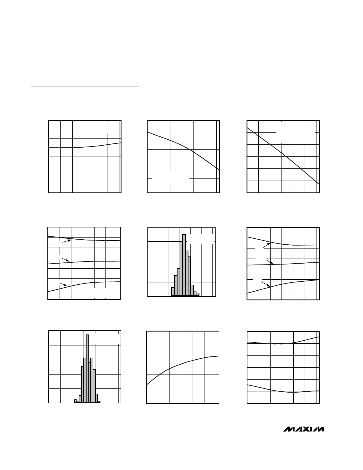
Typical Operating Characteristics (continued)
(VIN= 15V, TA = +25°C, unless otherwise noted.)
1.40
1.45
1.50
1.55
1.60
SUPPLY CURRENT
vs. TEMPERATURE
MAX5021/22 toc04
TEMPERATURE (°C)
SUPPLY CURRENT (mA)
-40 20 40-20 0 60 80
VIN = 28.0V
V
OPTO
= VCS = 0
9.00
9.03
9.09
9.06
9.12
9.15
-40 0-20 20 40 60 80
MAXIMUM VCC
vs. TEMPERATURE
MAX5021/22 toc05
TEMPERATURE (°C)
MAXIMUM V
CC
(V)
VIN = 28.0V
V
CS
= 0
OPTO = UNCONNECTED
7.70
7.90
7.80
8.10
8.00
8.20
8.30
-40 20 40-20 0 60 80
MINIMUM VCC
vs. TEMPERATURE
MAX5021/22 toc06
TEMPERATURE (°C)
MINIMUM V
CC
(V)
VIN = 10.8V
5mA LOAD ON V
CC
VCS = 0
OPTO = UNCONNECTED
570
590
580
610
600
630
620
640
-40 0 20-20 40 60 80
CURRENT SENSE THRESHOLD
vs. TEMPERATURE
MAX5021/22 toc07
TEMPERATURE (°C)
CURRENT SENSE THRESHOLD (mV)
+3σ
-3σ
MEAN
TOTAL NUMBER OF
DEVICES = 50
0
5
15
10
20
25
540 580560 620
640 660
CURRENT SENSE
THRESHOLD
MAX5021/22 toc08
CURRENT SENSE THRESHOLD (mV)
FREQUENCY (%)
TOTAL NUMBER
OF DEVICES = 200
600
245
255
250
265
260
275
270
280
-40 0 20-20 40 60 80
OSCILLATOR FREQUENCY
vs. TEMPERATURE
MAX5021/22 toc09
TEMPERATURE (°C)
OSCILLATOR FREQUENCY (kHz)
TOTAL NUMBER
OF DEVICES = 50
+3σ
-3σ
MEAN
0
5
15
10
20
25
230 250240 260 270 280 290
OSCILLATOR FREQUENCY
MAX5021/22 toc10
OSCILLATOR FREQUENCY (kHz)
FREQUENCY (%)
TOTAL NUMBER
OF DEVICES = 200
50
55
65
60
70
75
-40 0-20 20 40 60 80
CURRENT SENSE DELAY
vs. TEMPERATURE
MAX5021/22 toc11
TEMPERATURE (°C)
CURRENT SENSE DELAY (ns)
0
2
1
4
3
5
6
-40 20 40-20 0 60 80
UNDERVOLTAGE LOCKOUT
DELAY vs. TEMPERATURE
MAX5021/22 toc12
TEMPERATURE (°C)
UNDERVOLTAGE LOCKOUT DELAY (µs)
VIN RISING
VIN FALLING

Detailed Description
The MAX5021/MAX5022 are current-mode PWM controllers that have been specifically designed for use in
isolated power supplies. An undervoltage lockout circuit (UVLO) with a large hysteresis (14V) along with
very low startup and operating current result in highefficiency, universal input power supplies. Both devices
can be used in power supplies capable of operating
from a universal 85VAC to 265VAC line or the telecom
voltage range of -36VDC to -72VDC.
Power supplies designed with these devices use a
high-value startup resistor, RS, (series combination of
R1and R2) that charges a reservoir capacitor, C2 (see
Figure 1). During this initial period while the voltage is
less than the UVLO start threshold, the IC typically consumes only 50µA of quiescent current. This low startup
current and the large UVLO hysteresis combined with
the use of a ceramic capacitor C2 keeps the power dissipation in RSto less than 1/4W even at the high end of
the universal AC input voltage (265VAC).
The MAX5021/MAX5022 include a cycle-by-cycle current limit which turns off the gate drive to the external
MOSFET during an overcurrent condition. If the output
on the secondary side of transformer T1 is shorted, the
tertiary winding voltage will drop below the 10V threshold causing the UVLO circuit to turn off the gate drive to
the external power MOSFET, thus re-initiating the startup sequence.
Startup
Figure 2 shows the voltages on VINand VCCduring
startup. Initially, both VINand VCCare 0V. After the line
voltage is applied, C2 charges through the startup
resistor, RS, to an intermediate voltage at which point
the internal reference and regulator begin charging C3
(see Figure 1). The bias current consumed by the
device during this period is only 50µA; the remaining
input current charges C2 and C3. Charging of C3 stops
when the VCCvoltage reaches approximately 9.5V,
while the voltage across C2 continues rising until it
reaches the wakeup level of 24V. Once VINexceeds
the UVLO threshold, NDRV begins switching the
MOSFET, transferring energy to the secondary and tertiary outputs. If the voltage on the tertiary output builds
to higher than 10V (UVLO lower threshold), then startup
has been accomplished and sustained operation
will commence.
If VINdrops below 10V before startup is complete, then
the IC goes back into UVLO. In this case, increase the
value of C2 and/or use a MOSFET with a lower gatecharge requirement.
Startup Time Considerations
The VINbypass capacitor C2 supplies current immediately after wakeup. The size of C2 will determine the number
of cycles available for startup. Large values for C2 will
increase the startup time, but will also supply more gate
charge, allowing for more cycles after wakeup. If the
value of C2 is too small, VINwill drop below 10V because
MAX5021/MAX5022
Current-Mode PWM Controllers for Isolated
Power Supplies
_______________________________________________________________________________________ 5
Pin Description
PIN
SOT23
18CS
2 7 GND Power-Supply Ground
3 6 NDRV External N-Channel MOSFET Gate Connection
43V
52V
6 1 OPTO
— 4, 5 N.C. No Connection. Do not make connections to these pins.
PDIP
µMAX
NAME FUNCTION
C ur r ent S ense C onnecti on for P WM Reg ul ati on and Over cur r ent P r otecti on. The cur r ent- l i m i t
com p ar ator thr eshol d i s i nter nal l y set to 0.6V .
CC
IN
Gate Drive Supply. Internally regulated down from VIN. Decouple with a 10nF or larger
capacitor to GND.
IC Supply. Decouple with a 10nF or larger capacitor to GND. Connect a startup resistor
) from the input supply line to VIN. Connect to bias winding through diode rectifier.
(R
s
See Typical Operating Circuit.
Optocoupler Transistor Collector Connection. Connect emitter of optocoupler to GND.
The OPTO has an internal pullup resistor with a typical value of 6.2kΩ.

MAX5021/MAX5022
NDRV did not switch enough times to build up sufficient
voltage across the tertiary output to power the device.
The device will go back into UVLO and will not start. Use
a low-leakage ceramic or film capacitor for C2 and C3.
As a rule of thumb, off-line power supplies keep typical
startup times to less than 500ms even in low-line conditions (85VAC input). Size the startup resistor, R
S
, to supply the maximum startup bias of the IC (85µA) plus the
additional current required for charging the capacitors
C2 and C3 in less than 500ms. This resistor dissipates
continuous power in normal operation, despite the fact
that it is only used during the startup sequence.
Therefore it must be chosen to provide enough current
for the low-line condition as well as have an appropriate
power rating for the high-line condition (265VAC). In
most cases, split the value into two resistors connected
in series for the required voltage of approximately
400VDC.
The typical value for C2 and C3 is 220nF. The startup
resistor, RS, provides both the maximum quiescent current of 85µA and the charging current for C2 and C3.
Bypass capacitor C3 charges to 9.5V and C2 charges
to 24V all within the desired time period of 500ms, for
an overall average charging current of 15µA. Hence,
the startup resistor must provide a total of at least
100µA. Developing 100µA from an input voltage of
Current-Mode PWM Controllers for Isolated
Power Supplies
6 _______________________________________________________________________________________
Figure 1. Universal 5W Off-Line Standby Power Supply
Figure 2. VINand VCCDuring Startup
CENTRAL SEMICONDUCTOR
CBR1-D100S
L
85VAC TO
265VAC IN
N
G
AC
C1
AC
10µF
400V
OPTO
CNY17-3
0.22µF
250mA, 75V
CMPD914
C3
CENTRAL SEMICONDUCTOR
FAIRCHILD
L2
470µH
R8
1.2kΩ
D1
V
CC
MAX5022
OPTO NDRV
U1
C9
10µF
400V
R1
360kΩ
RS = R1 + R2
R2
360kΩ
C2
0.22µF
V
IN
CTX03-15256
480µH, 60T
D1
R11
10Ω
8T
N1
INTERNATIONAL RECTIFIER
IRFRC20
T1
ON SEMICONDUCTOR
3T
C7
1000pF
D2
3A, 40V
MBRS340T3
C4
150µF
6.3V
INSTRUMENTS
1kΩ
OPTO
TEXAS
TLV431AIDBV
1%
R3
R10
10Ω
0.01µF
24.9kΩ
C5
8.06kΩ
1%
1%
+5V OUT
C6
R4
0.1µF
R5
CS
GND
240kΩ
R9
8200pF
C8
NOTE: ALL RESISTORS ARE 5% UNLESS OTHERWISE SPECIFIED.
R6
10Ω
R
CS
1.78Ω
1%
25
20
15
(V)
CC
, V
IN
10
V
5
0
0 10050 150 200
V
IN
V
CC
IC COMES OUT OF UVLO
(WAKEUP)
SUPPLIED BY C2
V
IN
SUPPLIED BY TERTIARY
V
IN
WINDING (NORMAL OPERATION)
V
BYPASS CAPACITOR
CC
FULLY CHARGED
DROPS SLIGHTLY WHEN
V
CC
NDRV BEGINS SWITCHING
TIME (ms)

85VAC (corresponding to 120VDC) to the 24V wakeup
level results in a resistor value of about 1MΩ. If we
assume RSvalues between 750kΩ and 1MΩ, then at
the high-line voltage of 265VAC (corresponding to
374VDC) power dissipation will be between 140mW to
190mW. A single 1/4W resistor or a series combination
of two 1/4W resistors is adequate.
Undervoltage Lockout (UVLO)
The device will attempt to start when VINexceeds the
UVLO threshold of 24V. During startup, the UVLO circuit keeps the CPWM comparator, ILIM comparator,
oscillator, and output driver shut down to reduce current consumption (Functional Diagram). Once V
IN
reaches 24V, the UVLO circuit turns on both the CPWM
and ILIM comparators, as well as the oscillator, and
allows the output driver to switch. If VINdrops below
10V, the UVLO circuit will shut down the CPWM comparator, ILIM comparator, oscillator, and output driver
returning the MAX5021/MAX5022 to the startup mode.
N-Channel MOSFET Switch Driver
The NDRV pin drives an external N-channel MOSFET.
The NDRV output is supplied by the internal regulator
(VCC), which is internally set to approximately 9V. For
the universal input voltage range, the MOSFET used
must be able to withstand the DC level of the high-line
input voltage plus the reflected voltage at the primary
of the transformer. For most applications that use the
discontinuous flyback topology, this requires a MOSFET rated at 600V. NDRV can source/sink 150mA/
250mA peak current, thus select a MOSFET that will
yield acceptable conduction and switching losses.
Internal Oscillator
The internal oscillator switches at 1.048MHz and is
divided down to 262kHz by two D flip-flops. The
MAX5021 inverts the Q output of the last D flip-flop to
provide a duty cycle of 50% (Figure 3). The MAX5022
performs a logic NAND operation on the Q outputs of
both D flip-flops to provide a duty cycle of 75%.
Optocoupler Feedback
The MAX5021/MAX5022 do not include an internal error
amplifier and are recommended for use in optocoupler
feedback power supplies. Isolated voltage feedback is
achieved by using an optocoupler and a shunt regulator as shown in the Typical Operating Circuit. The output voltage set point accuracy is a function of the
accuracy of the shunt regulator and resistor divider.
When a TLV431 shunt regulator is used for output voltage regulation, the output voltage is set by the ratio of
R4 and R5 (Figure 1). Output voltage is given by the
following equation:
where V
REF
= 1.24V for the TLV431.
During normal operation, the optocoupler feedback pin
(OPTO) is pulled up through a 6.2kΩ resistor to the
internal supply voltage of 5.25V. When the device is in
UVLO, OPTO is disconnected from the 5.25V regulator
and connected to ground (Functional Diagram). This
helps initial startup by reducing the current consumption of the device.
Current Limit
The current limit is set by a current sense resistor, RCS,
connected between the source of the MOSFET and
ground. The CS input has a voltage trip level (VCS) of
600mV. Use the following equation to calculate the
value of RCS:
where I
PRI
is the peak current in the primary that flows
through the MOSFET. When the voltage produced by
this current through the current sense resistor exceeds
the current-limit comparator threshold, the MOSFET driver (NDRV) will quickly terminate the current ON-cycle,
typically within 60ns. In most cases a small RC filter will
be required to filter out the leading-edge spike on the
sense waveform. Set the corner frequency at a
few MHz.
Applications Information
Universal Off-Line Power Supply
Figure 1 shows the design of a 5V/1A isolated power
supply capable of operating from a line voltage of
85VAC to 265VAC. This circuit is implemented in the
MAX5022EVKIT.
MAX5021/MAX5022
Current-Mode PWM Controllers for Isolated
Power Supplies
_______________________________________________________________________________________ 7
Figure 3. Internal Oscillator
DQ
OSCILLATOR
1.048MHz
Q
DQ
Q
262kHz WITH 50%
(MAX5021)
262kHz WITH 75%
(MAX5022)
R
4
VV
=×+
OUT REF
1
R
5
V
CS
CS
=
I
PRI
R

MAX5021/MAX5022
WARNING! DANGEROUS AND LETHAL VOLTAGES
ARE PRESENT IN OFF-LINE CIRCUITS! USE
EXTREME CAUTION IN THE CONSTRUCTION,
TESTING, AND USE OF OFF-LINE CIRCUITS.
Isolated Telecom Power Supply
Figure 4 shows a -48VDC telecom power supply capable of generating an isolated +5V output.
Layout Recommendations
All printed circuit board traces carrying switching currents must be kept as short as possible, and the current loops they form must be minimized. The pins of the
SOT23 package have been placed to allow simple
interfacing to the external MOSFET. The order of these
pins directly corresponds to the order of a TO-220 or
similar package MOSFET.
For universal AC input design all applicable safety regulations must be followed. Off-line power supplies may
require UL, VDE, and other similar agency approvals.
These agencies can be contacted for the latest layout
and component rules.
Typically there are two sources of noise emission in a
switching power supply: high di/dt loops and high dv/dt
surfaces. For example, traces that carry the drain current often form high di/dt loops. Similarly the heatsink of
the MOSFET presents a dv/dt source, thus the surface
area of the heatsink must be minimized as much
as possible.
To achieve best performance, a star ground connection
is recommended to avoid ground loops. For example,
the ground returns for the power-line input filter, power
MOSFET switch, and sense resistor should be routed
separately through wide copper traces to meet at a single system ground connection.
Chip Information
TRANSISTOR COUNT: 519
PROCESS: BiCMOS
Current-Mode PWM Controllers for Isolated
Power Supplies
8 _______________________________________________________________________________________
Figure 4. -48VDC Input to +5V Output
T1
V
R
S
C2
OUT
V
IN
CS
-36VDC TO -72VDC IN
V
C3
CC
MAX5022
OPTO NDRV
GND

MAX5021/MAX5022
Current-Mode PWM Controllers for Isolated
Power Supplies
_______________________________________________________________________________________ 9
Functional Diagram
V
OPTO
IN
IN
REFERENCE
1.25V
GND
6.2kΩ
0.75V
CS
VO
V
CS
0.6V
CPWM
PWM
ILIM
OSCILLATOR
262kHz*
*MAX5021: 50% MAXIMUM DUTY CYCLE
MAX5022: 75% MAXIMUM DUTY CYCLE
UVLO
24V
10V
S
R
IN
REGULATOR
REG_OK
Q
V
CC
V
L
(INTERNAL 5.25V
SUPPLY)
DRIVER
V
CC
NDRV
GND

MAX5021/MAX5022
Current-Mode PWM Controllers for Isolated
Power Supplies
10 ______________________________________________________________________________________
Package Information
6LSOT.EPS
PROPRIETARY INFORMATION
TITLE:
PACKAGE OUTLINE, 8L uMAX/uSOP
21-0036
REV.DOCUMENT CONTROL NO.APPROVAL
1
J
1

MAX5021/MAX5022
Current-Mode PWM Controllers for Isolated
Power Supplies
Maxim cannot assume responsibility for use of any circuitry other than circuitry entirely embodied in a Maxim product. No circuit patent licenses are
implied. Maxim reserves the right to change the circuitry and specifications without notice at any time.
Maxim Integrated Products, 120 San Gabriel Drive, Sunnyvale, CA 94086 408-737-7600 ____________________ 11
© 2001 Maxim Integrated Products Printed USA is a registered trademark of Maxim Integrated Products.
Package Information (continued)
PDIPN.EPS

 Loading...