

Page 1
现货库存、技术资料、百科信息、热点资讯,精彩尽在鼎好!
General Description
The MAX5019/MAX5020 integrate all the building
blocks necessary for implementing DC-DC fixed-frequency power supplies. Either primary- or secondaryside regulation may be used to implement isolated or
nonisolated power supplies. These devices are currentmode controllers with an integrated high-voltage startup circuit suitable for telecom/industrial voltage range
power supplies. Current-mode control with leadingedge blanking simplifies control-loop design and internal ramp compensation circuitry stabilizes the current
loop when operating at duty cycles above 50%
(MAX5019). The MAX5019 allows 85% operating duty
cycle and can be used to implement flyback converters
whereas the MAX5020 limits the operating duty cycle to
less than 50% and can be used in single-ended forward converters. A high-voltage startup circuit allows
these devices to draw power directly from the 18V to
110V input supply during startup. The switching frequency is internally trimmed to 275kHz ±10%, thus
reducing magnetics and filter component costs.
The MAX5019/MAX5020 are available in 8-pin SO
packages.
Warning: The MAX5019/MAX5020 operate with high
voltages. Exercise caution.
Applications
Telecom Power Supplies
Industrial Power Supplies
Networking Power Supplies
Isolated Power Supplies
Features
♦ Wide Input Range: (18V to 110V) or (13V to 36V)
♦ Isolated (without optocoupler) or Nonisolated
Power Supply
♦ Current-Mode Control
♦ Leading-Edge Blanking
♦ Internally Trimmed 275kHz ±10% Oscillator
♦ Low External Component Count
♦ Soft-Start
♦ High-Voltage Startup Circuit
♦ Pulse-by-Pulse Current Limiting
♦ Thermal Shutdown
♦ SO-8 Package
MAX5019/MAX5020
Current-Mode PWM Controllers with Integrated
Startup Circuit
________________________________________________________________ Maxim Integrated Products 1
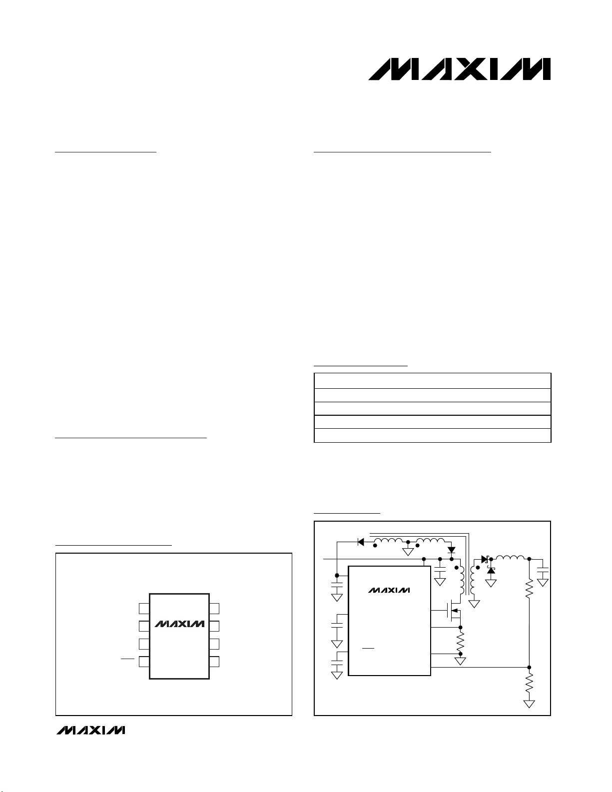
Pin Configuration
Ordering Information
NDRV
V
IN
V
OUT
V
DD
V
CC
CS
FB
MAX5020
V+
SS_SHDN
GND
Typical Operating Circuit
19-2115; Rev 0; 7/01
For pricing, delivery, and ordering information, please contact Maxim/Dallas Direct! at
1-888-629-4642, or visit Maxim’s website at www.maxim-ic.com.
*See Selector Guide at end of data sheet.
PART TEMP. RANGE PIN-PACKAGE
MAX5019CSA* 0°C to +70°C8-SO
MAX5019ESA* -40°C to +85°C8-SO
MAX5020CSA* 0°C to +70°C8-SO
MAX5020ESA* -40°C to +85°C8-SO
TOP VIEW
V+
1
2
DD
FB
SS_SHDN
3
4
MAX5019/
MAX5020
8-SO
87V
6
5
CC
NDRVV
GND
CS
Page 2

MAX5019/MAX5020
Current-Mode PWM Controllers with Integrated
Startup Circuit
2 _______________________________________________________________________________________
ABSOLUTE MAXIMUM RATINGS
ELECTRICAL CHARACTERISTICS
(VDD= 13V, a 10µF capacitor connects VCCto GND, VCS= 0, V+ = 48V, 0.1µF capacitor connected from SS_SHDN to GND, NDRV
= open circuit, V
FB
= 3V, TA= -40°C to +85°C, unless otherwise noted. Typical values are at TA= +25°C.)
Stresses beyond those listed under “Absolute Maximum Ratings” may cause permanent damage to the device. These are stress ratings only, and functional
operation of the device at these or any other conditions beyond those indicated in the operational sections of the specifications is not implied. Exposure to
absolute maximum rating conditions for extended periods may affect device reliability.
V+ to GND……………………………………...……-0.3V to +120V
V
DD
to GND.………………………………….……….-0.3V to +40V
V
CC
to GND.………………….……………………-0.3V to +12.5V
FB, NDRV, SS_SHDN, CS to GND .……-0.3V to V
CC
+ 0.3V
V
DD
and VCCCurrent …………………...…………………..20mA
NDRV Current Continuous...………………………………….25mA
NDRV Current for Less than 1µs..………….…………….……±1A
Continuous Power Dissipation (T
A
= +70°C)
8-Pin SO (derate 5.88mW/°C above +70°C) .………....471mW
Operating Temperature Range…………..……...-40°C to +85°C
Storage Temperature Range……………..…….-65°C to +150°C
Lead Temperature (soldering, 10s) ………………………+300°C
)
PARAMETER SYMBOL CONDITIONS MIN TYP MAX UNITS
SUPPLY CURRENT
V+ Supply Current
V+ Supply Current After Startup V+ = 110V, VDD = 13V, FB = GND 14 µA
V
S up p l y C ur r ent
D D
V+ Shutdown Current V
VDD Shutdown Current V
PREREGULATOR/STARTUP
V+ Input Voltage 18 110 V
V
Supply Voltage 13 36 V
DD
INTERNAL REGULATORS (VCC)
VCC Output Voltage
VCC Undervoltage Lockout V
OUTPUT DRIVER
Peak Source Current VCC = 11V (externally forced) 570 mA
Peak Sink Current VCC = 11V (externally forced) 1000 mA
NRDV High-Side Driver
Resistance
I
V+(NS)
I
V+(S)
I
VDD(NS
I
VDD(S)
CC_UVLOVCC
R
OH
VDD = 0, V+ = 110V, driver not switching 0.8 1.6
V+ = 110V, VDD = 0, FB = GND,
driver switching
VDD = 36V, driver not switching 0.9 1.6
VDD = 36V, driver switching, FB = GND 2.1 3.0
SS_SHDN
SS_SHDN
Powered from V+, ICC = 7.5mA, VDD = 0 7.5 9.8 12.0 V
Powered from V
VCC = 11V, externally forced,
NDRV sourcing 50mA
= 0, V+ = 110V 180 290 µA
= 0 4 20 µ A
, ICC = 7.5mA 9.0 10.0 11.0 V
DD
falling 6.6 V
1.6 3.0
412Ω
mA
mA
NDRV Low-Side Driver
Resistance
ERROR AMPLIFIER
FB Input Resistance R
FB Input Bias Current I
Error Amplifier Gain (Inverting) A
Closed-Loop 3dB Bandwidth 200 kHz
FB Input Voltage Range 23V
R
OL
IN
FB
VCL
VCC = 11V, externally forced,
NDRV sinking 50mA
V
FB = VSS_SHDN
1.6 4 Ω
50 kΩ
±1 µA
-20 V/V
Page 3
MAX5019/MAX5020
Current-Mode PWM Controllers with Integrated
Startup Circuit
_______________________________________________________________________________________ 3
ELECTRICAL CHARACTERISTICS (continued)
(VDD= 13V, a 10µF capacitor connects VCCto GND, VCS= 0, V+ = 48V, 0.1µF capacitor connected from SS_SHDN to GND, NDRV
= open circuit, V
FB
= 3V, TA= -40°C to +85°C, unless otherwise noted. Typical values are at TA= +25°C.)
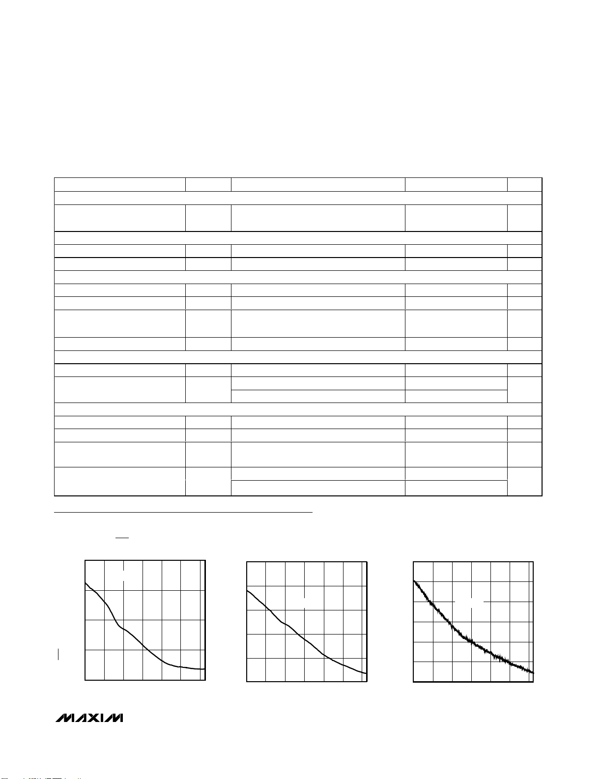
Typical Operating Characteristics
(V+ = 48V, VDD= 13V, CS = GND, NRDV is open circuit, TA= +25°C, unless otherwise noted.)
0.999
1.000
1.001
1.002
1.003
-40 0-20 20 40 60 80
V
SS_SHDN
vs. TEMPERATURE
(AT THE END OF SOFT-START)
MAX5019 toc01
TEMPERATURE (°C)
VFB = 4V
V
SS_SHDN
(V) (NORMALIZED TO V
REF
= 2.4V)
273
274
276
275
277
278
-40 0-20 20 40 60 80
NDRV FREQUENCY
vs. TEMPERATURE
MAX5019 toc02
TEMPERATURE (°C)
NDRV FREQUENCY (kHz)
FB = GND
80.4
80.6
80.5
80.8
80.7
80.9
81.0
-40 20 40-20 0 60 80
MAX5019
MAXIMUM DUTY CYCLE
vs. TEMPERATURE
MAX5019 toc03
TEMPERATURE (°C)
MAXIMUM DUTY CYCLE (%)
FB = GND
SLOPE COMPENSATION
Slope Compensation
(MAX5019 only)
THERMAL SHUTDOWN
Thermal Shutdown Temperature 150 °C
Thermal Hysteresis 25 °C
CURRENT LIMIT
CS Threshold Voltage V
CS Input Bias Current 0 ≤ VCS ≤ 2V, FB = GND -1 1 µA
Current Limit Comparator
Propagation Delay
CS Blanking Time FB = GND, only PWM comparator is blanked 70 ns
OSCILLATOR
Clock Frequency Range FB = GND 247 275 302 kHz
Max Duty Cycle
SOFT-START
SS Source Current I
SS Sink Current 1.0 mA
Steady State Reference Voltage
at SS_SHDN
Shutdown Threshold
PARAMETER SYMBOL CONDITIONS MIN TYP MAX UNITS
V
SCOMP
ILIM
FB = GND 419 465 510 mV
26 mV/µs
50mV overdrive on CS, FB = GND 180 ns
MAX5019, FB = GND 75 85
MAX5020, FB = GND 44 50
SSO
V
_SHDN No external load 2.331 2.420 2.500 V
SS
V
SS_SHDN
V
SS_SHDN
V
SS_SHDN
= 0 2.0 4.5 6.5 µA
falling 0.25 0.37 0.41
rising 0.53 0.59 0.65
%
V
Page 4
MAX5019/MAX5020
Current-Mode PWM Controllers with Integrated
Startup Circuit
4 _______________________________________________________________________________________
Typical Operating Characteristics (continued)
(V+ = 48V, VDD= 13V, CS = GND, NRDV is open circuit, TA= +25°C, unless otherwise noted.)
MAX5020
MAXIMUM DUTY CYCLE
vs. TEMPERATURE
48.0
47.8
47.6
47.4
47.2
MAXIMUM DUTY CYCLE (%)
47.0
46.8
-40 20 40-20 0 60 80
FB = GND
TEMPERATURE (°C)
MAX5019 toc04
V+ SUPPLY CURRENT
vs. TEMPERATURE
1.64
1.63
1.62
1.61
1.60
1.59
1.58
V+ SUPPLY CURRENT (mA)
1.57
1.56
1.55
-40 0 20-20
FB = VDD = GND
TEMPERATURE (°C)
MAX5019 toc05
SOFT-START SOURCE CURRENT (µA)
60 80
40
SOFT-START SOURCE CURRENT
vs. TEMPERATURE
4.50
4.49
4.48
4.47
4.46
4.45
4.44
4.43
4.42
4.41
4.40
-40 -20 0 20 40 60 80
VDD = FB = SS_SHDN = GND
V+ = 110V
TEMPERATURE (°C)
MAX5019 toc06
V+ INPUT CURRENT vs.
TEMPERATURE (AFTER STARTUP)
13.80
13.75
V+ = 110V, VDD = 13V, FB = GND
-40 0-20 20 40 60 80
TEMPERATURE (°C)
V+ INPUT CURRENT (µA)
13.70
13.65
13.60
13.55
13.50
NDRV RESISTANCE
vs. TEMPERATURE
5.0
4.5
NDRV RESISTANCE (Ω)
4.0
3.5
3.0
2.5
2.0
1.5
1.0
-40 0 20-20
HIGH-SIDE DRIVER
LOW-SIDE DRIVER
TEMPERATURE (°C)
MAX5019 toc07
V+ SHUTDOWN CURRENT
vs. TEMPERATURE
182.5
V+ SHUTDOWN CURRENT (µA)
182.0
181.5
181.0
180.5
180.0
179.5
179.0
V+ = 110V, FB = SS_SHDN = GND
-40 -20 0 20 40 60 80
TEMPERATURE (°C)
0.488
MAX5019 toc08
0.487
0.486
0.485
CS THRESHOLD VOLTAGE (V)
0.484
0.483
CS THRESHOLD VOLTAGE
vs. TEMPERATURE
MAX5019 toc09
FB = GND
-40 0-20 20 40 60 80
TEMPERATURE (°C)
CURRENT-LIMIT DELAY
V
vs. TEMPERATURE
MAX5019 toc11
2.410
2.408
(V)
2.406
SS_SHDN
V
2.404
2.402
2.400
010155 2025303540
210
208
MAX5019 toc10
206
FB = GND, 100mV OVERDRIVE ON CS
204
202
200
198
196
194
CURRENT-LIMIT DELAY (ns)
192
190
60 80
40
188
-40 -20 0 20 40 60 80
TEMPERATURE (°C)
SS_SHDN
VDD (V)
vs. V
DD
MAX5019 toc12
Page 5
_______________________________________________________________________________________ 5
MAX5019/MAX5020
Current-Mode PWM Controllers with Integrated
Startup Circuit
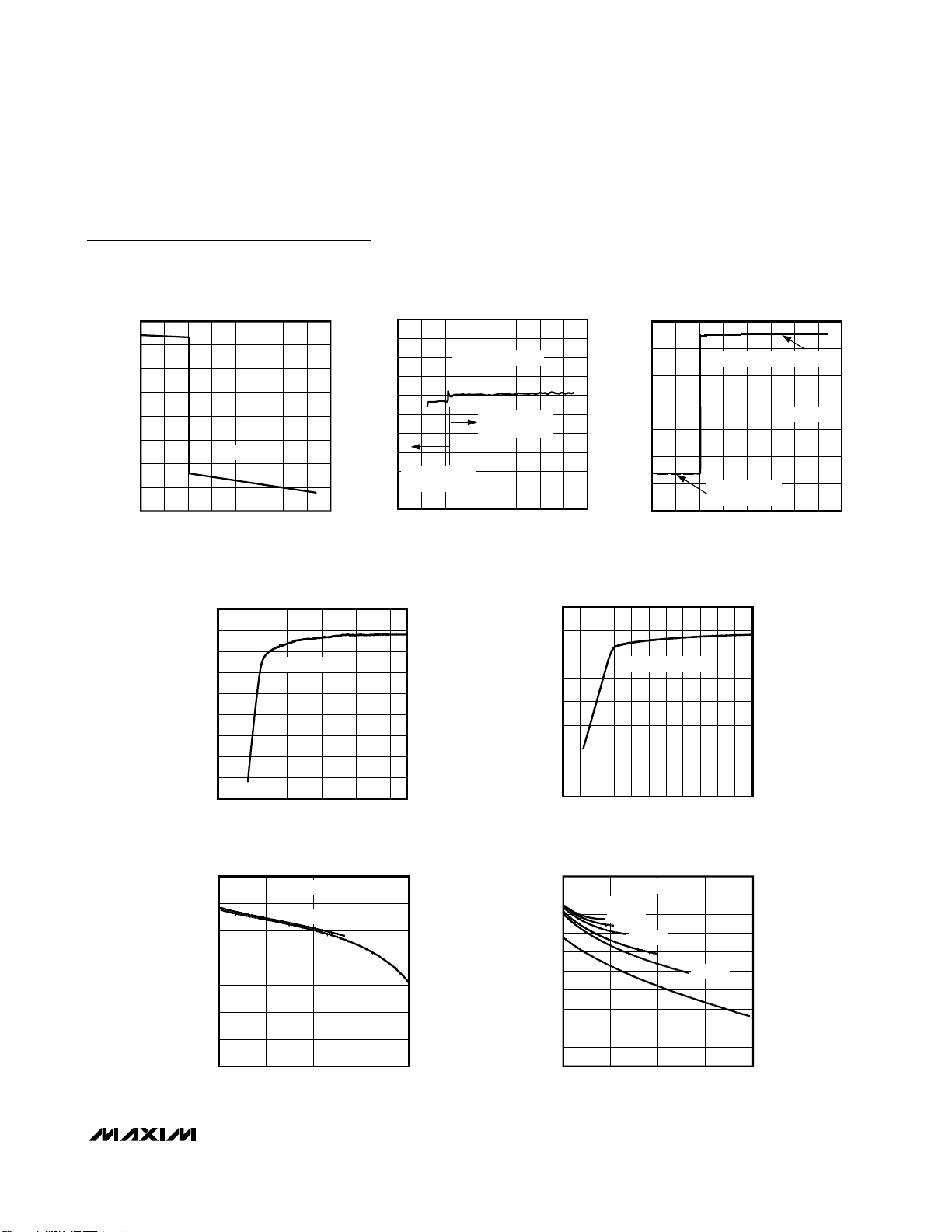
Typical Operating Characteristics (continued)
(V+ = 48V, VDD= 13V, CS = GND, NRDV is open circuit, TA= +25°C, unless otherwise noted.)
267.0
268.0
267.5
269.0
268.5
269.5
270.0
270.5
271.0
010155 2025303540
NDRV FREQUENCY vs. V
DD
MAX5019 toc13
VDD (V)
NDRV FREQUENCY (kHz)
FB = GND
47.0
47.2
47.1
47.4
47.3
47.6
47.5
47.7
47.9
47.8
48.0
010155 2025303540
MAX5020
MAXIMUM DUTY CYCLE vs. V
DD
MAX5019 toc14
VDD (V)
MAXIMUM DUTY CYCLE (%)
VFB = 4V, CS = GND
DEVICE POWERED
FROM V+
DEVICE POWERED
FROM V
DD
9.5
9.6
9.8
9.7
10.0
10.1
9.9
10.2
010155 2025303540
VCC vs. V
DD
MAX5019 toc15
VDD (V)
V
CC
(V)
DEVICE POWERED FROM V
DD
DEVICE POWERED
FROM V+
FB = GND
1.51
1.53
1.52
1.56
1.55
1.54
1.59
1.58
1.57
1.60
04020 60 80 100
V+ SUPPLY CURRENT vs.
V+ VOLTAGE
MAX5019 toc16
V+ VOLTAGE (V)
V+ SUPPLY CURRENT (mA)
VFB = VDD = GND
0
2
14
6
4
8
10
12
16
0403010 20 50 60 70 80 90 110
V+ SUPPLY CURRENT vs. V+ VOLTAGE
(AFTER STARTUP)
MAX5019 toc17
V+ VOLTAGE (V)
V+ LEAKAGE CURRENT (µA)
100
VDD = 13V, FB = GND
9.0
9.4
9.2
9.8
9.6
10.2
10.0
10.4
VCC VOLTAGE vs. VCC CURRENT
MAX5019 toc18
VCC CURRENT (mA)
V
CC
VOLTAGE (V)
0 5.0 10.0 15.0 20.0
V+ = 110V, VFB = 4V
VDD = 36V
VDD = 13V
9.0
9.3
9.2
9.1
9.4
9.5
9.6
9.7
9.8
9.9
10.0
0 5.0 10.0 15.0 20.0
VCC VOLTAGE vs. VCC CURRENT
MAX5019 toc19
VCC CURRENT (mA)
V
CC
VOLTAGE (V)
VDD = GND, VFB = 4V
V+ = 110V
V+ = 90V
V+ = 72V
V+ = 48V
V+ = 36V
V+ = 24V
Page 6

MAX5019/MAX5020
Detailed Description
Use the MAX5019/MAX5020 PWM current-mode controllers to design flyback- or forward-mode power supplies. Current-mode operation simplifies control-loop
design while enhancing loop stability. An internal highvoltage startup regulator allows the device to connect
directly to the input supply without an external startup
resistor. Current from the internal regulator starts the
controller. Once the tertiary winding voltage is established the internal regulator is switched off and bias
current for running the IC is derived from the tertiary
winding. The internal oscillator is set to 275kHz and
trimmed to ±10%. This permits the use of small magnetic components to minimize board space. Both the
MAX5019 and MAX5020 can be used in power supplies providing multiple output voltages. A functional
diagram of the IC is shown in Figure 1. Typical applications circuits for forward and flyback topologies are
shown in Figure 2 and Figure 3, respectively. For isolated flyback power supplies use the circuit of Figure 4.
Current-Mode Control
The MAX5019/MAX5020 offer current-mode control
operation with added features such as leading-edge
blanking with dual internal path that only blanks the
sensed current signal applied to the input of the PWM
comparator. The current limit comparator monitors the
CS pin at all times and provides cycle-by-cycle current
limit without being blanked. The leading-edge blanking
of the CS signal prevents the PWM comparator from
prematurely terminating the on cycle. The CS signal
contains a leading-edge spike that is the result of the
MOSFET gate charge current, capacitive and diode
reverse recovery current of the power circuit. Since this
leading-edge spike is normally lower than the current
limit comparator threshold, current limiting is not
blanked and cycle-by-cycle current limiting is provided
under all conditions.
Use the MAX5019 in discontinuous flyback applications
where wide line voltage and load current variation is
expected. Use the MAX5020 for single transistor forward converters where the maximum duty cycle must
be limited to less than 50%.
Under certain conditions it may be advantageous to
use a forward converter with greater than 50% duty
cycle. For those cases use the MAX5019. The large
duty cycle results in much lower operating primary
RMS currents through the MOSFET switch and in most
cases a smaller output filter inductor. The major disad-
Current-Mode PWM Controllers with Integrated
Startup Circuit
6 _______________________________________________________________________________________
Pin Description
PIN NAME FUNCTION
1V+
2V
3FB
4 SS_SHDN
DD
High-Voltage Startup Input. Connect directly to an input voltage between 18V to 110V. Connects
internally to a high-voltage linear regulator that generates V
VDD is the Input of the Linear Regulator that Generates VCC. For supply voltages less than 36V, V
and V+ can both be connected to the supply. For supply voltages greater than 36V, VDD receives
its power from the tertiary winding of the transformer and accepts voltages from 13V to 36V. Bypass
to GND with a 4.7µF capacitor.
Input of the Fixed-Gain Inverting Amplifier. Connect a voltage-divider from the regulated output to
this pin. The noninverting input of the amplifier is referenced to 2.4V.
Soft-Start Timing Capacitor Connection. Ramp time to full current limit is approximately 0.45ms/nF.
This pin is also the reference voltage output. Bypass with a minimum 10nF capacitor to GND. The
device goes into shutdown when SS_SHDN is pulled below 0.25V.
during startup.
CC
DD
Current Sense Input. Turns power switch off if V
5CS
6 GND Ground
7 NDRV Gate Drive. Drives a high-voltage external N-channel power MOSFET.
8V
CC
limiting. CS is also the feedback for the current-mode controller. CS is connected to the PWM
comparator through a leading-edge blanking circuit.
Regulated IC Supply. Provides power for the entire IC. V
operation and from V+ during startup. Bypass V
0.1µF ceramic capacitor to GND.
rises above 465mV for cycle-by-cycle current
CS
is regulated from VDD during normal
CC
with a 10µF tantalum capacitor in parallel with
CC
Page 7

MAX5019/MAX5020
Current-Mode PWM Controllers with Integrated
Startup Circuit
_______________________________________________________________________________________ 7
Figure 1. Functional Diagram
V
DD
V
DD-OK
V+
GND
IN
EN
HIGH-
VOLTAGE
REGULATOR
OUT
EN
BIAS
WINDING
REGULATOR
OUT
IN
0.7V
V
CC
FB
SS_SHDN
50kΩ
MAX5019 ONLY
26mV/µs
1MΩ
ERROR
AMP
2.4V
SLOPE
COMPENSATION
26mV/µs
∑
DUTY CYCLE
PWM
OSCILLATOR
80%/50%
CLAMP
275kHz
4µA
BUF
UVLO
6.6V
R
Q
S
ILIM
V
CC
70ns
BLANKING
3R
125mV
5kΩ
R
V
CC
NDRV
CS
0.25V
Page 8

MAX5019/MAX5020
vantage to this is that the MOSFET voltage rating must
be higher and that slope compensation must be provided to stabilize the inner current loop. The MAX5019
provides internal slope compensation.
Internal Regulators
The internal regulators of the MAX5019/MAX5020
enable initial startup without a lossy startup resistor and
regulate the voltage at the output of a tertiary (bias)
winding to provide power for the IC. At startup V+ is
regulated down to VCCto provide bias for the device.
The VDDregulator then regulates from the output of the
tertiary winding to VCC. This architecture allows the tertiary winding to only have a small filter capacitor at its
output thus eliminating the additional cost of a filter
inductor.
When designing the tertiary winding calculate the number of turns so the minimum reflected voltage is always
higher than 12.7V. The maximum reflected voltage
must be less than 36V.
To reduce power dissipation the high-voltage regulator
is disabled when the VDDvoltage reaches 12.7V. This
greatly reduces power dissipation and improves efficiency. If VCCfalls below the undervoltage lockout
threshold (VCC= 6.6V), the low-voltage regulator is dis-
abled, and soft-start is reinitiated. In undervoltage lockout the MOSFET driver output (NDRV) is held low.
If the input voltage range is between 13V and 36V, V+
and VDDmay be connected to the line voltage provided that the maximum power dissipation is not exceeded. This eliminates the need for a tertiary winding.
Undervoltage Lockout (UVLO), Soft-Start,
and Shutdown
The soft-start feature of the MAX5019/MAX5020 allows
the load voltage to ramp up in a controlled manner,
thus eliminating output voltage overshoot.
While the part is in UVLO, the capacitor connected to
the SS_SHDN pin is discharged. Upon coming out of
UVLO an internal current source starts charging the
capacitor to initiate the soft-start cycle. Use the following equation to calculate total soft-start time:
where CSSis the soft-start capacitor as shown in Figure 2.
Operation begins when V
SS_SHDN
ramps above 0.6V.
When soft-start has completed, V
SS_SHDN
is regulated
Current-Mode PWM Controllers with Integrated
Startup Circuit
8 _______________________________________________________________________________________
Figure 2. Forward Converter
1N4148
V
IN
(36V TO 72V)
V
C
4.7µF
C
10µF
C
0.1µF
DD
CC
SS
DD
V
CC
SS_SHDN
6
MAX5020
N
T
NDRV
GND
V+
CS
FB
N
R
14
CMHD2003
C
3
0.47µF
IRF640N
IN
✕
M1
100Ω
N
P
14 5
R
SENSE
100mΩ
N
S
SBL204OCT
20Ω
1nF
C
FB
(OPTIONAL)
L1
4.7µH
R
2kΩ
R
2kΩ
1
2
5V/10A
C
OUT
✕
3
560µF
V
OUT
0.1µF
=×045.
ms
nF
C
t
startup ss
Page 9

to 2.4V, the internal voltage reference. Pull V
SS_SHDN
below 0.25V to disable the controller.
Undervoltage lockout shuts down the controller when
VCCis less than 6.6V. The regulators for V+ and the reference remain on during shutdown.
Current-Sense Comparator
The current-sense (CS) comparator and its associated
logic limit the peak current through the MOSFET.
Current is sensed at CS as a voltage across a sense
resistor between the source of the MOSFET and GND.
To reduce switching noise, connect CS to the external
MOSFET source through a 100Ω resistor or an RC low-
_______________________________________________________________________________________ 9
MAX5019/MAX5020
Current-Mode PWM Controllers with Integrated
Startup Circuit
Figure 3. Nonisolated Flyback Converter
Figure 4. Isolated Flyback Converter
N
V
IN
T
C
V
C
DD
C
CC
C
SS
DD
V
CC
SS_SHDN
MAX5019
MAX5020
V+
NDRV
CS
GND
FB
IN
M1
100Ω
N
N
P
S
R
SENSE
V
OUT
C
OUT
R
1
R
2
V
IN
V
C
DD
R
1
R
2
C
CC
C
SS
DD
FB
V
CC
SS_SHDN
MAX5019
MAX5020
N
NDRV
GND
T
C
V+
CS
IN
M1
100Ω
N
N
P
S
R
SENSE
V
OUT
C
OUT
Page 10

MAX5019/MAX5020
pass filter (Figures 2, 3). Select the current-sense resistor, R
SENSE
according to the following equation:
where I
LimPrimary
is the maximum peak primary-side
current.
When VCS> 465mV, the power MOSFET switches off.
The propagation delay from the time the switch current
reaches the trip level to the driver turn-off time is 180ns.
Internal Error Amplifier
The MAX5019/MAX5020 include an internal error amplifier that can be used to regulate the output voltage in
the case of a nonisolated power supply (see Figure 2).
Calculate the output voltage using the following equation:
where V
REF
= 2.4V.
Choose R1//R2<< RIN, where RIN, ≅ 50kΩ is the input
resistance of FB. The gain of the error amplifier is internally configured for -20 (see Figure 1).
The error amplifier may also be used to regulate the output of the tertiary winding for implementing a primaryside regulated isolated power supply (see Figure 4).
Calculate the output voltage using the following equation:
where NSis the number of secondary turns and NTis
the number of tertiary winding turns.
PWM Comparator and Slope Compensation
An internal 275kHz oscillator determines the switching
frequency of the controller. At the beginning of each
cycle, NDRV switches the N-channel MOSFET on.
NDRV switches the external MOSFET off after the maximum duty cycle has been reached, regardless of the
feedback.
The MAX5019 uses an internal ramp generator for
slope compensation. The internal ramp signal is reset
at the beginning of each cycle and slews at 26mV/µs.
The PWM comparator uses the instantaneous current,
the error voltage, the internal reference, and the slope
compensation (MAX5019 only) to determine when to
switch the N-channel MOSFET off. In normal operation
the N-channel MOSFET turns off when:
where I
PRIMARY
is the current through the N-channel
MOSFET, V
REF
is the 2.4V internal reference, VEAis the
output voltage of the internal amplifier, and V
SCOMP
is
a ramp function starting at 0 and slewing at 26mV/µs
(MAX5019 only). When using the MAX5019 in a forward-converter configuration the following condition
must be met to avoid control-loop subharmonic oscillations:
where k = 0.75 to 1, and N
S
and NPare the number of
turns on the secondary and primary side of the transformer, respectively. L is the output filter inductor. This
makes the output inductor current downslope as referenced across R
SENSE
equal to the slope compensation. The controller responds to transients within one
cycle when this condition is met.
N-Channel MOSFET Gate Driver
NDRV drives an N-channel MOSFET. NDRV sources
and sinks large transient currents to charge and discharge the MOSFET gate. To support such switching
transients, bypass VCCwith a ceramic capacitor. The
average current as a result of switching the MOSFET is
the product of the total gate charge and the operating
frequency. It is this current plus the DC quiescent current that determines the total operating current.
Applications Information
Design Example
The following is a general procedure for designing a
forward converter using the MAX5020.
1) Determine the requirements.
2) Set the output voltage.
3) Calculate the transformer primary to secondary
winding turns ratio.
4) Calculate the reset to primary winding turns ratio.
5) Calculate the tertiary to primary winding turns
ratio.
6) Calculate the current-sense resistor value.
7) Calculate the output inductor value.
8) Select the output capacitor.
The circuit in Figure 2 was designed as follows:
Current-Mode PWM Controllers with Integrated
Startup Circuit
10 ______________________________________________________________________________________
RI
= 0 465./V
SENSE LimPrimary
V
OUT
R
=+
R
1
×1
V
REF
2
N
V
OUT
S
=+
N
T
R
1
V
×1
R
REF
2
IRV-V-V
PRIMARY SENSE EA REF SCOMP
×>
NNkR V
××
S
P
×
SENSE OUT
L
=µ
mV s26 /
Page 11

1) 36V ≤ VIN≤ 72V, V
OUT
= 5V, I
OUT
= 10A, V
RIPPLE
≤
50mV
2) To set the output voltage calculate the values of
resistors R1 and R2 according to the following
equation:
where V
REF
is the reference voltage of the shunt
regulator, and R1and R2are the resistors shown in
Figures 2 and 3.
3) The turns ratio of the transformer is calculated based
on the minimum input voltage and the lower limit of
the maximum duty cycle for the MAX5020 (44%). To
enable the use of MOSFETs with drain-source
breakdown voltages of less than 200V use the
MAX5020 with the 50% maximum duty cycle.
Calculate the turns ratio according to the following
equation:
where:
NS/NP= Turns ratio (NSis the number of secondary
turns and NPis the number of primary turns).
V
OUT
= Output voltage (5V).
VD1= Voltage drop across D1 (typically 0.5V for
power Schottky diodes).
D
MAX
= Minimum value of maximum operating duty
cycle (44%).
V
IN_MIN
= Minimum Input voltage (36V).
In this example:
Choose NPbased on core losses and DC resistance. Use the turns ratio to calculate NS, rounding
up to the nearest integer. In this example NP= 14
and NS= 5.
For a forward converter choose a transformer with a
magnetizing inductance in the neighborhood of
200µH. Energy stored in the magnetizing inductance
of a forward converter is not delivered to the load
and must be returned back to the input; this is
accomplished with the reset winding.
The transformer primary to secondary leakage
inductance should be less than 1µH. Note that all
leakage energy will be dissipated across the MOSFET. Snubber circuits may be used to direct some or
all of the leakage energy to be dissipated across a
resistor.
To calculate the minimum duty cycle (D
MIN
) use the
following equation:
where V
IN_MAX
is the maximum input voltage (72V).
4) The reset winding turns ratio (NR/NP) needs to be
low enough to guarantee that the entire energy in
the transformer is returned to V+ within the off cycle
at the maximum duty cycle. Use the following equation to determine the reset winding turns ratio:
where:
NR/NP= Reset winding turns ratio.
D
MAX
’ = Maximum value of Maximum Duty Cycle.
Round N
R
to the nearest smallest integer.
The turns ratio of the reset winding (NR/NP) will
determine the peak voltage across the N-channel
MOSFET.
Use the following equation to determine the maximum drain-source voltage across the N-channel
MOSFET:
V
DSMAX
= Maximum MOSFET drain-source voltage.
V
IN_MAX
= Maximum input voltage.
MAX5019/MAX5020
Current-Mode PWM Controllers with Integrated
Startup Circuit
______________________________________________________________________________________ 11
VV
OUT REF
RR k//
12
VV V
REF SS_
≅+
<<
50
=≅
SHDN
R
1
1
R
2
Ω
24
.
VVD
+×
N
S
≥
N
P
()
OUT D1 MAX
×
DV
MAX IN_MIN
5V+ 0.5V 0.44
N
S
≥
N
P
×
()
×
044 36
=
V
0 330..
D
=
MIN
V
IN_MAX
V
OUT
×
N
S
-V
D1
N
P
NN
≤×
RP
1-D
D
MAX
MAX
′
′
1- 0.5
≤× =414
0.5
N1
R
VV 1 +
≥×
DSMAX IN_MAX
N
P
N
R
Page 12

MAX5019/MAX5020
Choose MOSFETs with appropriate avalanche
power ratings.
5) Choose the tertiary winding turns ratio (NT/NP) so
that the minimum input voltage provides the minimum operating voltage at V
DD
(13V). Use the following equation to calculate the tertiary winding turns
ratio:
where:
V
DDMIN
is the minimum VDDsupply voltage (13V).
V
DDMAX
is the maximum VDDsupply voltage (36V).
V
IN_MIN
is the minimum input supply voltage (36V).
V
IN_MAX
is the maximum input supply voltage (72V
in this design example).
NPis the number of turns of the primary winding.
NTis the number of turns of the tertiary winding.
Choose NT= 6.
6) Choose R
SENSE
according to the following equation:
where:
V
ILim
is the current-sense comparator trip threshold
voltage (0.465V).
NS/NPis the secondary side turns ratio (5/14 in this
example).
I
OUTMAX
is the maximum DC output current (10A in
this example).
7) Choose the inductor value so that the peak ripple
current (LIR) in the inductor is between 10% and
20% of the maximum output current.
where V
D
is the output Schottky diode forward volt-
age drop (0.5V).
8) The size and ESR of the output filter capacitor determine the output ripple. Choose a capacitor with a
low ESR to yield the required ripple voltage.
Use the following equations to calculate the peak-topeak output ripple:
where:
V
RIPPLE
is the combined RMS output ripple due to
VRIPPLE,ESR, the ESR ripple, and V
RIPPLE,C
, the
capacitive ripple. Calculate the ESR ripple and
capacitive ripple as follows:
V
RIPPLE,ESR
= I
RIPPLE
x ESR
V
RIPPLE,C
= I
RIPPLE
/(2 x π x 275kHz x C
OUT
)
Layout Recommendations
All connections carrying pulsed currents must be very
short, be as wide as possible, and have a ground plane
as a return path. The inductance of these connections
must be kept to a minimum due to the high di/dt of the
currents in high-frequency switching power converters.
Current loops must be analyzed in any layout proposed, and the internal area kept to a minimum to
reduce radiated EMI. Ground planes must be kept as
intact as possible.
Chip Information
TRANSISTOR COUNT: 589
PROCESS: BiCMOS
Current-Mode PWM Controllers with Integrated
Startup Circuit
12 ______________________________________________________________________________________
14
V71 +
DSMAX
≥×
=2 144VV
14
V
IN_MIN
V
IN_MAX
0707.
+
×≤≤
+
.
×
NN
PT
N
P
V
DDMIN
V
DDMAX
13 7
..
4
1N
×≤ ≤ ×
36
533 714
..
N
≤≤
36 7
72
14
T
V
R
SENSE
≤
N
N
ILIM
S
××12.I
P
OUTMAX
0 465
R
SENSE
≤
14
..V
5
××
12 10
=Ω
109
m
VD
×
1
()
DMIN
OUTMAX
V-
+
()
L
OUT
≥
×× ×
LIR kHz I
2 275
×
5 5 1 0 198
..
()
L-≥
0 4 275 10
()
××
.
kHz A
=µ
401
.
H
VV V
RIPPLE RIPPLEESR RIPPLE C
22
=+
,,
Page 13

MAX5019/MAX5020
Current-Mode PWM Controllers with Integrated
Startup Circuit
______________________________________________________________________________________ 13
Table 1. Component Manufacturers
Selector Guide
International Rectifier www.irf.com
Power FETS
Current-Sense Resistors
Capacitors
Fairchild www.fairchildsemi.com
Vishay-Siliconix www.vishay.com/brands/siliconix/main.html
Dale-Vishay www.vishay.com/brands/dale/main.html
IRC www.irctt.com/pages/index.cfm
On Semi www.onsemi.com
General Semiconductor www.gensemi.comDiodes
Central Semiconductor www.centralsemi.com
Sanyo www.sanyo.com
Taiyo Yuden www.t-yuden.com
AVX www.avxcorp.com
Coiltronics www.cooperet.com
Coilcraft www.coilcraft.comMagnetics
Pulse Engineering www.pulseeng.com
PART
MAX5019CSA 85% Yes
MAX5019ESA 85% Yes
MAX5020CSA 50% No
MAX5020ESA 50% No
MAXIMUM
DUTY CYCLE
SLOPE
COMPENSATION
Page 14

MAX5019/MAX5020
Current-Mode PWM Controllers with Integrated
Startup Circuit
Maxim cannot assume responsibility for use of any circuitry other than circuitry entirely embodied in a Maxim product. No circuit patent licenses are
implied. Maxim reserves the right to change the circuitry and specifications without notice at any time.
14 ____________________Maxim Integrated Products, 120 San Gabriel Drive, Sunnyvale, CA 94086 408-737-7600
© 2001 Maxim Integrated Products Printed USA is a registered trademark of Maxim Integrated Products.
Package Information
SOICN.EPS
 Loading...