_______________General Description
The MAX5018 is a monolithic, 8-bit digital-to-analog
converter (DAC) capable of accepting video data at
165Msps or 275Msps. Complete with video controls
(sync, blank, reference white (force high), and bright),
the MAX5018 directly drives doubly terminated 50Ω or
75Ω loads to standard composite video levels.
Standard setup level is 7.5IRE. The MAX5018 is pin
compatible with the HDAC10180 and the TDC1018,
with improved performance. The MAX5018 contains
data and control input registers, video control logic, reference buffer, and current switches.
Two performance grades of the MAX5018 are available.
Both are packaged in a 24-pin PDIP in the -20°C to
+85°C industrial temperature range.
________________________Applications
High-Resolution Color or Monochrome Raster
Graphics Displays to 1500 x 1800 Pixels
Medical Electronics: CAT, PET, and MRI Displays
CAD/CAE Workstations
Solids Modeling
General-Purpose, High-Speed Digital-to-Analog
Conversion
Digital Synthesizers
Automated Test Equipment
Digital Transmitters/Modulators
____________________________Features
♦ 275Msps Conversion Rate (MAX5018A)
165Msps Conversion Rate (MAX5018B)
♦ TDC1018 and HDAC10180 Compatible with
Improved Performance
♦ RS-343-A Compatible
♦ Complete Video Controls: Sync, Blank, Bright,
and Reference White (force high)
♦ ECL Compatible
♦ Single Power Supply
♦ Registered Data and Video Controls
♦ Differential Current Outputs
♦ ESD-Protected Data and Control Inputs
MAX5018
8-Bit, High-Speed DAC
________________________________________________________________
Maxim Integrated Products
1
19-1204; Rev 0; 3/97
For the latest literature: http://www.maxim-ic.com, or phone 1-800-998-8800
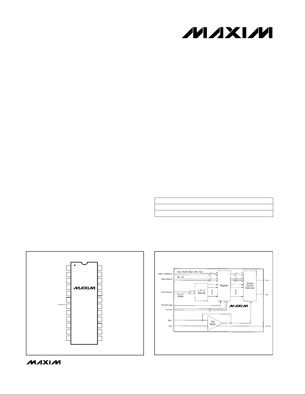
__________________Pin Configuration
24
23
22
21
20
19
18
17
1
2
3
4
5
6
7
8
D4
D5
D6
D7D0
D1
D2
D3
TOP VIEW
V
EE
Out+
OutV
CC
FT
CONV
CONV
V
EE
16
15
14
13
9
10
11
12
COMP
Ref+
RefSyncBRT
Blank
FH
V
CC
DIP
MAX5018
________________Functional Diagram
______________Ordering Information
PART
MAX5018BIPG
MAX5018AIPG
-20°C to +85°C 24 Plastic DIP
-20°C to +85°C
TEMP. RANGE PIN-PACKAGE
24 Plastic DIP
MAX5018

MAX5018
8-Bit, High-Speed DAC
2 _______________________________________________________________________________________
ABSOLUTE MAXIMUM RATINGS
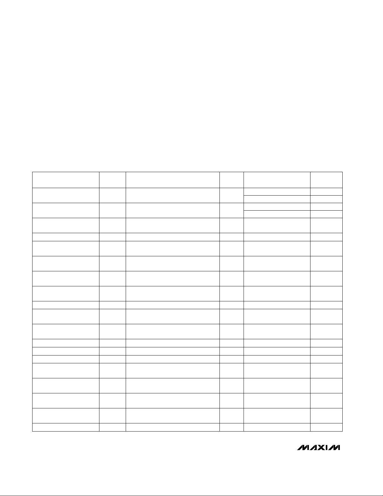
DC ELECTRICAL CHARACTERISTICS
(VCC= ground, VEE= -5.2V ±0.3V, CC= 0pF, I
SET
= 1.105mA, TA= T
MIN
to T
MAX
, unless otherwise noted.)
Stresses beyond those listed under “Absolute Maximum Ratings” may cause permanent damage to the device. These are stress ratings only, and functional
operation of the device at these or any other conditions beyond those indicated in the operational sections of the specifications is not implied. Exposure to
absolute maximum rating conditions for extended periods may affect device reliability.
Supply Voltage
V
EE
(measured to VCC)..........................................-7.0V to 0.5V
Input Voltages
CONV, Data, and Controls (measured to V
CC
)........VEEto 0.5V
Ref+ (measured to V
CC
) ..........................................VEEto 0.5V
Ref- (measured to V
CC
)............................................VEEto 0.5V
Operating Temperature Ranges
Ambient .............................................................-20°C to +85°C
Junction..........................................................................+175°C
Lead Temperature (soldering, 10sec).............................+300°C
Storage Temperature Range.............................-60°C to +150°C
µA35 120I
IL
Input Current, Logic Low,
Data and Controls
-0.95 0.95
VI
-0.5 0.5
CONDITIONS
µA40 120I
IH
Input Current, Logic High,
Data and Controls
VI
µA2 60I
CONV
Input Current, Convert VI
1.0mA < I
SET
< 1.3mA
% Full Scale-0.37 0.37
ILEIntegral Linearity Error VI
1.0mA < I
SET
< 1.3mA
% Full Scale-0.2 0.2
DLEDifferential Linearity Error
V0.4 1.2
Convert Voltage,
Differential
V-0.5 -2.5
Convert Voltage,
Common-Mode Range
V-1.5V
IL
Input Voltage, Logic Low
V-1.0V
IH
Input Voltage, Logic High
LSB0.05 0.5I
OS
Output Offset Current
mA-45IO-
(MAX)
Maximum Current,
Negative Output
% Full Scale-6.5 6.5Gain Error
mA45IO+
(MAX)
Maximum Current,
Positive Output
pF12C
OUT
Output Capacitance
kΩ20R
OUT
Equivalent Output
Resistance
V-1.2 1.5
Compliance Voltage,
Negative Output
ppm/°C150Gain-Error Tempco
pF5C
REF
Input Capacitance,
Ref+, Ref-
V-1.2 1.5
Compliance Voltage,
Positive Output
UNITSMIN TYP MAXSYMBOLPARAMETER
VI
VI
IV
IV
IV
V
VI
VI
VI
VI
V
V
VI
VI
IV
TEST
LEVEL
LSB
LSB

Msps
MAX5018
8-Bit, High-Speed DAC
_______________________________________________________________________________________ 3
To 0.2% G.S., RL= 25Ω 4.5
MAX5018B
V
MAX5018A 275
t
S
III
10% to 90% G.S., RL= 25Ω 1.0
2.0
IV
V
CONDITIONS
10% to 90% G.S., TA= T
MIN
to T
MAX
ns
1.6
t
R
Rise Time
III
To 0.8% G.S. 5.5V
IV
TA= T
MIN
to T
MAX
4.5
t
H
TA= T
MIN
to T
MAX
ns
2.2 4.0
t
DSC
Clock to Output Delay,
Clocked Mode
III
IV
To 0.2% G.S. 7.0V
TA= T
MIN
to T
MAX
ns
6.0
t
DST
IV
Area = 1/2VT pV-s
Msps
165
Maximum Conversion Rate
4
A Grade 1.8
Glitch Energy
Convert Pulse Width,
(low or high)
V
B Grade
ns
3.0
t
PWL
,
t
PWH
III
TA= +25°C
ns
1.0
MHz1.0Reference Bandwidth, -3dB V
TA= T
MIN
to T
MAX
ns
0.5IV
TA= +25°C 0.5
Hold Time, Data and
Controls
III
III
UNITSMIN TYP MAXSYMBOLPARAMETER
1.0
III
Setup Time, Data and
Controls
III
3.2 6.0
Data to Output Delay,
Transparent Mode
III
dB
-48
Clock Feedthrough
III
TA= T
MIN
to T
MAX
325IV
TEST
LEVEL
TA= T
MIN
to T
MAX
-48IV
20% to 80% G.S., TA= +25°C
V/µs
390
Slew Rate
III
CONDITIONS
mA155 220I
EE
Supply Current
pF3C
IN
Input Capacitance, Data
and Controls
µA/V-120 20 120Power-Supply Sensitivity
UNITSMIN TYP MAXSYMBOLPARAMETER
VI
V
VI
TEST
LEVEL
DC ELECTRICAL CHARACTERISTICS (continued)
(VCC= ground, VEE= -5.2V ±0.3V, CC= 0pF, I
SET
= 1.105mA, TA= T
MIN
to T
MAX
, unless otherwise noted.)
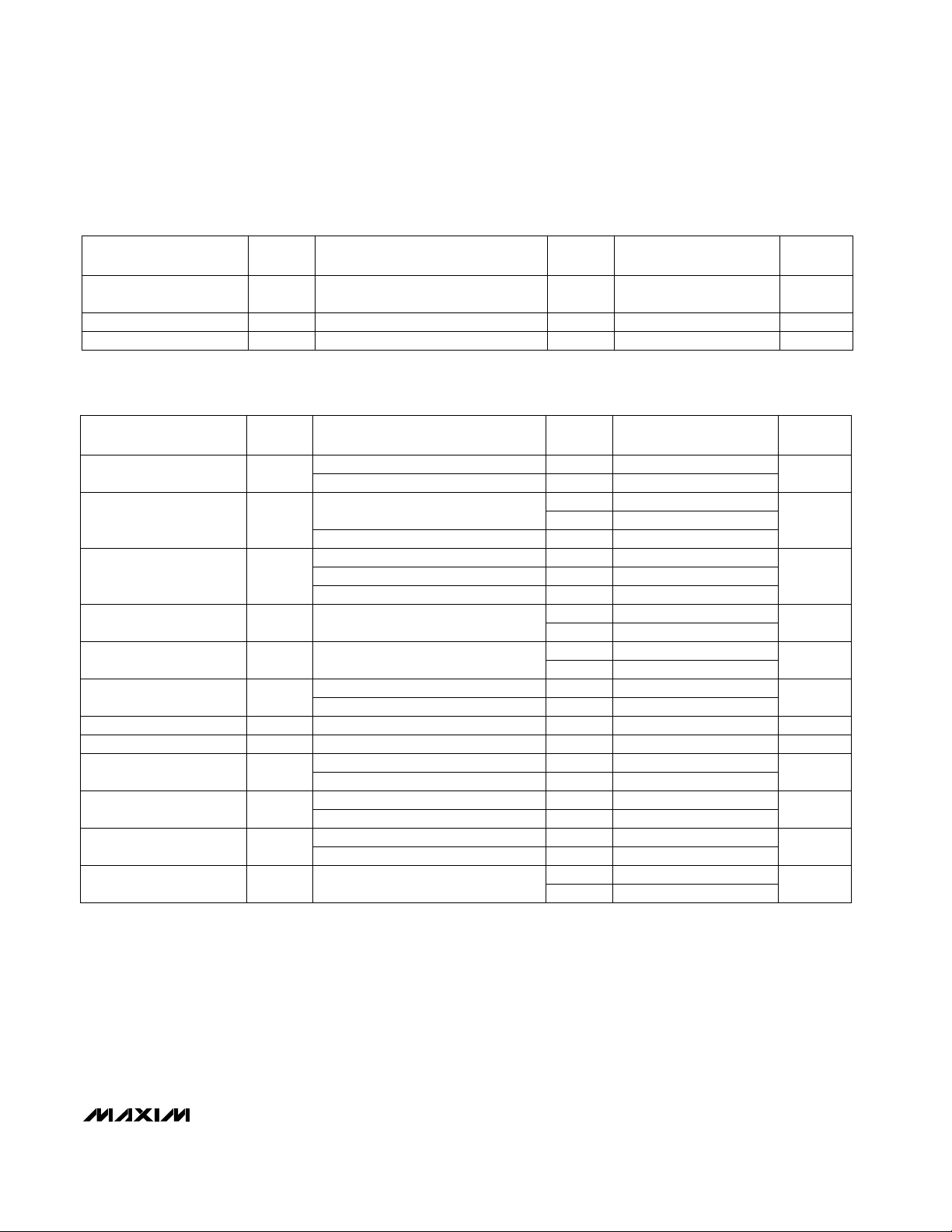
AC ELECTRICAL CHARACTERISTICS
(RL= 37.5Ω, CL= 5pF, I
SET
= 1.105mA, TA= +25°C, unless otherwise noted.)
t
SI
ns
Current Settling Time,
Clocked Mode

MAX5018
8-Bit, High-Speed DAC
4 _______________________________________________________________________________________
Data Bit 0 (LSB)D04
Convert Clock InputCONV6
Negative SupplyV
EE
5, 20
Register Feedthrough ControlFT8
Data Force-High ControlFH10
Positive SupplyV
CC
9, 17
Convert-Clock-Input Complement
CONV
7
Video Bright InputBRT12
Reference Current, Negative InputRef-14
Video Sync InputSync13
Compensation InputCOMP16
PIN
Output Current NegativeOut-18
Data Bits 3, 2, and 1D3, D2, D11, 2, 3
FUNCTIONNAME
Reference Current, Positive InputRef+15
Video Blank InputBlank11
Data Bits 6, 5, and 4D6, D5, D422, 23, 24
Data Bit 7 (MSB)D721
Output Current PositiveOut+19
______________________________________________________________Pin Description
TEST-LEVEL CODES
All electrical characteristics are subject to
the following conditions:
All parameters having min/max specifications are guaranteed. The Test Level column
indicates the specific device testing actually
performed during production and Quality
Assurance inspection. Any blank section in
the data column indicates that the specification is not tested at the specified condition.
Unless otherwise noted, all tests are pulsed
tests; therefore, T
j
= TC= TA.
TEST LEVEL
I
II
III
IV
V
VI
TEST PROCEDURE
100% production tested at the specified temperature.
100% production tested at T
A
= +25°C, and sample
tested at the specified temperatures.
QA sample tested at only the specified temperatures.
Parameter is guaranteed (but not tested) by design
and characterization data.
Parameter is a typical value for reference only.
100% production tested at T
A
= +25°C. Parameter is
guaranteed over specified temperature range.
 Loading...