

Page 1
现货库存、技术资料、百科信息、热点资讯,精彩尽在鼎好!
General Description
The MAX5008 charge-pump regulator generates a regulated 5V output up to 125mA with a 2.95V to 5.5V input
voltage range. The device includes resistor-programmable overcurrent limit. The MAX5008 requires a minimum number of external components for normal
operation. The high 1MHz switching frequency allows
the use of small surface-mount ceramic capacitors.
The fault-protection circuitry limits the output current
when it exceeds the limit set by an external resistor.
The output current can range from 1mA to 150mA to
accommodate circuit requirements. A FAULT output
indicates when the device is in current limit or the output is out of regulation.
A low-power shutdown mode reduces supply current to
less than 1µA and places the output in a high-impedance state. The MAX5008 is offered in a space-saving
10-pin µMAX package that is only 1.1mm high.
Applications
Flash Memory Supplies
USB Host Devices
Battery-Powered Systems
3.3V to 5V Local Conversion
Features
♦ Regulated 5V Output Up to 125mA
♦ Indefinite Short-Circuit Protection
♦ Adjustable Output Current Limit
♦ No Inductors Required
♦ 0.1µA Shutdown Current
♦ Thermal Shutdown
♦ Fault Output Indicates Overcurrent or Output
Voltage Out of Regulation
♦ 2.95V to 5.5V Input Voltage Range
♦ 10-Pin µMAX Package
MAX5008
Regulated 5V USB Charge Pump with
Programmable Current Limit
________________________________________________________________ Maxim Integrated Products 1
Ordering Information
19-2426; Rev 0; 4/02
For pricing, delivery, and ordering information, please contact Maxim/Dallas Direct! at
1-888-629-4642, or visit Maxim’s website at www.maxim-ic.com.
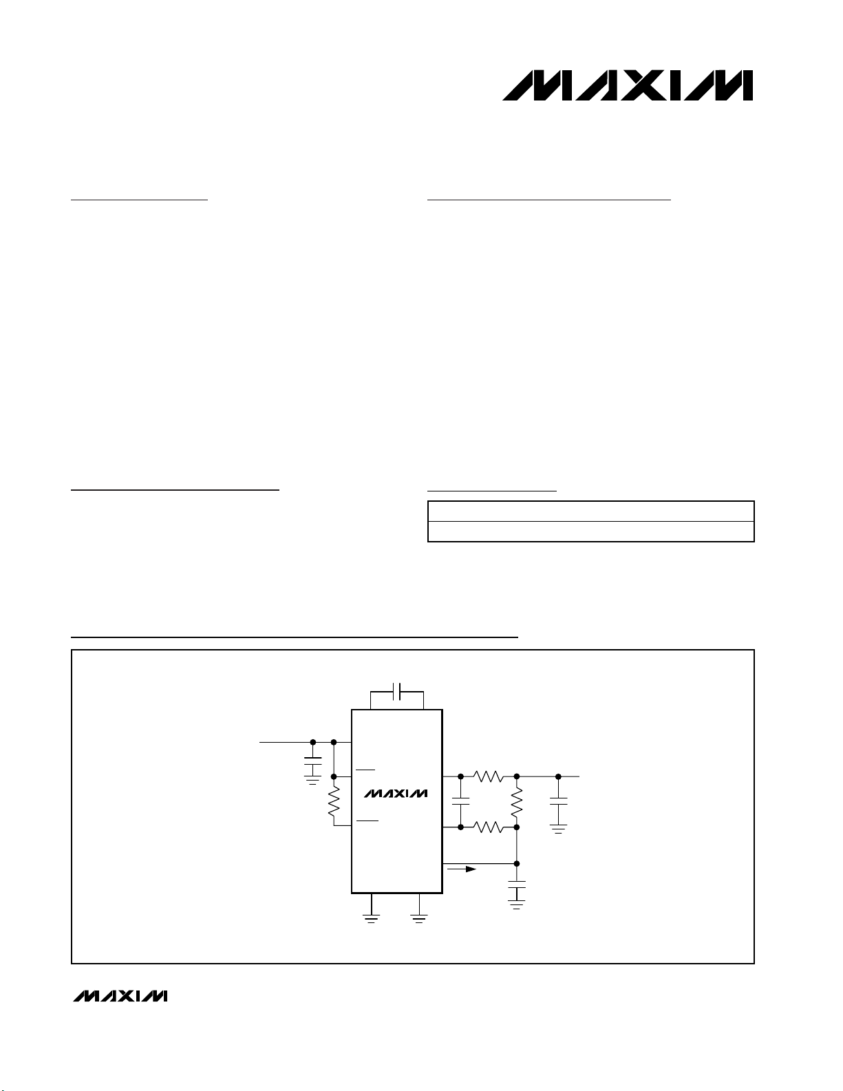
Typical Operating Circuit
Pin Configuration appears at end of data sheet.
PART TEMP RANGE PIN-PACKAGE
MAX5008CUB 0°C to +70°C 10 µMAX
C
X
0.68µF
7
V
IN
2.95V TO 5.5V
4.7µF
100kΩ
*USE IF PRECISION CURRENT LIMIT IS REQUIRED.
CXN
8
IN
5
SHDN
3
FAULT
GND PGND
46
MAX5008
9
CXP
CEXT
OUT
RCS
200Ω*
2
R
47nF*
1
200Ω*
10
I
OUT
CS
0.4Ω
C
6.8µF
EXT
C
OUT
4.7µF
V
OUT
5V
Page 2
MAX5008
Regulated 5V USB Charge Pump with
Programmable Current Limit
2 _______________________________________________________________________________________
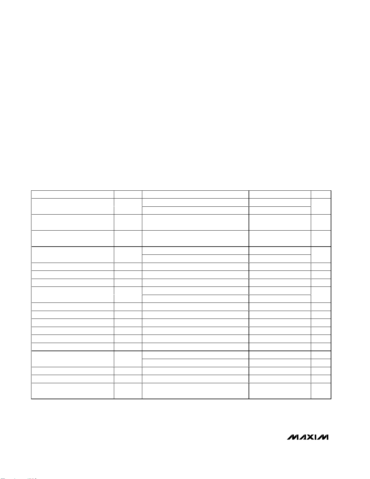
ABSOLUTE MAXIMUM RATINGS
ELECTRICAL CHARACTERISTICS
(VIN= SHDN = 3V, CIN= 4.7µF, CX= 0.68µF, C
EXT
= 6.8µF, C
OUT
= 4.7µF, RCS= 0.4Ω, TA= 0°C to +70°C, unless otherwise noted.
Typical values are at T
A
= +25°C.)
Stresses beyond those listed under “Absolute Maximum Ratings” may cause permanent damage to the device. These are stress ratings only, and functional
operation of the device at these or any other conditions beyond those indicated in the operational sections of the specifications is not implied. Exposure to
absolute maximum rating conditions for extended periods may affect device reliability.
IN, SHDN, RCS, FAULT, OUT to GND .....................-0.3V to +6V
PGND to GND.....................................................................±0.3V
CXN to GND ................................................-0.3V to (V
IN
+ 0.3V)
CXP to GND ............................................-0.3V to (V
CEXT
+ 0.3V)
CEXT to GND ..........................................-0.3V to (V
CEXT
+ 0.3V)
Short-Circuit Duration to GND .......................................Indefinite
Continuous Power Dissipation (T
A
= +70°C)
10-Pin µMAX.................................................................444mW
Operating Temperature Range...............................0°C to +70°C
Junction Temperature......................................................+150°C
Storage Temperature Range .............................-65°C to +150°C
Lead Temperature (soldering, 10s) .................................+300°C
PARAMETER SYMBOL CONDITIONS MIN TYP MAX UNITS
Input Voltage Range
(Note 1)
V
IN
Input Undervoltage Lockout
Threshold
Input Undervoltage Lockout
Hysteresis
Output Voltage
(Note 2)
Output Voltage Ripple V
V
Fault Threshold V
OUT
Maximum Output Current I
No-Load Input Current I
SHDN Logic High V
SHDN Logic Low V
Shutdown Supply Current I
Current-Sense Trip Level V
V
OUT
RIP
TH
OUT
Q
INH,SHDN
INL,SHDN
QSHDN
CS
FAULT Leakage Current V
FAULT Logic Low I
FAULT Assertion Delay
(Note 4)
FAULT Deassertion Delay (Note 5) t
t
FD
FDD
Switching Frequency 0.5 1 1.5 MHz
Startup Time t
START
I
= 125mA 2.95 4.25
OUT
I
= 70mA 2.95 5.50
OUT
Rising edge 2.0 2.35 2.6 V
Falling edge 100 mV
0 ≤ I
0mA ≤ I
0mA ≤ I
V
I
OUT
I
OUT
< 30mA, 2.95V < V
OUT
≤ 100mA, 2.95V ≤ V
OUT
≤ 125mA 100 mV
OUT
= 5V ±4% 100 140 mA
OUT
< 5.5V 4.75 5.0 5.30
IN
≤ 4.25V 4.75 5.0 5.25
IN
= 0, VIN = 4.25V 0.6 6
= 0, VIN = 3.3V 1 6
SHDN = low 0.1 10 µA
V
= I
x R
CS
OUT
= 5V, OUT in regulation 1 µA
FAULT
> I
OUT
LIMIT
I
> I
OUT
LIMIT
< V
V
OUT
TH
I
< I
OUT
LIMIT
V
> VTH, R
OUT
(Note 3) 55 60 73 mV
CS
, or V
and V
< VTH, I
OUT
OUT
= 46Ω, from rising edge
LOAD
FAULT
> 4.5V 16 ms
= 1mA 0.4 V
of SHDN
4.22 4.50 V
2.4 V
0.4 V
2ms
30 µs
200 µs
V
V
mA
Page 3
MAX5008
Regulated 5V USB Charge Pump with
Programmable Current Limit
_______________________________________________________________________________________ 3
ELECTRICAL CHARACTERISTICS (continued)
(VIN= SHDN = 3V, CIN= 4.7µF, CX= 0.68µF, C
EXT
= 6.8µF, C
OUT
= 4.7µF, RCS= 0.4Ω, TA= 0°C to +70°C, unless otherwise noted.
Typical values are at T
A
= +25°C.)
Note 1: When the input exceeds 4.25V, the power dissipation on the chip exceeds the maximum rating if the output current is 125mA.
Note 2: The MIN/MAX limits are 100% production tested at +25°C and +70°C, and guaranteed by design at 0°C.
Note 3: I
OUT
is output current flowing from C
EXT
.
Note 4: The delay from the fault event to the assertion of FAULT. Fault delays are specified with either a current fault or a voltage
fault, but not both simultaneously.
Note 5: The delay from the removal of the fault event to the deassertion of FAULT.
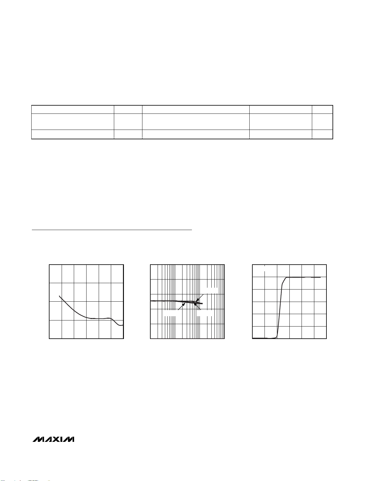
Typical Operating Characteristics
(VIN= 3V, CIN= 4.7µF, CX= 0.47µF, C
OUT
= 4.7µF, C
EXT
= 4.7µF, RCS= 0.4Ω, TA= +25°C, unless otherwise noted.)
NO-LOAD SUPPLY CURRENT
vs. SUPPLY VOLTAGE
MAX5008 toc01
SUPPLY VOLTAGE (V)
SUPPLY CURRENT (mA)
5.04.54.03.53.0
0.5
1.0
1.5
2.0
0
2.5 5.5
OUTPUT VOLTAGE
vs. LOAD CURRENT
MAX5008 toc02
LOAD CURRENT (mA)
OUTPUT VOLTAGE (V)
10010
4.7
4.9
5.1
5.3
5.5
4.5
11000
VIN = 2.9V
VIN = 5.0V
VIN = 3.3V
OUTPUT VOLTAGE
vs. SUPPLY VOLTAGE
MAX5008 toc03
SUPPLY VOLTAGE (V)
OUTPUT VOLTAGE (V)
54321
1
2
3
4
5
6
0
06
I
LOAD
= 100mA
PARAMETER SYMBOL CONDITIONS MIN TYP MAX UNITS
Thermal Shutdown
Junction Temperature
Thermal Shutdown Hysteresis 30 °C
150 °C
Page 4

MAX5008
Regulated 5V USB Charge Pump with
Programmable Current Limit
4 _______________________________________________________________________________________
Typical Operating Characteristics (continued)
(VIN= 3V, CIN= 4.7µF, CX= 0.47µF, C
OUT
= 4.7µF, C
EXT
= 4.7µF, RCS= 0.4Ω, TA= +25°C, unless otherwise noted.)
EFFICIENCY
vs. LOAD CURRENT
100
VIN = 2.95V
90
80
70
60
50
40
EFFICIENCY (%)
30
20
10
0
1 1000
VIN = 3.3V
LOAD CURRENT (mA)
10010
MAX5008 toc04
OUTPUT WAVEFORM
200ns/div
MAX5008 toc05
10mV/div
5V
0
5V
0
SHUTDOWN TIMING
1ms/div
MAX5008 toc06
RL = 46Ω
V
OUT
SHDN
LINE-TRANSIENT RESPONSE
I
= 100mA
LOAD
3.6V
3.1V
40µs/div
A: INPUT VOLTAGE: 500mV/div
B: OUTPUT VOLTAGE: AC-COUPLED, 100mV/div
MAX5008 toc07
LOAD-TRANSIENT RESPONSE
100mA
10mA
A
B
40µs/div
A: LOAD CURRENT
B: OUTPUT VOLTAGE: AC-COUPLED, 100mV/div
MAX5008 toc08
A
B
Page 5
Detailed Description
The MAX5008 charge pump provides a regulated 5V
output from a 2.95V to 5.5V input. The device delivers a
maximum of 125mA load current. Designed specifically
for compact applications, a complete regulator circuit
requires a minimum number of external components.
Adjustable Current Limit
The MAX5008 has an adjustable overcurrent protection. An external current-sense resistor is connected
from RCS to OUT to set the current limit. The current
limit is defined by:
I
LIMIT
= VCS/ RCS
where V
CS
is the current-sense trip level, typically 60mV.
For example, I
LIMIT
= 150mA when RCS = 0.40Ω.
When the output current limit is exceeded, the output
voltage falls and the device maintains the average output current at I
LIMIT
. Upon removal of the overcurrent
condition, the part resumes normal operation.
FAULT
Indication
When I
OUT
> I
LIMIT
or V
OUT
< VTH, FAULT asserts.
FAULT is an open-drain output that needs to be connected through a 100kΩ (typ) pullup resistor to a logic
supply voltage.
Thermal Shutdown
The MAX5008 has internal thermal shutdown circuitry,
which shuts down the device when the die temperature
exceeds +150°C. The thermal shutdown circuitry has
30°C hysteresis.
Shutdown Mode
Driving SHDN low places the device in shutdown
mode, which disables the oscillator, the control logic,
and the reference. The output goes into high-impedance state and drops to ground if loaded. Placing the
device in shutdown mode reduces the supply current
to less than 0.1µA. In normal operation, SHDN is driven
high or connected to IN.
Applications Information
Capacitor Selection
The MAX5008 requires four external capacitors. Their
values depend on the required output current. Table 1
shows the capacitor values recommended for different
load currents.
Input Voltage Range
The MAX5008 maintains a regulated 5V output with
input voltages from 2.95V to 5.5V. If the input voltage
exceeds 4.25V, limit the output current to 75mA or less.
This keeps the MAX5008 within its maximum power dissipation limits.
Layout Considerations
All capacitors should be located as close to the IC as
practical. Connect GND and PGND through a short,
MAX5008
Regulated 5V USB Charge Pump with
Programmable Current Limit
_______________________________________________________________________________________ 5
Table 1. Recommended Capacitor Values
Pin Description
PIN NAME FUNCTION
1 RCS
2 OUT Fixed 5V Output. Bypass OUT to GND with a 4.7µF capacitor.
3 FAULT
4 GND Ground Pin. Connect GND to PGND.
5 SHDN
6 PGND Power Ground Pin. Connect PGND to GND.
7 CXN Negative Terminal of the Charge-Pump Capacitor. Connect a 0.68µF capacitor from CXN to CXP.
8 IN Input Supply, 2.95V to 5.5V. Bypass IN to GND with a 4.7µF ceramic capacitor.
9 CXP Positive Terminal of the Charge-Pump Capacitor. Connect a 0.68µF capacitor from CXP to CXN.
10 CEXT Charge-Pump Output. Bypass CEXT to PGND with a 6.8µF capacitor.
External Current-Sense Resistor. Connect a resistor from RCS to OUT to set the overcurrent
threshold.
Output Fault Indicator. FAULT is asserted when either I
open-drain output that is high during normal operation or during shutdown.
Shutdown Input. When SHDN = low, the device turns off. Drive SHDN high or connect to IN for
normal operation.
I
LIMIT
= 60mV / RCS.
OUT
> I
LIMIT
or V
< VTH. FAULT is an
OUT
I
OUT
50mA 3.3 0.33 3.3 3.3
125 mA 4.7 0.68 6.8 4.7
C
(µF) CX (µF) C
IN
EXT
(µF) C
OUT
(µF)
Page 6
MAX5008
low-impedance trace, and connect the ground for CIN,
C
EXT
, and C
OUT
directly to PGND in a star configura-
tion. Connect RCSto C
EXT
through a short and low
impedance trace.
Chip Information
TRANSISTOR COUNT: 2632
PROCESS: BiCMOS
Regulated 5V USB Charge Pump with
Programmable Current Limit
6 _______________________________________________________________________________________
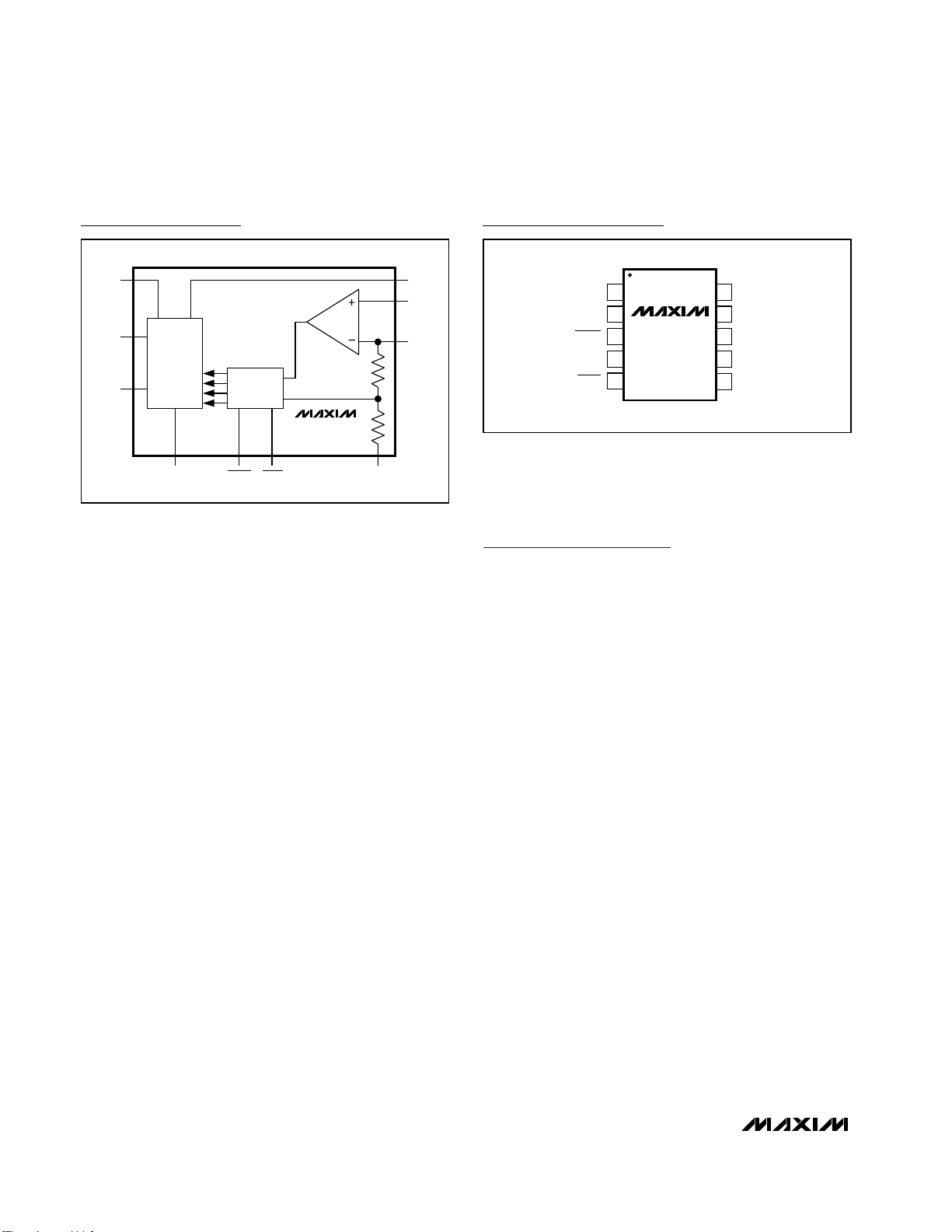
Pin Configuration
Functional Diagram
IN
CXN
SWITCHES
CXP
PGND FAULT
CONTROL
MAX5008
SHDN GND
CEXT
RCS
OUT
TOP VIEW
1
RCS
2
OUT
FAULT
MAX5008
3
4
5
µ
10
CEXT
9
CXP
8
IN
7
CXNGND
PGNDSHDN
6
MAX
Page 7
MAX5008
Regulated 5V USB Charge Pump with
Programmable Current Limit
Maxim cannot assume responsibility for use of any circuitry other than circuitry entirely embodied in a Maxim product. No circuit patent licenses are
implied. Maxim reserves the right to change the circuitry and specifications without notice at any time.
Maxim Integrated Products, 120 San Gabriel Drive, Sunnyvale, CA 94086 408-737-7600 _____________________ 7
© 2002 Maxim Integrated Products Printed USA is a registered trademark of Maxim Integrated Products.
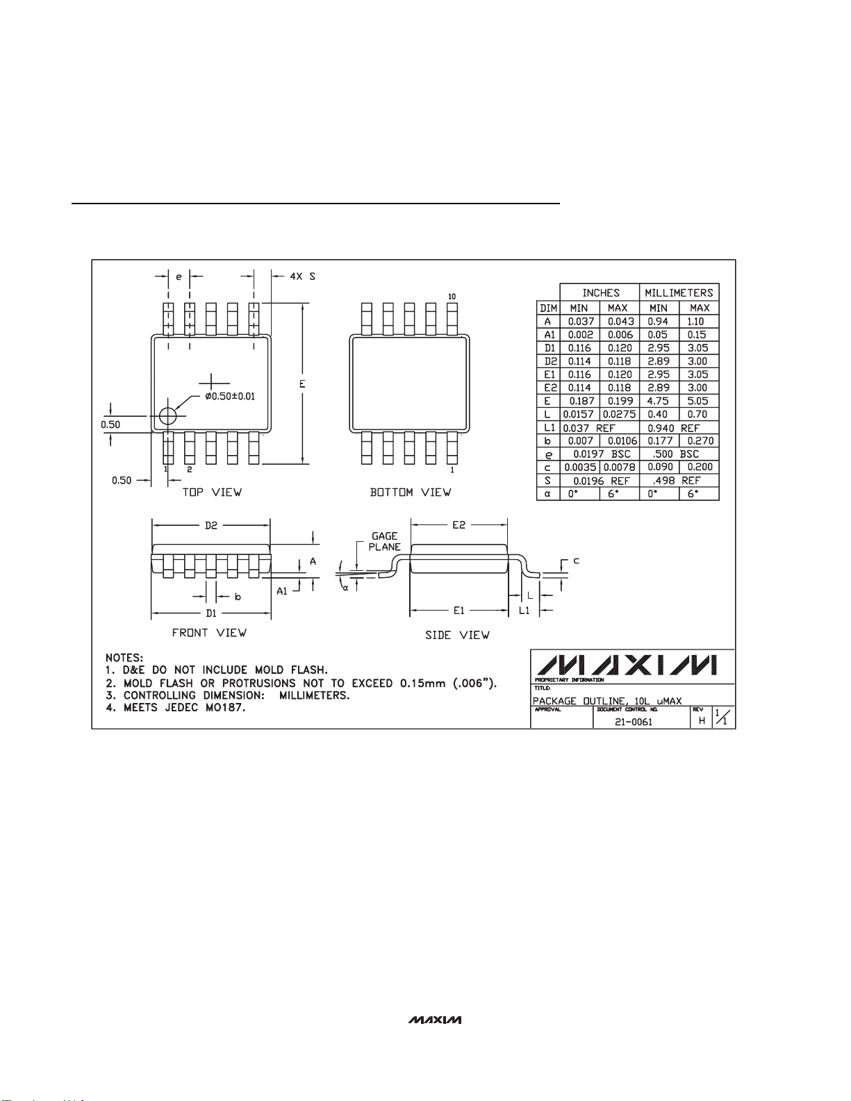
Package Information
(The package drawing(s) in this data sheet may not reflect the most current specifications. For the latest package outline information,
go to www.maxim-ic.com/packages.)
10LUMAX.EPS
 Loading...