

Page 1
现货库存、技术资料、百科信息、热点资讯,精彩尽在鼎好!
General Description
The MAX5005/MAX5006/MAX5007 are low-dropout
(LDO), micropower linear voltage regulators with an
integrated microprocessor (µP) reset circuit for use with
USB peripheral devices. Each device is available with a
fixed +3.3V output voltage and can deliver up to
150mA load current. Each device features ±15kV transient voltage suppression (TVS) as well as precision
1.5kΩ data-line termination resistors for USB digital signals making them ideal for use with USB peripherals.
The MAX5005/MAX5006/MAX5007 include an internal
reset circuit that enables the USB microcontroller
100ms after the LDO regulator output voltage reaches
regulation. Reset outputs are available in push-pull
(active-low or active-high) and open-drain (active-low)
options.
The MAX5005/MAX5006/MAX5007 are optimized for
use with a 1µF ceramic output capacitor. Each device
includes thermal shutdown protection, output short-circuit protection, and output to input reverse leakage protection. These devices also include an active-low
manual reset input.
The MAX5005 features an open-drain reset output, the
MAX5006 features an active-low push-pull reset output,
and the MAX5007 features an active-high push-pull
reset output. Each device is available in a space-saving
10-pin µMAX package.
Applications
USB Peripherals
Hand-Held Instruments
Features
♦ Integrated ±15kV Transient Voltage Suppressors
for D+ and D- Data Lines
♦ Pin Selectable Internal D+ and D- Termination
Resistors (1.5kΩ ±5%)
♦ Integrated Microprocessor Reset Circuit with
100ms (min) Timeout
♦ 3.3V Output with ±3% Accuracy
♦ 25µA Quiescent Current at Full Load
♦ Small 1µF Output Capacitor
♦ Output to Input Reverse Leakage Protection
♦ Thermal and Short-Circuit Protection
♦ 10-Pin µMAX Package
MAX5005/MAX5006/MAX5007
150mA USB LDO Regulators with ±15kV TVS
and µP Reset
________________________________________________________________ Maxim Integrated Products 1
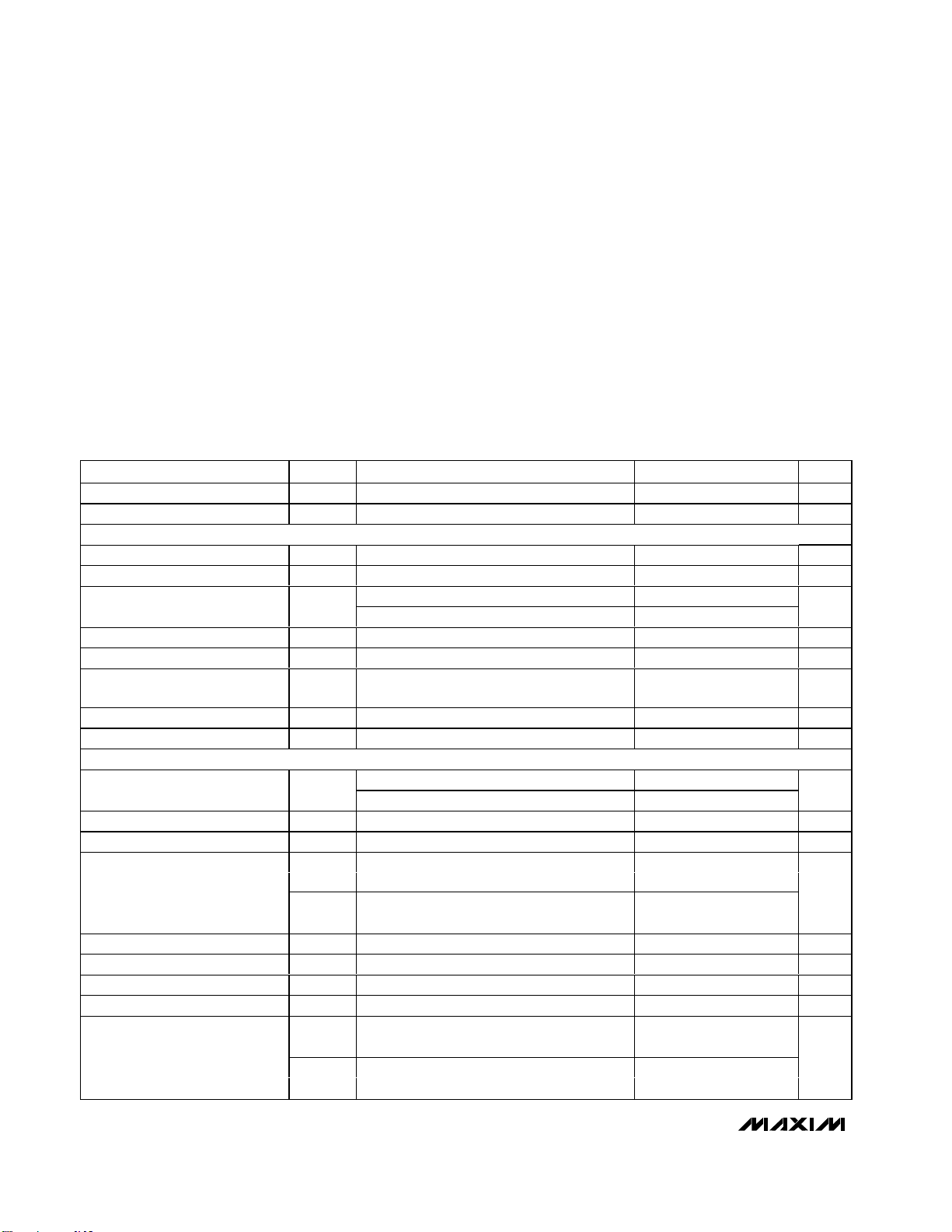
Pin Configuration
Ordering Information
19-2035; Rev 1; 11/02
*Insert “A” for a 7.5% reset threshold and “B” for a 12.5% reset
threshold.
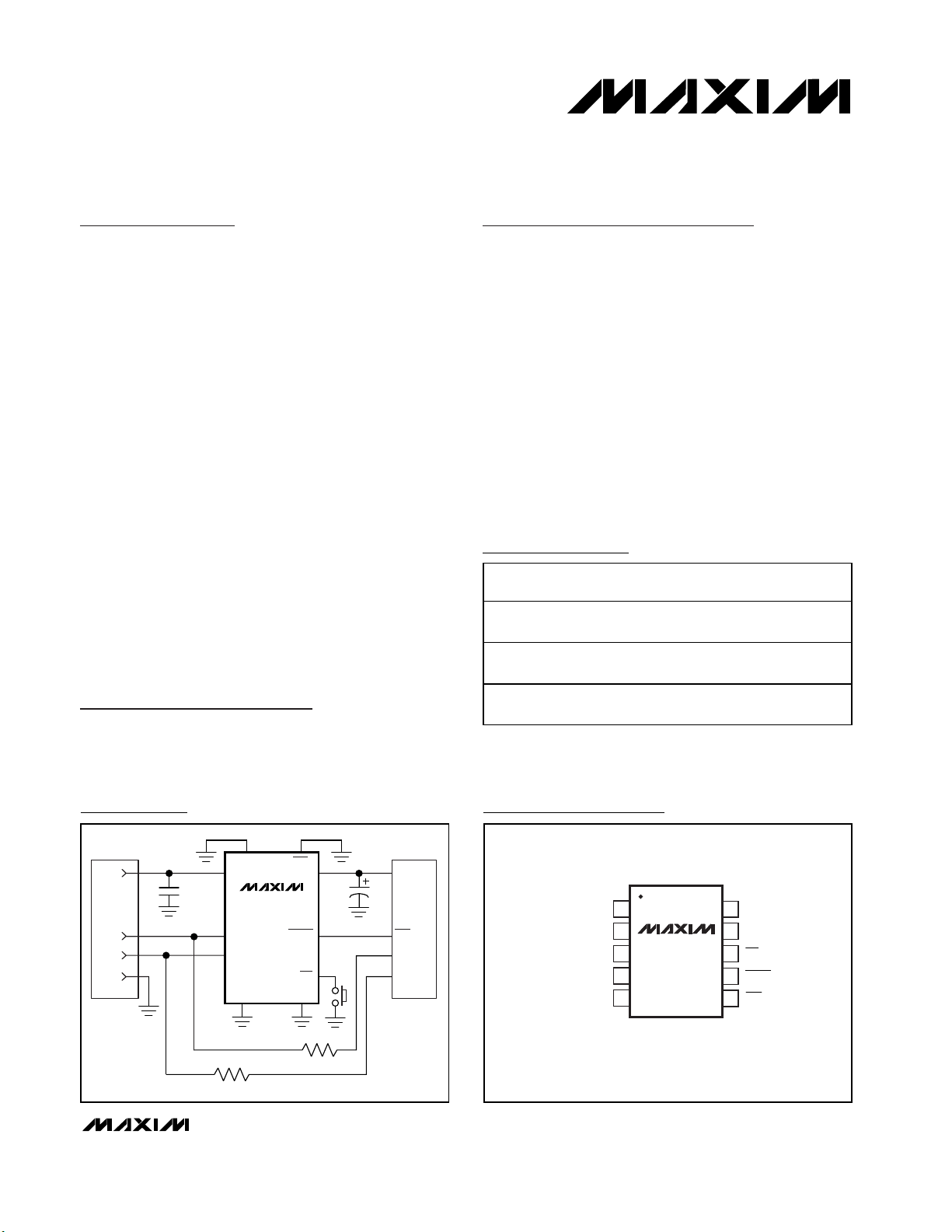
Typical Operating Circuit
For pricing, delivery, and ordering information, please contact Maxim/Dallas Direct! at
1-888-629-4642, or visit Maxim’s website at www.maxim-ic.com.
PART
MAX5005_CUB* 0°C to +70°C 10 µMAX
MAX5006_CUB* 0°C to +70°C 10 µMAX
MAX5007_CUB* 0°C to +70°C 10 µMAX
TEMP
RANGE
PINPACKAGE
RESET
OUTPUT
Op en-
D r ai n Low
Push-Pull
Low
Push-Pull
High
USB
PORT
V
BUS
C
IN
D+
D-
GND
( ) FOR MAX5007 ONLY
SELR
5V
1µF
CERAMIC
IN
D-
GND GND
27Ω
MAX5005
MAX5006
MAX5007
ENR
OUT
RESET
(RESET)
MR
27Ω
3.3V
C
OUT
1µF
3.3V USB
CONTROLLER
V
CC
RSTD+
D+
D-
TOP VIEW
1
IN
2
D+
3
GND
4
5
() FOR MAX5007 ONLY.
10
OUT
9
MAX5005
MAX5006
MAX5007
µMAX
GND
8
MR
7
RESET/(RESET)D-
ENRSELR
6
Page 2
MAX5005/MAX5006/MAX5007
150mA USB LDO Regulators with ±15kV TVS
and µP Reset
2 _______________________________________________________________________________________
ABSOLUTE MAXIMUM RATINGS
ELECTRICAL CHARACTERISTICS
(VIN= +5V, I
OUT
= 0, C
OUT
= 2.2µF, TA= 0°C to +70°C, unless otherwise noted. Typical specifications are at TA= +25°C.) (Note 1)
Stresses beyond those listed under “Absolute Maximum Ratings” may cause permanent damage to the device. These are stress ratings only, and functional
operation of the device at these or any other conditions beyond those indicated in the operational sections of the specifications is not implied. Exposure to
absolute maximum rating conditions for extended periods may affect device reliability.
IN to GND .................................................................-0.3V to +6V
D+, D- to GND..........................................................-0.3V to +6V
MR to GND ..............................................-0.3V to (V
OUT
+ 0.3V)
RESET, RESET to GND, Push-Pull............-0.3V to (V
OUT
+ 0.3V)
RESET to GND, Open-Drain.....................................-0.3V to +6V
OUT, SELR, ENR to GND .........................................-0.3V to +6V
Maximum Current to Any Pin
(except IN, OUT, D+, D-).............................................± 20mA
Short-Circuit Duration ....................................................Indefinite
Continuous Power Dissipation (T
A
= +70°C)
10-Pin µMAX (derate 5.6mW/°C above +70°C) ...........444mW
Thermal Resistance (θ
JA
)...............................................180°C/W
Operating Temperature Range...............................0°C to +70°C
Junction Temperature......................................................+150°C
Storage Temperature Range .............................-65°C to +150°C
Lead Temperature (soldering, 10s) .................................+300°C
Input Voltage Range V
Supply Current I
REGULATOR
Guaranteed Output Current I
Output Voltage V
Dropout Voltage (Note 2) ∆V
Output Current Limit VIN = 5.5V 165 350 mA
Input Reverse Leakage Current VIN = 0, V
Startup Response Time
Thermal Shutdown Temperature T
Thermal Shutdown Hysteresis ∆ T
RESET CIRCUIT
Reset Threshold (Note 3) V
Reset Timeout Period t
V
to Reset Delay t
OUT
MR Input Voltage
MR Minimum Input Pulse Width 1 µs
MR Glitch Rejection 120 ns
MR to Reset Delay 500 ns
MR Pullup Resistance to OUT 10 25 45 kΩ
SELR Input Voltage
PARAMETER SYMBOL CONDITIONS MIN TYP MAX UNITS
I
IN
GND
OUT
OUT
DO
= 100mA 4.0 5.5 V
LOAD
Measured at GND 25 50 µA
VIN = 4.0V to 5.5V, I
I
= 10mA 20 30
LOAD
I
= 150mA 300 400
LOAD
OUT
Rising edge of V
R
= 500Ω
L
JSHDN
JSHD N
MAX500_ACUB 2.92 3.05 3.18
TH
MAX500_BCUB 2.75 2.89 3.01
RP
RD
V
IL
V
IH
V
V
IL
IH
Connects R
Connects R
TERM
TERM
150 mA
= 0 to 100mA 3.2 3.3 3.4 V
OUT
= 5.5V 1 µA
to V
IN
OUT
500 µs
160
20
100 200 300 ms
75 µs
0.2 x
V
OUT
0.8 x
V
OUT
to D-
to D+
0.8 x
V
OUT
0.2 x
V
OUT
mV
o
o
V
V
V
C
C
Page 3
MAX5005/MAX5006/MAX5007
150mA USB LDO Regulators with ±15kV TVS
and µP Reset
_______________________________________________________________________________________ 3
ELECTRICAL CHARACTERISTICS (continued)
(VIN= +5V, I
OUT
= 0, C
OUT
= 2.2µF, TA= 0°C to +70°C, unless otherwise noted. Typical specifications are at TA= +25°C.) (Note 1)
Note 1: All devices are 100% tested at T
A
= +25°C. Limits over temperature are guaranteed by characterization and not production
tested.
Note 2: Dropout voltage is defined as V
IN
- V
OUT
when V
OUT
is 2% below the value of V
OUT
for VIN= V
OUT
+ 1V.
Note 3: Specification is guaranteed to ±4σ limit.
PARAMETER SYMBOL CONDITIONS MIN TYP MAX UNITS
SELR Input Current SELR = GND or OUT -1 1 µA
0.2 x
V
OUT
V
ENR Input Voltage
V
V
R
IL
IH
TERM
R
TERM
enabled
disabled
0.8 x
V
OUT
ENR Input Current ENR = GND or OUT -1 1 µA
Open-Drain RESET Output Low
Voltage (MAX5005)
Open-Drain Reset Output Leakage
Current (MAX5005)
Push-Pull RESET Output Voltage
(MAX5006)
Push-Pull RESET Output Voltage
(MAX5007)
V
I
LKG
V
V
V
V
> 1.0V, I
V
OUT
OUT
> 2.7V, I
OL
Reset not asserted -1.0 1.0 µA
V
= 1.0V, I
OUT
OL
V
> V
OUT
TH(MIN)
asserted
V
> V
OUT
OUT
OUT
TH(MAX)
> V
TH(MAX)
= 1.0V, I
OH
OL
OH
reset not asserted
V
reset not asserted
V
asserted
= 50µA, reset asserted 0.3
SINK
= 3.2mA, reset asserted 0.4
SINK
= 50µA, reset asserted 0.3
SINK
, I
= 3.2mA, reset
SINK
, I
SOURCE
, I
SINK
SOURCE
= 500µA,
= 3.2mA,
= 150µA, reset
0.8 x
V
OUT
0.8 x
V
OUT
0.4
0.4
V
V
V
V
USB OPTIONS AND TRANSIENT SUPPRESSION
D+/D- R
D+/D- Input Leakage Current V
D+ to D- Capacitance
D+, D- Capacitance to GND
Impedance ENR = GND, SELR = GND or OUT 1425 1500 1575 Ω
TERM
= V
ENR
1MHz, 100mVp-p signal
= 3.3V -1 1 µA
OUT
ENR = OUT 5.5
applied at D+ and D-,
= 3.3V
V
OUT
1MHz, 100mVp-p signal
Unpowered 24
ENR = OUT 40
applied at D+ and D-,
V
OUT
= 3.3V
Unpowered 47
pF
pF
ESD Trigger Voltage dV/dt < 1V/ns, VD+ or VD- > 3.6V 3.6 5 V
Surge Trigger Voltage dV/dt < 2V/µs, VD+ or VD- > 3.6V 3.6 16 V
Clamping Voltage 6A, pulse width = 200ns to 40µs16V
Surge Current 16V, pulse width = 200ns to 40µs ±6A
Human Body Model MIL-STD-883 ±16
D+/D- to GND ESD
Contact Discharge IEC1000-4-2
(EN61000-4-2)
±8
kV
Air Discharge IEC1000-4-2 (EN61000-4-2) ±15
Page 4
MAX5005/MAX5006/MAX5007
150mA USB LDO Regulators with ±15kV TVS
and µP Reset
4 _______________________________________________________________________________________
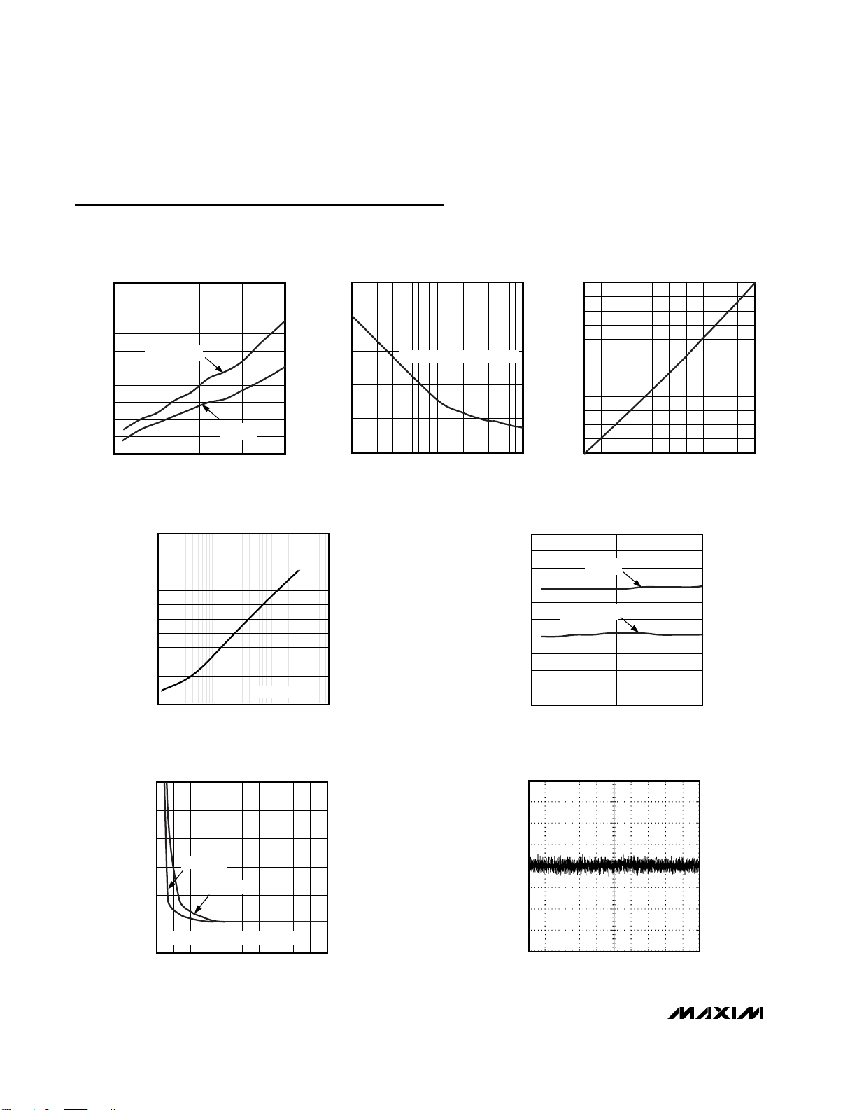
Typical Operating Characteristics
(VIN= +5V, I
OUT
= 0, C
OUT
= 2.2µF, unless otherwise noted.)
27.0
26.5
26.0
25.5
25.0
24.5
24.0
23.5
GROUND-PIN CURRENT (µA)
23.0
22.5
22.0
3.5 4.0 4.5 5.0 5.5
GROUND-PIN CURRENT
vs. SUPPLY VOLTAGE
I
= 150mA
OUT
SUPPLY VOLTAGE (V)
MAXIMUM PULSE DURATION vs.
RESET THRESHOLD OVERDRIVE
250
200
MAX5005-7 toc01
150
100
PULSE DURATION (µs)
I
= 0
OUT
50
0
110100
RESET THRESHOLD OVERDRIVE, VTH - V
RESET OCCURS ABOVE THIS LINE
(mV)
OUT
300
275
250
MAX5005-7 toc02
225
200
175
150
125
100
DROPOUT VOLTAGE (mV)
75
50
25
0
0306090120 150
DROPOUT VOLTAGE
vs. LOAD CURRENT
4515 75 105 135
LOAD CURRENT (mA)
MAX5005-7 toc03
POWER-SUPPLY REJECTION RATIO vs.
FREQUENCY
0
-5
-10
-15
-20
-25
-30
PSRR (dB)
-35
-40
-45
-50
-55
-60
0.01 0.1
C
OUT
FREQUENCY (kHz)
REGION OF STABLE C
= 1µF
110
OUT
MAX5005-07 toc04
ESR vs. LOAD CURRENT
150
ESR (Ω)
C
OUT
125
100
C
= 1µF
75
50
OUT
C
OUT
= 4.7µF
MAX5005-7 toc06
OUTPUT VOLTAGE
vs. SUPPLY VOLTAGE
3.35
3.34
I
3.33
3.32
3.31
3.30
3.29
OUTPUT VOLTAGE (V)
3.28
3.27
3.26
3.25
I
3.5 4.0 4.5 5.0 5.5
= 0
OUT
= 150mA
OUT
SUPPLY VOLTAGE (V)
OUTPUT NOISE
V
OUT
1mV/div
MAX5005-7 toc05
MAX5005-7 toc07
25
STABLE REGION BELOW THE CURVE
0
0604515 30 75 90 105 120 135 150
LOAD CURRENT (mA)
200µs/div
Page 5

MAX5005/MAX5006/MAX5007
150mA USB LDO Regulators with ±15kV TVS
and µP Reset
_______________________________________________________________________________________ 5
Typical Operating Characteristics (continued)
(VIN= +5V, I
OUT
= 0, C
OUT
= 2.2µF, unless otherwise noted.)
1.0ms/div
LOAD-TRANSIENT RESPONSE
3.3V
3.3V
MAX5005-7 toc10a
I
LOAD
V
OUT
50mV/div
V
OUT
50mV/div
C
OUT
= 2.2µF
C
OUT
= 1.0µF
20mA
0V
100µs/div
LINE-TRANSIENT RESPONSE
5.25V
4.75V
3.3V
MAX5005-7 toc11b
VIN
200mV/div
V
OUT
50mV/div
I
OUT
= 10mA
C
OUT
= 1µF
LOAD-TRANSIENT RESPONSE
MAX5005-7 toc10b
1.0ms/div
20mA
3.3V
3.3V
I
LOAD
V
OUT
50mV/div
C
OUT
= 10µF
C
OUT
= 4.7µF
V
OUT
50mV/div
0V
100
µs/div
LINE-TRANSIENT RESPONSE
4.75V
3.3V
MAX5005-7 toc11a
VIN
200mV/div
5.25V
V
OUT
50mV/div
I
OUT
= 10mA
C
OUT
= IµF
50ms/div
TURN-ON/TURN-OFF RESPONSE
MAX5005-7 toc08
VIN
5V/div
RESET
5V/div
RL = 1kΩ
V
OUT
5V/div
1ms/div
STARTUP RESPONSE
MAX5005-7 toc09
V
IN
5V/div
V
OUT
1V/div
RL = 1kΩ
TVS PEAK POWER vs. PULSE WIDTH
1000
100
PEAK POWER (W)
10
D+ OR D- WITH RESPECT TO GROUND
1
0.01 1 100
0.1 10
PULSE WIDTH (µs)
MAX5005-7 toc12
Page 6

MAX5005/MAX5006/MAX5007
150mA USB LDO Regulators with ±15kV TVS
and µP Reset
6 _______________________________________________________________________________________
Pin Description
PIN NAME DESCRIPTION
1IN
2D+
3, 9 GND
4D-
5 SELR
6 ENR
RESET
7
RESET
8 MR
10 OUT
Regulator Input. Supply voltage ranges from +4.0V to +5.5V. Bypass with a 1µF ceramic capacitor
to ground.
D+ ESD/Transient Suppression Input. Connect directly to USB port D+ data input. SELR high and
ENR low connects D+ to OUT through a 1.5kΩ resistor.
Ground. This pin also functions as a heatsink. Solder to large pads or the circuit board ground
plane to maximize thermal dissipation.
D- ESD/Transient Suppression Input. Connect directly to USB port D- data input. SELR low and
ENR low connects D- to OUT through a 1.5kΩ resistor.
USB Full-Speed/Low-Speed Termination Resistor Select. Logic high connects the termination
resistor to D+ for full-speed peripherals. Logic low connects the termination resistor to D- for lowspeed peripherals. An internal 1.5kΩ resistor connects to OUT when ENR is low.
USB Termination Resistor Enable. When reset is not asserted, ENR low enables the termination
resistor connection. ENR high or a reset disables the termination resistor connection.
Active-Low Reset Output. RESET remains low while V
is held low. RESET remains low for the duration of the reset timeout period after the reset conditions
are terminated. (MAX5005/MAX5006 ONLY)
Active-High Reset Output. RESET remains high while V
is held low. RESET remains high for the duration of the reset timeout period after the reset
conditions are terminated. (MAX5007 ONLY)
Active-Low Manual Reset Input. A logic low forces a reset. Reset remains asserted for the duration
of the reset timeout period after MR transitions from low to high. Leave unconnected or connect to
OUT if not used. MR has an internal pullup resistor of 25kΩ to OUT.
Voltage Regulator Output. Fixed +3.3V. Sources up to 150mA. Bypass with a 1µF (min) capacitor
for full rated performance.
is below the reset threshold or while MR
OUT
is below the reset threshold or while MR
OUT
Page 7

MAX5005/MAX5006/MAX5007
150mA USB LDO Regulators with ±15kV TVS
and µP Reset
_______________________________________________________________________________________ 7
Detailed Description
The MAX5005/MAX5006/MAX5007 are USB application-specific, low-dropout, low-quiescent current linear
regulators with an integrated µP reset circuit (see
Figure 1). The devices drive loads up to 150mA and
are available with a fixed output voltage of +3.3V.
Features include 1.5kΩ D+ and D- termination resistors
and ±15kV transient voltage suppression (TVS) in
accordance with IEC1000-4-2 (EN61000-4-2) Air
Discharge Method and MILSTD883C- Method 3015-6
making the MAX5005/MAX5006/MAX5007 ideal for use
with USB peripheral devices. The internal reset circuit
monitors the regulator output voltage and asserts a
reset signal when the output is typically -7.5% out of
regulation for MAX500_ACUB and -12.5% out of regulation for MAX500_BCUB.
Reset Circuit
The reset supervisor circuit is fully integrated in the
MAX5005/MAX5006/MAX5007, and uses the same reference voltage as the regulator. Two supply tolerance
reset thresholds, typically -7.5% and -12.5%, are available for each type of device.
7.5% reset: Reset does not assert until the regulator
output voltage is at least -3.6% out of tolerance and
always asserts before the regulator output voltage is
-11.5% out of tolerance.
12.5% reset: Reset does not assert until the regulator
output voltage is at least -8.8% out of tolerance and
always asserts before the regulator output voltage is
-16.7% out of tolerance.
Reset Output
The MAX5005/MAX5006/MAX5007 µP supervisory circuits assert a reset during power-up, power-down, and
Figure 1. Functional Diagram
THERMAL
LIMIT
ERROR
LDO
AMP
PROTECTION
ESD/
SURGE
PROTECTION
OUT
3.3V
4.0V to 5.5V
IN
REVERSE
CURRENT
PROTECTION
MAX5005
MAX5006
MAX5007
CURRENT
PROTECTION
V
REF
1.23V
GND
FULL
SPEED
D+
TVS
COMPARATOR
USB
TERMINATION
DRIVER
SELR
ENR
RESET
GND
200ms
RESET
TIMEOUT
LOW
SPEED
1.5kΩ1.5kΩ
( ) FOR MAX5007 ONLY.
OUTOUT
TVS
RESET/(RESET)
25kΩ
MR
D-
Page 8

MAX5005/MAX5006/MAX5007
150mA USB LDO Regulators with ±15kV TVS
and µP Reset
8 _______________________________________________________________________________________
brownout conditions. Reset is guaranteed to be logic
high or low depending on the device chosen (see
Ordering Information). RESET or RESET asserts when
V
OUT
is below the reset threshold and remains assert-
ed for at least 100ms minimum after V
OUT
rises above
the reset threshold. RESET or RESET also asserts when
MR is pulled low.
SELR and
ENR
When reset is not asserted a logic high to SELR connects a 1.5kΩ termination resistor from D+ to OUT for
full speed USB peripherals and a logic low connects a
1.5kΩ termination resistor from D- to OUT for low-speed
peripherals. Logic low on ENR enables the selected
termination resistor connection and logic high disables
the selected termination resistor connection. An asserted reset always disconnects the termination resistors.
D+ and D-
D+ and D- include transient voltage suppressors rated
at ±15kV (see USB ±15kV Transient Voltage
Suppression section).
The proprietary TVS shunt circuit passes no data
through the MAX5005/MAX5006/MAX5007, thereby
eliminating delays associated with series protection circuits. D+ and D- have only 1µA of leakage current and
a typical input capacitance of 40pF at 1MHz.
Manual Reset Input
Many µP-based products require manual reset capability, allowing the operator, a test technician, or external
logic circuitry to initiate a reset. A logic low on MR
asserts a reset while the regulator output voltage is still
within tolerance.
Reset remains asserted while MR is low and for the
reset timeout period (100ms minimum) after MR returns
high. The MR input has an internal pullup of 25kΩ (typ)
to OUT. Drive this input with TTL/CMOS logic levels or
with open-drain/collector outputs. Connect a normally
open momentary switch from MR to GND to create a
manual reset function; external debounce circuitry is
not required. If MR is driven from long cables or the
device is used in a noisy environment, connect a 0.1µF
capacitor from MR to GND to provide additional noise
immunity. For proper operation, ensure that the voltage
on MR is not greater than a diode drop above V
OUT
.
Output to Input Reverse Leakage
Protection
An internal circuit monitors the input and output voltages. When the output voltage is greater than the input
voltage, the internal pass transistor and parasitic
diodes turn off, and OUT powers the device. There is
no leakage path from OUT to IN. Therefore, the output
can be powered from an auxiliary supply such as a
backup battery without any need for additional blocking
diodes.
Current Limit
The MAX5005/MAX5006/MAX5007 include a current
limiter that monitors and controls the pass transistor’s
gate voltage, limiting the output current to 350mA (typ).
For design purposes, consider the current limit to be
160mA (min) to 600mA (max). The output can be shorted to ground for an indefinite period without damaging
the part.
Thermal Protection
When the junction temperature exceeds TJ= +160°C,
an internal thermal sensor signals the shutdown logic,
turning off the pass transistor and allowing the IC to
cool. The thermal sensor turns the pass transistor on
again after the IC’s junction temperature decreases by
20°C, resulting in a pulsed output during continuous
thermal overload conditions. Thermal overload protection is designed to protect the MAX5005/MAX5006/
MAX5007 in the event of fault conditions. For continuous operation, do not exceed the absolute maximum
junction temperature rating of T
J
= +150°C.
Operating Region and Power Dissipation
The MAX5005/MAX5006/MAX5007’s maximum power
dissipation depends on the thermal resistance of the
case and circuit board, the temperature difference
between the die junction and the ambient air, and the
rate of airflow. The power dissipation across the device
is P = I
OUT(VIN
- V
OUT
). The maximum power dissipa-
tion is:
P
MAX
= (TJ- TA) / (ΘJA)
where TJ- TAis the temperature difference between
the die junction and the surrounding air, Θ
JA
is the ther-
mal resistance of the package from junction to ambient.
The MAX5005/MAX5006/MAX5007’s ground pin (GND)
performs the dual function of providing an electrical
connection to the system ground and channeling heat
away. Connect GND to the system ground using a
large pad or ground plane. For optimum performance,
minimize trace inductance to D+, D-, and GND.
Applications Information
Capacitor Selection and Regulator
Stability
For stable operation over the full temperature range
and with load currents up to 150mA, use a 1µF (min)
output capacitor. To reduce noise and improve load
transient response, stability, and power-supply rejection, use large output capacitor values such as 10µF.
Page 9

MAX5005/MAX5006/MAX5007
150mA USB LDO Regulators with ±15kV TVS
and µP Reset
_______________________________________________________________________________________ 9
Note that some ceramic dielectrics exhibit large capacitance and ESR variation with temperature. With
dielectrics such as Z5U and Y5V, it may be necessary
to use 2.2µF or more to ensure stability at temperatures
below -10°C. With X7R or X5R dielectrics, 1µF should
be sufficient at all operating temperatures. Also, for
high-ESR tantalum capacitors, 2.2µF or more may be
needed to maintain stability. A graph of the Region of
Stable C
OUT
ESR vs. Load Current is shown in the
Typical Operating Characteristics.
To improve power-supply rejection and transient
response use a 1µF capacitor between IN and GND.
Negative-Going V
OUT
Transients
These devices are relatively immune to short-duration,
negative-going V
OUT
transients. The Typical Operating
Characteristics section shows a graph of the Maximum
Pulse Duration vs. Reset Threshold Overdrive for which
reset is not asserted. The graph was produced using
negative going output transients starting at V
OUT
and
ending below the reset threshold by the magnitude
indicated (Reset Threshold Overdrive). The graph
shows the maximum pulse width that a negative going
V
OUT
transient can typically have without triggering a
reset pulse. As the amplitude of the transient increases
(i.e., goes further below the reset threshold), the maximum allowable pulse width decreases. Typically, a
V
OUT
transient that goes only 10mV below the reset
threshold and lasts for 75µs will not trigger a reset
pulse.
USB ±15kV Transient Voltage
Suppression
The universal serial bus (USB) simplifies interconnectivity between peripheral devices and personal computers. USBs offer high-speed data communication rates
(up to 12Mbps) using only two lines (D+ and D-).
CMOS based USB peripherals that utilize deep submicron technologies are more susceptible to electrostatic
discharge (ESD) failure due to shorter channel lengths,
shallower drain/source junctions, and lightly doped
drain structures. The MAX5005/MAX5006/MAX5007
incorporate a proprietary transient voltage suppression
(TVS) circuit for use with submicron devices.
The TVS design complies with IEC-1000-4-2 level 4
(EN61000-4-2) ±15kV Air Discharge and ±8kV Contact
Discharge as well as MIL STD 883C-Method 3015-6
level 3.
The TVS circuit handles up to 11A of surge current. The
TVS/ESD structure is directly coupled to the output of
the LDO regulator.
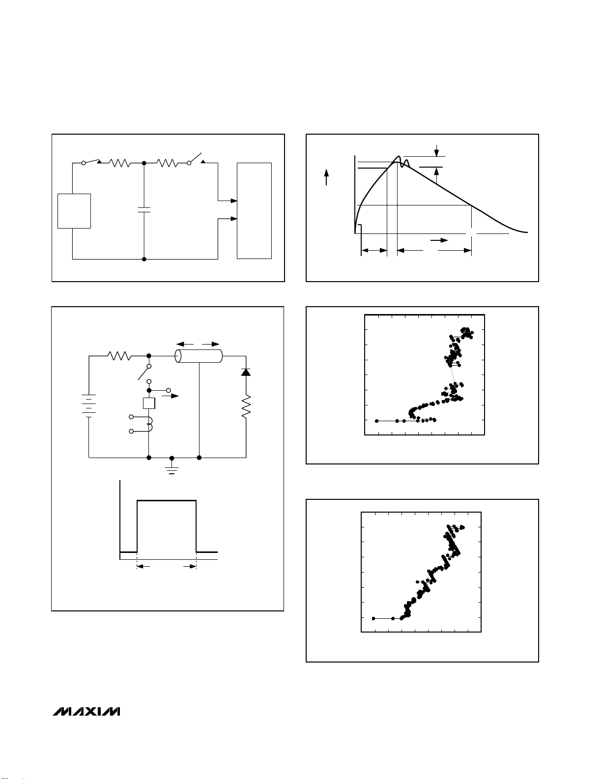
TVS Surge Test Information
Figure 2 shows the test circuit used to generate the
8/40µs short circuit waveform of Figure 3. Figures 4, 5,
and 6 show the actual surge current I/V characteristics
with various capacitive loads.
ESD Performance
The MAX5005/MAX5006/MAX5007 are characterized
to the following limits on D+, D-, and IN:
• ±15kV using the Human Body Model
• ±8kV using the Contact Discharge Method specified
in IEC 1000-4-2 (EN61000-4-2)
•±15kV using the Air-Gap Discharge Method specified in IEC 1000-4-2 (EN61000-4-2).
Note that in order to achieve the above ESD levels on
IN, a ceramic 1µF ceramic capacitor should be connected from IN to GND.
ESD Test Conditions
ESD performance depends on several conditions.
Contact Maxim for a reliability report that documents
test setup, methodology, and results.
Human Body Model
Figure 7 shows the Human Body Model, and Figure 8
shows the current waveform it generates when discharged into low impedance. This model consists of a
100pF capacitor charged to the ESD voltage of interest,
which is then discharged into the test device through a
1.5kΩ resistor.
ESD Transmission Line Pulsing
Figure 9 shows the test circuit used for transmission
line pulsing conditions. The 200ns pulsewidth has a
rise time of 4ns. Figure 10 shows the Current vs.
Voltage characteristics for various output capacitance
values.
Page 10

MAX5005/MAX5006/MAX5007
150mA USB LDO Regulators with ±15kV TVS
and µP Reset
10 ______________________________________________________________________________________
Figure 2. Surge Current Test Circut
Figure 4. Surge Current I/V Characteristic (C
OUT
= 0)
Figure 5. Surge Current I/V Characteristic (C
OUT
= 1µF)
Figure 6. Surge Current I/V Characteristic (C
OUT
= 10µF)
Figure 3. Test Circuit Surge Current Waveform (Short-Circuit
Load)
JENNINGS
200kΩ 20Ω
HIGH
VOLTAGE
RELAY
RF3D-26S
2µF
4kV
80µH
12
10
8
6
4
CURRENT (A)
2
0
= 0
C
OUT
D+ OR D- TO GND
8/40µs PULSE WIDTH
D+/D-
TVS
DEVICE
UNDER
TEST
0.2µF
LEAKAGE
RELAY
IP 100%
AMPERES
50%
0
0
8µs
t
1
40µs
t
TIME
2
12
10
8/40µs PULSE WIDTH
8
6
4
D+ OR D- TO GND
CURRENT (A)
2
0
C
= 1µF
OUT
12
10
8
6
4
CURRENT (A)
2
0
24608101614 1812 20
VOLTAGE (V)
8/40µs PULSE WIDTH
= 10µF
C
OUT
D+ OR D- TO GND
24608101614 1812
VOLTAGE (V)
24608101614 1812
VOLTAGE (V)
Page 11
MAX5005/MAX5006/MAX5007
150mA USB LDO Regulators with ±15kV TVS
and µP Reset
______________________________________________________________________________________ 11
Figure 9. Transmission Line Pulsing Setup for ESD I/V
Characteristics
Figure 11. Transmission Line Pulsing I/V Characteristic
(C
OUT
= 1µF)
Figure 10. Transmission Line Pulsing I/V Characteristic
(C
OUT
= 0)
Figure 7. Human Body ESD Test Model
Figure 8. Human Body Model Current Waveform
R
D
1500Ω
DISCHARGE
RESISTANCE
STORAGE
CAPACITOR
HIGH-
VOLTAGE
DC
SOURCE
R
C
1MΩ
CHARGE-CURRENT
LIMIT RESISTOR
C
100pF
s
10MΩ
SCOPE
V
IN
DEVICE
L
Zo = 50Ω
DEVICE
UNDER
TEST
R
IP 100%
90%
AMPERES
36.8%
10%
0
0
t
RL
TIME
t
DL
CURRENT WAVEFORM
7
6
D+ OR D- TO GND
= 0
C
5
4
3
CURRENT (A)
2
L
1
0
OUT
200ns PULSE WIDTH
PEAK-TO-PEAK RINGING
I
r
(NOT DRAWN TO SCALE)
= 4ns
t
RISE
t
= 200ns
pw
4602 810121416
VOLTAGE (V)
7
6
D+ OR D- TO GND
= 1µF
C
OUT
5
200ns PULSE WIDTH
4
3
CURRENT (A)
2
1
0
4602 810121416
VOLTAGE (V)
Page 12

MAX5005/MAX5006/MAX5007
150mA USB LDO Regulators with ±15kV TVS
and µP Reset
12 ______________________________________________________________________________________
Chip Information
TRANSISTOR COUNT: 890
PROCESS: BiCMOS
Figure 12. Transmission Line Pulsing I/V Characteristic
(C
OUT
= 10µF)
7
6
D+ OR D- TO GND
C
= 10µF
OUT
5
200ns PULSE WIDTH
4
3
CURRENT (A)
2
1
0
4602 810121416
VOLTAGE (V)
Page 13

MAX5005/MAX5006/MAX5007
150mA USB LDO Regulators with ±15kV TVS
and µP Reset
Maxim cannot assume responsibility for use of any circuitry other than circuitry entirely embodied in a Maxim product. No circuit patent licenses are
implied. Maxim reserves the right to change the circuitry and specifications without notice at any time.
Maxim Integrated Products, 120 San Gabriel Drive, Sunnyvale, CA 94086 408-737-7600 ____________________ 13
© 2002 Maxim Integrated Products Printed USA is a registered trademark of Maxim Integrated Products.
Package Information
(The package drawing(s) in this data sheet may not reflect the most current specifications. For the latest package outline information
go to www.maxim-ic.com/packages.)
0.6±0.1
e
10
ÿ0.50 ±0.1
1
0.6±0.1
TOP VIEW
D2
A2
b
D1
FRONT VIEW
4X S
10
DIM
H
1
e
BOTTOM VIEW
α
E2
GAGE PLANE
A
A1
α
E1
L
L1
INCHES
MIN
-A
0.002
A1
A2 0.030 0.037 0.75 0.95
0.116
D1
0.114
D2
0.116
E1
0.114
E2
0.187
H
0.0157
L
L1
0.037 REF
0.007
b
0.0197 BSC
0.0035
c
0.0196 REF
S
0∞ 0∞ 6∞
c
MAX
0.043
0.006
0.120
0.118
0.120
0.118
0.199
0.0275
0.0106
0.0078
6∞
MILLIMETERS
MAX
MIN
-
1.10
0.05
0.15
2.95
3.05
2.89
3.00
2.95
3.05
2.89
3.00
4.75
5.05
0.40
0.70
0.940 REF
0.177
0.270
0.500 BSC
0.090
0.200
0.498 REF
SIDE VIEW
10LUMAX.EPS
PROPRIETARY INFORMATION
TITLE:
PACKAGE OUTLINE, 10L uMAX/uSOP
REV.DOCUMENT CONTROL NO.APPROVAL
21-0061
1
I
1
 Loading...