

For free samples & the latest literature: http://www.maxim-ic.com, or phone 1-800-998-8800.
For small orders, phone 1-800-835-8769.
General Description
The MAX5003 high-voltage switching power-supply
controller has all the features and building blocks needed for a cost-effective flyback and forward voltagemode control converter. This device can be used to
design both isolated and nonisolated power supplies
with multiple output voltages that operate from a wide
range of voltage sources. It includes a high-voltage
internal start-up circuit that operates from a wide 11V to
110V input range. The MAX5003 drives an external Nchannel power MOSFET and has a current-sense pin
that detects overcurrent conditions and turns off the
power switch when the current-limit threshold is
exceeded. The choice of external power MOSFET and
other external components determines output voltage
and power.
The MAX5003 offers some distinctive advantages: softstart, undervoltage lockout, external frequency synchronization, and fast input voltage feed-forward. The
device is designed to operate at up to 300kHz switching frequency. This allows use of miniature magnetic
components and low-profile capacitors. Undervoltage
lockout, soft-start, switching frequency, maximum duty
cycle, and overcurrent protection limit are all adjustable
using a minimum number of external components. In
systems with multiple controllers, the MAX5003 can be
externally synchronized to operate from a common system clock.
Warning: The MAX5003 is designed to operate with
high voltages. Exercise caution.
The MAX5003 is available in 16-pin SO and QSOP packages. An evaluation kit (MAX5003EVKIT) is also available.
Applications
Telecommunication Power Supplies
ISDN Power Supplies
+42V Automobile Systems
High-Voltage Power-Supply Modules
Industrial Power Supplies
Features
♦ Wide Input Range: 11V to 110V
♦ Internal High-Voltage Startup Circuit
♦ Externally Adjustable Settings
Output Switch Current Limit
Oscillator Frequency
Soft-Start
Undervoltage Lockout
Maximum Duty Cycle
♦ Low External Component Count
♦ External Frequency Synchronization
♦ Primary or Secondary Regulation
♦ Input Feed-Forward for Fast Line-Transient
Response
♦ Precision ±2.5% Reference over Rated
Temperature Range
MAX5003
High-Voltage PWM
Power-Supply Controller
________________________________________________________________ Maxim Integrated Products 1
19-1555; Rev 0; 12/99
PART
MAX5003CEE
MAX5003CSE
MAX5003EEE -40°C to +85°C
0°C to +70°C
0°C to +70°C
TEMP. RANGE PIN-PACKAGE
16 QSOP
16 Narrow SO
16 QSOP
EVALUATION KIT
AVAILABLE
Note A: Dice are designed to operate over a -40°C to +140°C
junction temperature (T
j
) range, but are tested and guaranteed at
TA= +25°C.
Pin Configuration
Ordering Information
MAX5003ESE -40°C to +85°C 16 Narrow SO
MAX5003C/D (Note A) Dice
TOP VIEW
1
V+ V
INDIV
2
ES
3
4
FREQ
SS
5
REF
6
CON
7
COMP
8
QSOP/Narrow SO
16
DD
V
15
CC
NDRV
14
MAX5003
13
12
11
10
9
PGND
CS
AGND
MAXTON
FB
MAX5003
High-Voltage PWM
Power-Supply Controller
2 _______________________________________________________________________________________
ABSOLUTE MAXIMUM RATINGS
ELECTRICAL CHARACTERISTICS
(V+ = VES= VDD= +12V, V
INDIV
= 2V, V
CON
= 0, R
FREQ
= R
MAXTON
= 200kΩ, TA= T
MIN
to T
MAX
, unless otherwise noted. Typical
values are at T
A
= +25°C.)
Stresses beyond those listed under “Absolute Maximum Ratings” may cause permanent damage to the device. These are stress ratings only, and functional
operation of the device at these or any other conditions beyond those indicated in the operational sections of the specifications is not implied. Exposure to
absolute maximum rating conditions for extended periods may affect device reliability.
V+ to GND ............................................................-0.3V to +120V
ES to GND ..............................................................-0.3V to +40V
VDDto GND............................................................-0.3V to +19V
VCCto GND.........................................................-0.3V to +12.5V
MAXTON, COMP, CS, FB, CON to GND..................-0.3V to +8V
NDRV, SS, FREQ to GND...........................-0.3V to (V
CC
+ 0.3V)
I
NDIV
, REF to GND.................................................-0.3V to +4.5V
VCC, VDD, V+, ES Current ................................................±20mA
NDRV Current, Continuous...............................................±25mA
NDRV Current, ≤ 1µs .............................................................±1A
CON and REF Current ......................................................±20mA
All Other Pins ....................................................................±20mA
Continuous Power Dissipation (T
A
= +70°C)
16-Pin SO (derate 9.5mW/°C above +70°C)...............762mW
16-Pin QSOP (derate 8.3mW/°C above +70°C)..........667mW
Maximum Junction Temperature (TJ) ..............................+150°C
Operating Temperature Ranges
MAX5003C_E ....................................................0°C to +70°C
MAX5003E_E ..................................................-40°C to +85°C
Operating Junction Temperature (T
J
) .............................+125°C
16-Pin SO θJA.................................................................105°C/W
16-Pin QSOP θ
JA
............................................................120°C/W
Storage Temperature Range .............................-65°C to +150°C
Lead Temperature (soldering, 10s) .................................+300°C
I
REF
= 0 to 1mA
No load
V+ = VES, VDD= 18.75
I
NDRV
= 50 mA
V
INDIV
= 0, V+ = 110V, VES= VDD=
unconnected
I
NDRV
= 50 mA
V
NDRV
= V
CC
V
NDRV
= 0, VCCsupported by VCCcapacitor
V+ = 36V, ES = unconnected,
VDD= 18.75V
VCCfalling
V+ = 36V, IV+< 75µA,
ES = unconnected
V+ = VES= 36V, I
NDRV
= 7.5mA
V+ = 110V, VDD= unconnected
V+ = 36V, IDD= 0 to 7.5mA,
ES = unconnected
mV
520
∆V
REF
REF Voltage Regulation
V
2.905 3.000 3.098
V
REF
REF Output Voltage
Ω
1
R
OL
NDRV Resistance Low
Ω
412
R
OH
NDRV Resistance High
mA
1000
Peak Sink Current
mA
570
Peak Source Current
V
6.3
V
CCLO
VCCUndervoltage
Lockout Voltage
V
CC
VCCOutput Voltage
mA
1.2
I
DD
µA
35 75
I+Shutdown Current
Supply Current
V
7.4 12
V
10.75
V
TO
VDDRegulator Turn-Off Voltage
V
10.75 18.75
V
DD
VDDInput Voltage Range
V
25
V
10.8 36
V
ESI
ESInput Voltage (Note 1)
V
36
V
ESO
ESOutput Voltage
V
9 9.75 10.5
V
DD
VDDOutput Voltage
CONDITIONS UNITSMIN TYP MAXSYMBOL PARAMETER
VDD= unconnected, V+ = VES, I
NDRV
= 7.5mA
V110
V+V+ Input Voltage (Note 1)
ES= VDD= unconnected
REFERENCE
OUTPUT DRIVER
CHIP SUPPLY (VCC)
PREREGULATOR/START-UP
SUPPLY CURRENT
I
NDRV
= 2mA
I
NDRV
= 5mA
MAX5003
High-Voltage PWM
Power-Supply Controller
_______________________________________________________________________________________ 3
ELECTRICAL CHARACTERISTICS (continued)
(V+ = VES= VDD= +12V, V
INDIV
= 2V, V
CON
= 0, R
FREQ
= R
MAXTON
= 200kΩ, TA= T
MIN to TMAX
, unless otherwise noted. Typical
values are at T
A
= +25°C.)
(Note 2)
V
FREQ
= 5V, V
CON
= 3.0V
V
CON
= 3.0V
V
CON
= 3.0V
From end of blanking time 25mV overdrive
0 < VCS< 0.1V
V
INDIV
= 1.28V
FB = COMP, V
CON
= 1.5V
V+ = VES= VDD=
10.8V and 18.75V
At COMP
At COMP
I
COMP
= 5µA; V
COMP
= 0.5V, 2.5V
R
LOAD
= 200kΩ, C
LOAD
= 100pF
A
VOL
= 1V/V, C
LOAD
= 100pF
VFB= 1.5V
kHz
200 1200
f
FREQ
FREQ Range
µs
813
t
EXT
External Oscillator Maximum
Low Time
µA
1
I
OL
FREQ Output Low
V
2.7
V
IH
FREQ Input High
V
0.8
V
IL
FREQ Input Low
µA
-1 0.01 +1
INDIV Bias Current
mV
125
V
HYST
INDIV Hysteresis
1.23 1.32 1.45
V
1.15 1.20 1.25
V
INDIVLO
INDIV Undervoltage Lockout
ppm/°C
100
TC
FB
FB V
SET
Tempco
µA
-1 0.1 +1
I
FB
FB Bias Current
ns
70
t
B
CS Blanking Time
ns
240
t
D
µA
-1 +1
I
CS
CS Input Bias Current
Overcurrent Delay
V
1.448 1.485 1.522
V
SET
FB Regulation Voltage
V
3.00
V
COMPH
Output Clamp High
V
0.25
V
COMPL
Output Clamp Low
dB
60 80
A
V
Voltage Gain
MHz
1.2
BWUnity-Gain Bandwidth
degrees
65
φ
Phase Margin
fS = 1/4 f
FREQ
ns
150
FREQ HI/LO Pulse Width
kHz
50 300
f
S
Frequency Range
CONDITIONS UNITS MIN TYP MAXSYMBOLPARAMETERS
V
FREQ
= 1.5V
V
FREQ
= 0
µA
1
I
OL
FREQ Output Current Low
µA
300
I
OH
FREQ Output Current High
kHz
80 100 120
Oscillator Frequency
kΩ
50 500
R
FREQ
FREQ Resistor Range
V
INDIV
= 1.25V %
75
Maximum Programmable
Duty Cycle
V
CON
= 1.25V mV
80 100 120
V
CS
CS Threshold Voltage
MAXIMUM DUTY CYCLE (MAXTON)
MAIN OSCILLATOR—INTERNAL MODE
MAIN OSCILLATOR—EXTERNAL MODE
UNDERVOLTAGE LOCKOUT
FEEDBACK INPUT AND SET POINT
ERROR AMPLIFIER
CURRENT LIMIT
V
INDIV
falling
V
INDIV
rising
0.8
-0.4
-0.6
0
-0.2
0.6
0.4
0.2
0.8
0-20 20 40 60 80 100
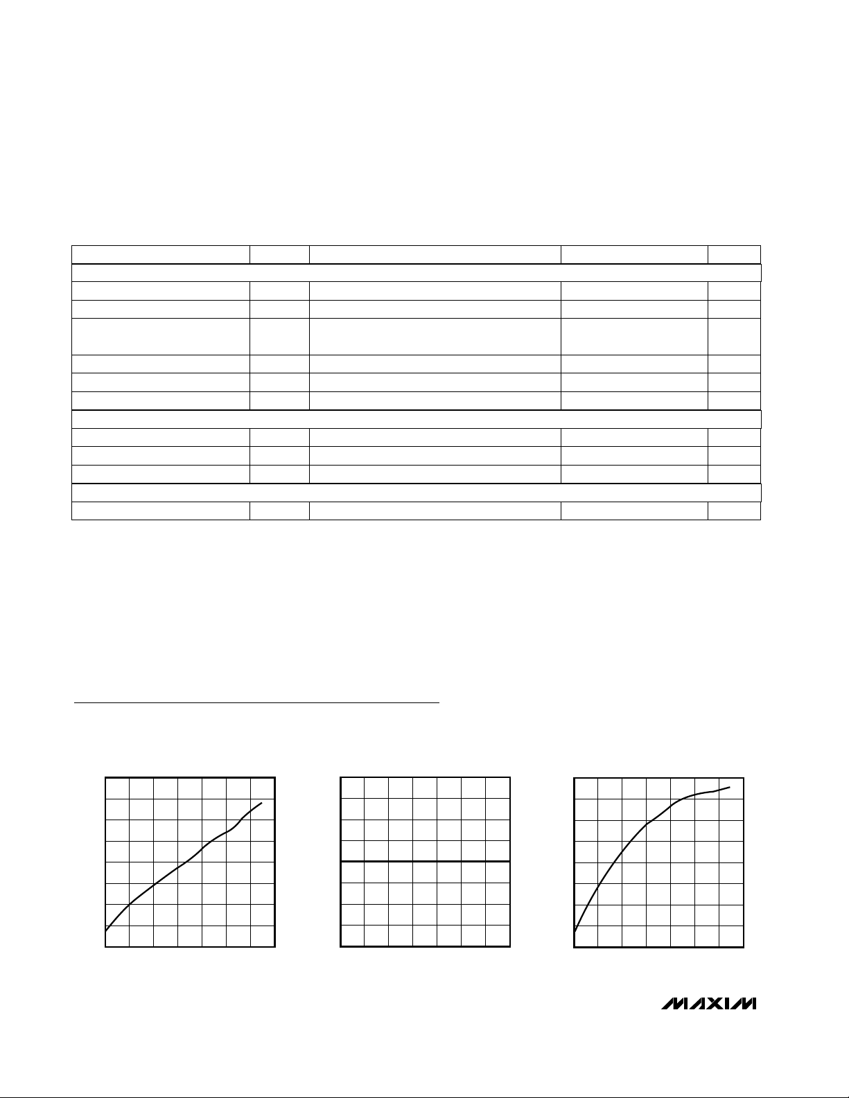
FB SET-POINT VOLTAGE CHANGE
vs. TEMPERATURE
MAX5003-01
TEMPERATURE (°C)
FB SET-POINT VOLTAGE CHANGE (%)
-0.100
-0.050
-0.075
0
-0.025
0.075
0.050
0.025
0.100
11 1312 14 15 16 17 18
FB SET-POINT VOLTAGE CHANGE
vs. SUPPLY VOLTAGE
MAX5003-02
VDD (V)
FB SET-POINT VOLTAGE CHANGE (%)
-1.20
-0.80
-1.00
-0.40
-0.60
0.20
0
-0.20
0.40
-40 0-20 20 40 60 80 100
SWITCHING FREQUENCY CHANGE
vs. TEMPERATURE
MAX5003-03
TEMPERATURE (°C)
FREQUENCY CHANGE (%)
Typical Operating Characteristics
(VDD= +12V, R
FREQ
= 200kΩ, R
MAXTON
= 200kΩ, TA= +25°C, unless otherwise noted.)
MAX5003
High-Voltage PWM
Power-Supply Controller
4 _______________________________________________________________________________________
ELECTRICAL CHARACTERISTICS (continued)
(V+ = V
ES
=
VDD= +12V, V
INDIV
= 2V, V
CON
= 0, R
FREQ
= R
MAXTON
= 200kΩ, TA= T
MIN
to T
MAX
, unless otherwise noted. Typical
values are at T
A
= +25°C.)
Note 1: See the Typical Operating Characteristics for preregulator current-to-voltage characteristics.
Note 2: Maximum time FREQ can be held below V
IL
and still remain in external mode.
Note 3: Feed-forward Ratio = Duty cycle at (V
INDIV
= 1.5V)/Duty cycle at (V
INDIV
= 1.875V)
Note 4: Occurs at start-up and until V
REF
is valid.
CONDITIONS UNITS MIN TYP MAXSYMBOLPARAMETERS
Minimum On-Time
200
ns
SS Source Current VSS= 0.5V, VDD= unconnected, V
CON
= 1.5V
3.4 5.5 9
µA
SS Sink Current V
SS
= 0.4V (Note 4)
10
mA
SS Time
0.45
s/µF
CON Bias Current I
CON
V
CON
= 0.5V and 2.5V
-1 0.01 1
µA
R
MAXTON
= 200kΩ, V
INDIV
= 1.25V µs
7.5
t
ON
Maximum On-Time Range
V
INDIV
= 1.875V V
0.48 0.5 0.53
RAMP Voltage Low
V
2.5
RAMP Voltage High
V
INDIV
stepped from 1.5V to 1.875V, V
CON
=
3.0V (Note 3)
0.72 0.8 0.88
Input Voltage Feed Forward
Ratio
kΩ50 500R
MAXTON
MAXTON Resistor Range
PWM COMPARATOR
SOFT-START
PWM OSCILLATOR
MAX5003
High-Voltage PWM
Power-Supply Controller
_______________________________________________________________________________________ 5
Typical Operating Characteristics (continued)
(VDD= +12V, R
FREQ
= 200kΩ, R
MAXTON
= 200kΩ, TA= +25°C, unless otherwise noted.)
V+ INPUT CURRENT vs. VOLTAGE
3.0
2.5
2.0
1.5
+ (mA)
V
I
1.0
0.5
V
= V
COMP
SWITCHING
= V
FB
V+ (V)
CON
0
20 6040 80 100 120
ERROR AMP FREQUENCY RESPONSE
70
60
50
40
30
20
GAIN (dB)
10
0
-10
-20
0.1k 1k 10k 100k 1M 10M
GAIN
FREQUENCY (Hz)
MAX5003-07
PHASE
MAX5003-04
0
-20
-40
-60
-80
-100
-120
-140
-160
-180
2.50
2.00
1.50
+ (mA)
V
I
1.00
0.50
0
400
350
300
250
200
150
PHASE (degrees)
FREQUENCY (kHz)
100
50
0
V+ INPUT CURRENT vs. TEMPERATURE
V
= V
CON
SWITCHING
V+ = 110V
-40 0-20 20 40 60 80 100
= V
COMP
FB
TEMPERATURE (°C)
SWITCHING FREQUENCY AND PERIOD
vs. R
FREQ
FREQUENCY
PERIOD
0 100 200 300
(kΩ)
R
FREQ
400
MAX5003-08
500
MAX5003-05
40
30
20
PERIOD (µs)
10
0
MAXIMUM DUTY CYCLE vs. V
80
70
60
50
40
30
DUTY CYCLE (%)
20
V
CLAMPED HIGH
CON
100kΩ
V
INDIV
10
0
123
V+ SHUTDOWN CURRENT
vs. TEMPERATURE
40
V+ = 110V
39
38
37
36
35
+ (µA)
V
I
34
33
32
31
30
= 0
V
INDIV
= UNCONNECTED
V
DD
-40 0-20 20 40 60 80 100
TEMPERATURE (°C)
400kΩ
(V)
INDIV
300kΩ
200kΩ
PARAMETER IS
R
MAXTON
4
MAX5003-06
5
MAX5003-09
V+ CURRENT IN BOOTSTRAPPED
OPERATION vs. TEMPERATURE
28.0
V+ = 110V
= 1.5V
V
INDIV
27.5
27.0
+ (µA)
V
I
26.5
26.0
-50 0 50 100
TEMPERATURE (°C)
MAX5003-10
(V)
V
10
9
8
7
6
5
CC
4
3
2
1
0
VCC LOAD REGULATION
V+ = 50V TO 110V
V+ = 12V
V+ = 13V
V+ = 14V
V+ = 15V
ES = UNCONNECTED
= UNCONNECTED
V
DD
0 5 10 15 20
ICC (mA)
MAX5003-11

MAX5003
High-Voltage PWM
Power-Supply Controller
6 _______________________________________________________________________________________
Pin Description
Typical Operating Characteristics (continued)
(VDD= +12V, R
FREQ
= 200kΩ, R
MAXTON
= 200kΩ, TA= +25°C, unless otherwise noted.)
NAME FUNCTION
1 V+
Preregulator Input. Connect to the power line for use with 25V to 110V line voltages. Bypass V+ to ground
with a 0.1µF capacitor, close to the IC. Connects internally to the drain of a depletion FET preregulator.
2 INDIV
Undervoltage Sensing and Feed-Forward Input. Connect to the center point of an external resistive divider
connected between the main power line and AGND. Undervoltage lockout takes over and shuts down
the controller when V
INDIV
< 1.2V. INDIV bias is typically 0.01µA.
PIN
3 ES
Preregulator Output. When V+ ranges above 36V, bypass ES to AGND with a 0.1µF capacitor close to
the IC. When V+ is always below 36V, connect ES to V+.
4 FREQ
Oscillator Frequency Adjust and Synchronization Input. In internal free-running mode, the voltage on this
pin is internally regulated to 1.25V. Connect a resistor between this pin and AGND to set the PWM frequency. Drive between V
IL
and VIHat four times the desired frequency for external synchronization.
8 COMP Compensation Connection. Output of the error amplifier, available for compensation.
7 CON Control Input of the PWM Comparator
6 REF Reference Voltage Output (3.0V). Bypass to AGND with a 0.1µF capacitor.
5 SS
Soft-Start Capacitor Connection. Ramp time to full current limit is approximately 0.5ms/nF. Limits duty
cycle when VSS< V
CON
.
10 MAXTON
Maximum On-Time Programming. A resistor from MAXTON to AGND sets the PWM gain and limits the
maximum duty cycle. The voltage on MAXTON tracks the voltage on the INDIV pin. Maximum on-time is
proportional to the value of the programming resistor. The maximum duty cycle is limited to 75%, regardless of the programming resistor.
9 FB Feedback Input. Regulates to VFB= V
REF
/ 2 = 1.5V.
(V)
CC
V
VCC LOAD REGULATION
10
9
8
7
6
5
4
3
2
V+ = V
=
ES
12V TO 36V
V
DD = UNCONNECTED
1
0
0 5 10 15 20
ICC (mA)
MAX5003-12
MAXIMUM FREQUENCY vs. INPUT VOLTAGE
AND FET TOTAL GATE-SWITCHING CHARGE
350
300
250
200
150
100
MAX SWITCHING FREQUENCY (kHz)
15nC
50
0
12 13 14
20nC
10nC
V+ (V)
30nC
25nC
15
MAX5003-13
16

MAX5003
High-Voltage PWM
Power-Supply Controller
_______________________________________________________________________________________ 7
Pin Description (continued)
NAME FUNCTIONPIN
13 PGND Power Ground. Connect to AGND.
12 CS
Current Sense with Blanking. Turns power switch off if VCSrises above 100mV (referenced to PGND).
Connect a 100Ω resistor between CS and the current-sense resistor (Figure 2). Connect CS to PGND if
not used.
11 AGND Analog Ground. Connect to PGND close to the IC.
14 NDRV Gate Drive for External N-Channel Power FET
15 V
CC
Output Driver Power-Rail Decoupling Point. Connect a capacitor to PGND with half the value used for
VDDbypass very close to the pin. If synchronizing several controllers, power the fan-out buffer driving the
FREQ pins from this pin.
16 V
DD
9.75V Internal Linear-Regulator Output. Drive VDDto a voltage higher than 10.75V to bootstrap the chip
supply. V
DD
is also the supply voltage rail for the chip. Bypass to AGND with a 5µF to 10µF capacitor.
Detailed Description
The MAX5003 is a PWM controller designed for use as
the control and regulation core of voltage-mode control
flyback converters or forward-voltage power converters. It provides the power-supply designer with maximum flexibility and ease of use. The device is specified
up to 110V and will operate from as low as 11V. Its
maximum operating frequency of 300kHz permits the
use of miniature magnetic components to minimize
board space. The range, polarity, and range of output
voltages and power are limited only by design and by
the external components used.
This device works in isolated and nonisolated configurations, and in applications with single or multiple output voltages. All the building blocks of a PWM
voltage-mode controller are present in the MAX5003
and its settings are adjustable. The functional diagram
is shown on Figure 1.
Modern Voltage-Mode Controllers
The MAX5003 offers a voltage-mode control topology
and adds features such as fast input voltage feed forward, programmable maximum duty cycle, and high
operating frequencies. It has all the advantages of current-mode control—good control loop bandwidth,
same-cycle response to input voltage changes, and
pulse-by-pulse current limiting. It eliminates disadvantages such as the need for ramp compensation, noise
sensitivity, and the analytical and design difficulties of
dealing with two nested feedback loops. In summary,
voltage-mode control has inherent superior noise
immunity and uses simpler compensation schemes.
Internal Power Regulators
The MAX5003’s power stages operate over a wide
range of supply voltages while maintaining low power
consumption. For the high end of the range (+36V to
+110V), power is fed to the V+ pin into a depletion
junction FET preregulator. This input must be decoupled with a 0.1µF capacitor to the power ground pin
(PGND). To decouple the power line, other large-value
capacitors must be placed next to the power transformer connection.
The preregulator drops the input voltage to a level low
enough to feed a first low-dropout regulator (LDO)
(Figure 1). The input to the LDO is brought out at the ES
pin. ES must also be decoupled with a 0.1µF capacitor.
In applications where the maximum input voltage is
below 36V, connect ES and V+ together and decouple
with a 0.1µF capacitor.
The first LDO generates the power for the VDDline. The
VDDline is available at the VDDpin for decoupling. The
bypass to AGND must be a 5µF to 10µF capacitor.
When the maximum input voltage is always below
18.75V, power may also be supplied at VDD; in this
case, connect V+, ES, and VDDtogether.
Forcing voltages at VDDabove 10.75V (see Electrical
Characteristics) disables the first LDO, typically reducing current consumption below 50µA (see Typical
Operating Characteristics).
Following the VDDLDO is another regulator that drives
VCC: the power bus for the internal logic, analog circuitry, and external power MOSFET driver. This regulator is needed because the VDDvoltage level would be
too high for the external N-channel MOSFET gate. The

MAX5003
High-Voltage PWM
Power-Supply Controller
8 _______________________________________________________________________________________
Figure 1. Functional Diagram
V
FETBIAS
1
V+
2
INDIV
ES
3
1.2V
AGND
UV LOCKOUT
HIGH-VOLTAGE EPIFET
V
V
CC
DD
V
OK
IN
MAX5003
V
ES
V
OK
IN
V
CC
REF
REFOK
SDN
LINEAR
REGULATOR
LINEAR
REGULATOR
OK
BANDGAP
REFERENCE
AGND
V
DD
AGND
V
CC
AGND
16
V
V
DD
V
CC
DD
V
15
CC
14
NDRV
FREQ
REF
CON
COMP
“1”
V
CC
4
5
SS
6
7
8
FREQ
REFOK
SDN
INDIV
MAXTON
RAMP
SS
V
CON
PWM COMP
SDN
CLK
RAMP
AGND
V
AGND
CC
V
REF
D “D”FF
CLK Q
R
C
LIMIT
V
CC
R
R
DRIVER
CURRENT
SENSE
CS BLANK
100ns
STRETCHING
V
CC
PGND
V
CC
PGND
V
CC
PGND
NDRV
0.1V
13
PGND
12
CS
11
AGND
10
MAXTON
9
FB
ERROR AMP
AGND

VCCregulator has a lockout line that shorts the N-channel MOSFET driver output to ground if the VCCLDO is
not regulating. VCCfeeds all circuits except the V
CC
lockout logic, the undervoltage lockout, and the power
regulators.
The preferred method for powering the MAX5003 is to
start with the high-voltage power source (at V+ or ES,
depending on the application), then use a bootstrap
source from the same converter with an output voltage
higher than the VDDregulator turn-off voltage (10.75V)
to power VDD. This will disable the power consumption
of the VDDLDO. It is also possible to power the
MAX5003 with no bootstrap source from ES or V+, but
do not exceed the maximum allowable power dissipation. The current consumption of the part is mostly a
function of the operating frequency and the type of
external power switch used—in particular, the total
charge to be supplied to the gate.
A reference output of 3V nominal is externally available
at the REF pin, with a current sourcing capability of
1mA. A lockout circuit shuts off the oscillator and the
output driver if REF falls 200mV below its set value.
Minimize loading at REF, since the REF voltage is the
source for the FB voltage, which is the regulator set
point when the error amplifier is used. Any changes in
V
REF
will be proportionally reflected in the regulated
output voltage of the converter.
Undervoltage Lockout, Feed Forward,
and Shutdown
The undervoltage lockout feature disables the controller
when the voltage at INDIV is below 1.2V (120mV hysteresis). When INDIV rises higher than 1.2V plus the
hysteresis (typically 1.32V), it allows the controller to
start. An external resistive divider connected between
the power line and AGND generates the INDIV signal.
INDIV is also used as the signal for the fast input voltage feed-forward circuit.
Always connect INDIV to a voltage divider. It is not a
“don’t care” condition; the signal is used to set the fast
feed-forward circuit (see the Oscillator and Ramp
Generator section).
Choose R2 (Figure 2) between 25kΩ to 500kΩ and calculate R1 to satisfy the following equation:
where V
SUL
= system undervoltage lockout and
V
INDIVLO
= I
NDIV
undervoltage lockout.
The undervoltage lockout function allows the use of the
INDIV pin as a shutdown pin with an external switch to
ground. The shutdown circuit must not affect the resistive divider during normal operation.
Current-Sense Comparator
The current-sense (CS) comparator and its associated
logic limit the current through the power switch. Current
is sensed at CS as a voltage across a sense resistor
between the external MOSFET source and PGND.
Connect CS to the external MOSFET source through a
100Ω resistor or RC lowpass filter (Figures 2 and 3).
See CS Resistor in the Component Selection section.
A blanking circuit shunts CS to ground when the power
MOSFET switch is turned off, and keeps it there for
70ns after turn-on. This avoids false trips caused by the
switching transients. The blanking circuit also resets
the RC filter, if used. When VCS> 100mV, the power
MOSFET is switched off. The propagation delay from
the time the switch current reaches the trip level to the
driver turn-off time is 240ns. If the current limit is not
used, the CS pin must be connected to PGND.
Error Amplifier
The internal error amplifier is one of the building blocks
that gives the MAX5003 its flexibility. Its noninverting
input is biased at 1.5V, derived from the internal 3V reference. The inverting input is brought outside (FB pin)
and is the regulation feedback connection point. If the
error amplifier is not used, connect this pin to ground.
The output is available for the frequency compensation
network and for connection to the input of the PWM
comparator (CON). Unity-gain frequency is 1.2MHz,
open-circuit gain is 80dB, and the amplifier is unitygain stable. To eliminate long overload recovery times,
there are clamps limiting the output excursions close to
the range limits of the PWM ramp. The voltage at the
noninverting input of the error amplifier is the regulator
set point, but is not accessible.
Set-point voltage can be measured, if needed, by connecting COMP and FB and measuring that node with
respect to ground. The error amplifier is powered from
the V
CC
rail.
PWM Comparator
The pulse-width modulator (PWM) comparator stage
transforms the error signal into a duty cycle by comparing
the error signal with a linear ramp. The ramp levels are
0.5V min and 2.5V max. The comparator has a typical
hysteresis of 5.6mV and a propagation delay of 100ns.
The output of the comparator controls the external FET.
Soft-Start
The soft-start feature allows converters built using the
MAX5003 to apply power to the load in a controllable
soft ramp, thus reducing start-up surges and stresses.
MAX5003
High-Voltage PWM
Power-Supply Controller
_______________________________________________________________________________________ 9
RR
12 1 =−
V
SUL
V
INDIVLO

MAX5003
It also determines power-up sequencing when several
converters are used.
Upon power turn-on, the SS pin acts as a current sink
to reset any capacitance attached to it. Once REF has
exceeded its lockout value, SS sources a current to the
external capacitor, allowing the converter output voltage to ramp up. Full output voltage is reached in
approximately 0.45s/µF.
The SS pin is an overriding extra input to the PWM
comparator. As long as its voltage is lower than V
CON
,
it overrides V
CON
and SS determines the level at which
the duty cycle is decided by the PWM comparator.
After exceeding V
CON
, SS no longer controls the duty
cycle. Its voltage will keep rising up to VCC.
Oscillator and Ramp Generator
The MAX5003 oscillator generates the ramp used by
the comparator, which in turn generates the PWM digital signal. It also controls the maximum on-time feature
of the controller. The oscillator can operate in two
modes: free running and synchronized (sync). A single
pin, FREQ, doubles as the attachment point for the frequency programming resistor and as the synchronization input. The mode recognition is automatic, based on
the voltage level at the FREQ pin.
In free-running mode, a 1.25V source is internally
applied to the pin; the oscillator frequency is proportional to the current out of the pin through the programming resistor, with a proportionality constant of
16kHz/µA.
In sync mode, the signal from the external master generator must be a digital rectangular waveform running
at four times the desired converter switching frequency.
Minimum acceptable signal pulse width is 150ns, positive or negative, and the maximum frequency is
1.2MHz.
When the voltage at FREQ is forced above 2.7V, the
oscillator goes into sync mode. If left at or below 1.5V for
more than 8µs to 20µs, it enters free-running mode.
The master clock generator cannot be allowed to stop
at logic zero. If the system design forces such a situation, an inverter must be used at the FREQ pin.
In sync mode, the oscillator signal is divided by four and
decoded. The output driver is blocked during the last
phase of the division cycle, giving a hardwired maximum
on-time of 75%. In free-running mode, the oscillator duty
cycle is 75% on, and the off portion also blocks the output driver. The maximum on-time is then absolutely limited to 75% in either mode. Maximum on-time can be
controlled to values lower than 75% by a programming
resistor at the MAXTON pin.
The PWM ramp generated goes from 0.5V min to 2.5V
max, and the maximum time on is the time it takes from
low to high.
MAXTON is internally driven to V
INDIV
and a resistor
must be connected from MAXTON to AGND, to program the maximum on-time.
The ramp slope is directly proportional to V
INDIV
and
inversely proportional to R
MAXTON
. Since the ramp voltage limits are fixed, controlling the ramp slope sets the
maximum time on.
Changing the ramp slope while V
CON
remains constant
also changes the duty cycle and the energy transferred to
the load per cycle of the converter. The INDIV signal is a
fraction of the input voltage, so the fast input voltage feedforward works by modifying the duty cycle in the same
clock period, in response to an input voltage change.
Calculate the maximum duty cycle as:
where:
D
MAX
= Maximum duty cycle (%)
MAXTON = Maximum on-time
T = Switching period
Then:
where:
R
MAXTON
= Resistor from the MAXTON pin to ground
V
INDIV
= Voltage at the INDIV pin
ƒSW= Output switching frequency
MAXTON can then be calculated as:
N-Channel MOSFET
Output Switch Driver
The MAX5003 output drives an N-channel MOSFET
transistor. The output sources and sinks relatively large
currents, supplying the gate with the charge the transistor needs to switch. These are current spikes only,
since after the switching transient is completed the load
is a high-value resistance. The current is supplied from
the VCCrail and must be sourced by a large-value
High-Voltage PWM
Power-Supply Controller
10 ______________________________________________________________________________________
D
MAX
D 0.75 100
= ⋅
MAX
MAXTON
=
MAXTON
= ⋅ 100
T
R
MAXTON
200k
075 125
. .
k V kHz
200 100
1.25V
Ω
V
RV
⋅⋅
MAXTON
Ω
⋅⋅
INDIV
INDIV
ƒ
SW
100kHz

capacitor (5µF to 10µF) at the VCCpin, since the rail will
not support such a load. It is this current, equivalent to
the product of the total gate switching charge (from the
N-channel MOSFET data sheet), times the operating
frequency, that determines the bulk of the MAX5003
power dissipation.
The driver can source up to 560mA and sink up to 1A
transient current with a typical on source resistance of
4Ω. The no-load output levels are VCCand PGND.
Applications Information
Compensation and Loop
Design Considerations
The circuit shown in Figure 2 is essentially an energy
pump. It stores energy in the magnetic core and the air
gap of the transformer while the power switch is on,
and delivers it to the load during the off phase. It can
operate in two modes: continuous and discontinuous.
In discontinuous mode, all the energy is given to the
load before the next cycle begins; in continuous mode,
some energy is continuously stored in the core.
The system has four operating parameters: input voltage, output voltage, load current, and duty cycle. The
PWM controller senses the output voltage and the input
voltage, and keeps the output voltage regulated by
controlling the duty cycle.
The output filter in this circuit consists of the load resistance and the capacitance on the output.
To study the stability of the feedback system and
design the compensation necessary for system stability
under all operating conditions, first determine the transfer function. In discontinuous mode, since there is no
energy stored in the inductor at the end of the cycle,
the inductor and capacitor do not show the characteristic double pole, and there is only a dominant pole
defined by the filter capacitor and the load resistance.
There is a zero at a higher frequency, defined by the
ESR of the output filter capacitor. Such a response is
easy to stabilize for a wide range of operating conditions while retaining a reasonably fast loop response.
In continuous mode, the situation is different. The
inductor-capacitor combination creates a double pole,
since energy is stored in the inductor at all times. In
addition to the double pole, a right-half-plane zero
appears in the frequency response curves. This
response is not easy to compensate. It can result in
conditional stability, a complicated compensation network, or very slow transient response.
To avoid the analytical and design problems of the continuous-conduction mode flyback topology and maintain
good loop response, choose a design incorporating a
discontinuous-conduction mode power stage
To keep the converter in discontinuous mode at all times,
the value of the power transformer’s primary inductance
must be calculated at minimum line voltage and maximum load, and the maximum duty cycle must be limited.
The MAX5003 has a programmable duty-cycle limit function intended for this purpose.
Design Methodology
Following is a general procedure for developing a system:
1) Determine the requirements.
2) In free-running mode, choose the FREQ pin programming resistor. In synchronized mode, determine
the clock frequency (f
CLK)
.
3) Determine the transformer turns ratio, and check the
maximum duty cycle.
4) Determine the transformer primary inductance.
5) Complete the transformer specifications by listing
the primary maximum current, the secondary maximum current, and the minimum duty cycle at full
power.
6) Choose the MAXTON pin programming resistor.
7) Choose a filter capacitor.
8) Determine the compensation network.
Design Example
1) 36V < VIN< 72V, V
OUT
= 5V, I
OUT
= 1A, ripple
< 50mV, settling time ≈ 0.5ms.
2) Generally, the higher the frequency, the smaller the
transformer. A higher frequency also gives higher
system bandwidth and faster settling time. The
trade-off is lower efficiency. In this example, 300kHz
switching frequency is the choice to favor for a small
transformer. If the converter will be free running (not
externally synchronized), use the following formula to
calculate the R
FREQ
programming resistor:
where:
R
FREQ
= Resistor between FREQ and ground
ƒSW= Switching frequency (300kHz)
If the converter is synchronized to an external clock,
the input frequency will be 1.2MHz. The external
clock runs at four times the desired switching frequency.
R
kHz
kk
FREQ
SW
=
ƒ
=
100
200 66 7 .Ω
MAX5003
High-Voltage PWM
Power-Supply Controller
______________________________________________________________________________________ 11

MAX5003
3) The main factors influencing the choice of the turns
ratio are the switch breakdown voltage and the duty
cycle. With a smaller turns ratio, the secondary
reflected voltage and the maximum voltage seen by
the switch during flyback are reduced, which is
favorable. On the other hand, a smaller turns ratio
will shorten the duty cycle and increase the primary
RMS current, which can impact efficiency. A good
starting figure is the ratio of the input voltage to the
output voltage, rounding to the nearest integer. To
keep the flyback voltage under control, choose an 8to-1 ratio for the 48V to 5V system. The maximum
duty cycle allowed without putting the device in continuous-conduction mode can be found using the following formula:
where:
N = NP/NS= Turns ratio
V
SEC
= Secondary voltage
DC
MAX
= Maximum duty cycle
V
MIN
= Minimum power-line voltage
For a 48V to 5V system with an 8-to-1 turns ratio, the
maximum duty cycle before putting the device in
discontinuous mode is 55%. Assume that VINmin is
36V (minimum input voltage, neglecting drops in the
power switch and in the resistance of the primary
coil) and V
SEC
is 5.4V (5V plus a Schottky diode
drop). The MAX5003 maximum duty cycle is internally limited to 75%. Generally this parameter must fall
between 45% to 65% to obtain a balance between
efficiency and flyback voltage while staying out of
continuous conduction. If the value exceeds these
bounds, adjust the turns ratio.
4) Assuming 80% efficiency, a 6.25W input is needed
to produce a 5W output. Set an operating duty cycle
around 12% below the maximum duty cycle to allow
for component variation: 55% - 12% = 43%. Use the
following formula to calculate the primary inductance:
L
DC V
PWR
V
W kHz
H
PRI
MIN
IN SW
=
()
ƒ
=
()
≅µ
⋅
⋅⋅⋅⋅⋅
22
2
04336
2 6 25 300
65
.
.
High-Voltage PWM
Power-Supply Controller
12 ______________________________________________________________________________________
Figure 2. Application Example 1: Nonisolated +48V to +5V Converter
+48V
(36V TO 72V)
V
IN
1M
1
0.1µF
39k
0.1µF
0V
62k
470nF
0.1µF
2
3
4
5
6
7
8
V+
INDIV
ES
FREQ
SS
REF
CON
COMP
390pF
C
MAX5003
F
V
V
NDRV
PGND
AGND
MAXTON
R
F
200k
DD
CC
CS
FB
XFACOILTRCTX03
2
L
P
65µH
0.1µF
R
CS
0.1Ω
5
IRFD620S
16
15
14
10µF
13
12
11
10
9
33µF
100Ω
51k
8
CMSD4448
7
11, 12
MBRS130L
9, 10
4.7µF
22µF
22µF
R
A
41.2k
R
B
17.4k
+5V
1A
DC
MAX
=
1
V
MIN
⋅
VN
SEC
1
+

where:
DC = Duty cycle. Set to calculated minimum duty
cycle at V
MIN.
PWRIN= Input power, at maximum output power
This gives an inductance value (L
PRI
) of approxi-
mately 65µH.
5) The other parameter that defines the transformer is
peak current. This is given by:
The peak secondary current is the peak primary current multiplied by the turns ratio, or 0.8A · 8 = 6.4A.
Calculating the minimum duty cycle:
With these numbers, the transformer manufacturer
can choose a core.
6) For this application, the MAX5003 must be programmed for a maximum duty cycle of 55% at 36V.
The MAX5003 will automatically scale the limit with
the reciprocal of the input voltage as it changes. The
duty-cycle limit for an input voltage of 72V will be
27% (half of 55%). The duty cycle needed to stay out
of continuous conduction at 72V is 37%, so there is a
10% margin. The maximum duty time scales with the
voltage at the undervoltage lockout pin, V
INDIV
. The
voltage at INDIV is set by selecting the power line
undervoltage lockout trip point. The trip point for this
system, running from 36V to 72V, is 32V. Then INDIV
must be connected to the center point of a divider
with a ratio of 32/1.25, connected between the
power line and ground. Then R
MAXTON
is:
MAX5003
High-Voltage PWM
Power-Supply Controller
______________________________________________________________________________________ 13
Figure 3. Application Example 2: Isolated -48V to +5V Converter
0V
0.1µF
39k
V
IN
-48V
-36V TO -72V
XFACOILTRCTX03
CMSD4448
2
L
P
65µH
33µF
100Ω
IRFD620S
0.1µF
R
CS
0.1Ω
R1
1M
1
V+
2
INDIV
3
ES
4
MAX5003
FREQ
5
SS
6
REF
7
CON
8
R2
0.1µF
62k
470nF
1.3k
0.1µF
COMP
V
V
NDRV
PGND
AGND
MAXTON
16
DD
15
CC
14
10µF
13
12
CS
11
10
9
FB
51k
8
4.7µF
7
5
MBRS130L
11, 12
9, 10
6
5
MDC217
22µF
7
240k
22µF
1
2
TL431
51Ω
680Ω
3900pF
0.01µF
24.9k
24.9k
+5V
1A
-
I
PRI
=
2 PWR
⋅
L
⋅
PRI SW
IN
ƒ
2 6.25W
==
⋅
65 H 300kHz
⋅
µ
0.8A
DC DC
% .%===⋅⋅43
MIN MAX
() ( )
V
IN MAX
()
V
IN MIN
()
36
72
V
21 5
V
V
R
MAXTON
MIN
=
V
UVL SW
V
3632100
=
V
kHz
100
ƒ
kHz
300
kHz
DC V
55
75
MAX MIN
%
%
()
%
75
200 55
200
kk
=
ΩΩ
k
Ω

MAX5003
where:
R
MAXTON
= Resistor between the MAXTON pin and
ground
V
MIN
= Minimum power-line voltage
V
UVL
= Power-line trip voltage
DC
MAX(VMIN
) = Maximum duty cycle at minimum
power-line voltage
For this application circuit, a 10% margin is reasonable, so the value used is 50kΩ. This gives a maximum duty cycle of 50%. The maximum duty cycle
can now be expressed as:
where:
V
CON
= Voltage at the CON pin, input of the PWM
comparator
DC(V
CON
, VIN) = Duty cycle, function of V
CON
and
V
IN
0.5V and 2.5V are the values at the beginning and
end of the PWM ramp.
The term ƒSW/ ƒ
NOM
varies from 0.8 to 1.2 to allow
for clock frequency variation. If the clock is running
at 300kHz and the input voltage is fixed, then the
duty cycle is a scaled portion of the maximum duty
cycle, determined by V
CON
.
7) Low-ESR/ESL ceramic capacitors were used in this
application. The output filter is made by two 22µF
ceramic capacitors in parallel. Normally, the ESR of
a capacitor is a dominant factor determining the ripple, but in this case it is the capacitor value.
Calculating
the ripple will be a fraction of this depending on the
duty cycle. For a 50% duty cycle, the ripple due to
the capacitance is approximately 45mV.
8)The PWM gain can be calculated from:
Note that while the above formula incorporates the
product of the maximum duty cycle and VIN, it is
independent of V
IN
. For 1A output (RL= 5Ω), the
PWM gain is +3.0V/V. For a 10% load (R
L
= 50Ω),
the gain is multiplied by the square root of 10 and
becomes +10V/V. The pole of the system due to the
output filter is 1 / 2πRC, where R is the load resistance and C the filter capacitor. Choosing a capacitor and calculating the pole frequency by:
it is 723Hz at full load. At 10% load it will be 72Hz,
since the load resistor is then 50Ω instead of 5Ω. The
total loop gain is equal to the PWM gain times the
gain in the combination of the voltage divider and
the error amplifier. The worst case for phase margin
is at full load. For a phase margin of 60 degrees, this
midband gain (G) must be set to be less than:
where:
ƒU= Unity-gain frequency of error amplifier
PM = Phase margin angle
The DC accuracy of the regulator is a function of the
DC gain. For 1% accuracy, a DC gain of 20 is required.
Since the maximum midband gain for a stable
response is 16, an integrator with a flat midband gain
given by a zero is used. The midband gain is less than
16, to preserve stability, and the DC gain is much larger
than 20, to achieve high DC accuracy.
Optimization on the bench showed that a midband gain
of 5 gave fast transient response and settling with no
ringing. The zero was pushed as high in frequency as
possible without losing stability. The zero must be a
factor of two or so below the system unity-gain frequency (crossover frequency) at minimum load. With the
High-Voltage PWM
Power-Supply Controller
14 ______________________________________________________________________________________
DC(V )
CON,VIN
V 0.5V
−
CON MIN
=
2.0V
V - 0.5V
CON
≈
2.0V
V
36V
V
ƒ
SW
DC
V
ƒ
IN NOM
ƒ
50%
ƒ
INSWNOM
⋅
MAX(VMIN)
DC(V ,V ) =
CON MIN
DC(V ,V )
CON MAX
DC(2.5V,V ) 50%
DC(2.5V,V ) 25%
DC(0.5V,V ) 0
DC(0.5V,V ) 0
MIN
MAX
MIN
MAX
V 0.5V
CON
V 0.5V
CON
=
=
=
=
=
−
2.0V
2.0V
50%
−
25%
I
OUT
ƒ
SW
==
⋅⋅
C
A
1
kHz F
300 4476µ
mV
A
dV
OUT
==
PWM
dV
CON
⋅⋅
2L
=
.
2L
R
PRI SW
⋅⋅
PRI SW
L
R
V
MIN
DC
2.0V
36
20
V
V
ƒ
L
ƒ
MAX VMIN
≅
50 3
%
()
ƒ=
P
⋅⋅ ⋅⋅
RC F
2
1
LL
=
1
Ω
2544ππµ
ƒ
G
<
UErrorAmp
PM A
tan( ) .
⋅⋅ ⋅⋅
ƒ
PWM P
=
MHz
1
1 7 3 723
Hz

zero at 2kHz, the crossover frequency is 4kHz and the
phase margin is 50°.
Given the above considerations, RA, RB, RF, and C
F
can be chosen (Figure 2). The sum of RAand RBis
chosen for low current drain. In the example, RAplus
RBis 58kΩ and draws 80µA. The following ratio sets
the output voltage:
RB/ (RA+ RB) = V
SET
/ V
OUT
Since V
SET
= 1.5V and V
OUT
= 5V, RAis set to 41.2kΩ
and RBto 17.4kΩ.
The midband gain is the ratio of RF/RA. RBdoes not
affect the gain because it is connected to a virtual
ground. For a midband gain of 5, the feedback resistor
equals 200kΩ. To set the zero at 2kHz, the capacitor
value is:
CF= 1 / (2π · RF· fz) = 400pF
Layout Recommendations
All connections carrying pulsed currents must be very
short, be as wide as possible, and have a ground plane
behind them whenever possible. The inductance of
these connections must be kept to an absolute minimum due to the high di/dt of the currents in highfrequency switching power converters. In the development or prototyping process, multipurpose boards, wire
wrap, and similar constructive practices are not suitable for these type of circuits; attempts to use them will
fail. Instead, use milled PC boards with a ground plane,
or equivalent techniques
Current loops must be analyzed in any layout proposed, and the internal area kept to a minimum to
reduce radiated EMI. The use of automatic routers is
discouraged for PC board layout generation in the
board area where the high-frequency switching converters are located. Designers should carefully review
the layout. In particular, pay attention to the ground
connections. Ground planes must be kept as intact as
possible. The ground for the power-line filter capacitor
and the ground return of the power switch or currentsensing resistor must be close. All ground connections
must resemble a star system as much as practical.
“Short” and “close” are dimensions on the order of
0.25in to 0.5in (0.5cm to about 1cm).
Setting the Output Voltage
The output voltage of the converter, if using the internal
error amplifier, can easily be set by the value of the FB
pin set voltage. This value is 1.5V. A resistive divider
must be calculated from the output line to ground, with
a dividing ratio such that when the output is at the
desired value, the center-point voltage will be 1.5V. The
Thevenin equivalent of the resistors must be low
enough so the error amplifier bias current will not introduce a division error. The two resistors must have similar temperature coefficients (tempcos), so the dividing
ratio will be constant with temperature.
Component Selection
CS Resistor
The CS resistor is connected in series with the source
of the N-channel MOSFET and ground, sensing the
switch current. Its value can be calculated from the following equation:
where η = efficiency and 0.5 < KTOL< 0.75.
K
TOL
includes the tolerance of the sensing resistor, the
dispersion of the MAX5003 CS trip point, and the
uncertainties in the calculation of the primary maximum
current.
The sensing resistor must be of the adequate power
dissipation and low tempco. It must also be noninductive and physically short. Use standard surface-mount
CS resistors. A 100Ω resistor is recommended between
the CS resistor and the CS pin. If the current surge at
the beginning of the conduction period is large and disrupts the MAX5003’s operation, add a capacitor
between the CS pin and PGND, to form an RC filter.
Power Switch
The MAX5003 will typically drive an N-channel MOSFET
power switch. The maximum drain voltage, maximum
R
DS(ON)
, and total gate switching charge are the parameters involved in choosing the FET. The maximum
gate switching charge is the most important factor
defining the MAX5003 internal power consumption,
since the product of the switching frequency and the
total gate charge is the IC current consumption.
R
DS(ON)
is the parameter that determines the total conduction power losses in the switch, and the choice
depends on the expected efficiency and the cooling
and mounting method. The maximum drain voltage
requirements can be different depending on the topology used. In the flyback configuration, the maximum
voltage is the maximum supply voltage plus the reflected secondary voltage, any ringing at the end of the
conduction period, and the spike caused by the leakage inductance. In the case of the forward converter,
the reset time of the core will set the maximum voltage
MAX5003
High-Voltage PWM
Power-Supply Controller
______________________________________________________________________________________ 15
R
100 100
CS
mV
I
LIM PRI
()
2
PWR
L
PRI SW
mV
OUT MAX
()
⋅⋅
η
ƒ
K
==
⋅
TOL

stress on the switch. A FET with the lowest total charge
and the lowest R
DS(ON
) for the maximum drain voltage
expected (plus some safety factor) is the best choice.
The choice of package is a function of the application,
the total power, and the cooling methods available.
Transformer
Transformer parameters, once calculated in the design
process, can be used to find standard parts whenever
possible. The most important factors are the saturation
current, primary inductance, leakage inductance turns
ratio, and losses. Packaging and EMI generation and
susceptibility are closely connected, and must be considered. In general, parts with exposed air gaps (not
contained inside the magnetic structure) will generate
the most radiated EMI, and might need external shielding. If the design is in high-voltage power supplies, the
insulation specifications are also important. Pay close
attention if the circuitry is galvanically connected to the
mains at any point, since serious safety and regulatory
issues might exist.
Capacitors
As in any high-frequency power circuit, the capacitors
used for filtering must meet very low ESR and ESL
requirements. At the 300kHz frequency (of which the
MAX5003 is capable), the most favorable technologies
are ceramic capacitors and organic semiconductor (OS
CON) capacitors. The temperature dependence of the
capacitance value and the ESR specification is important,
particularly if the ESR is used as part of the compensation
network for the feedback loop. If using through-hole-
mounted parts, keep lead length as short as practical.
Components with specifications for switching power converters are preferred. Decoupling capacitors must be
mounted close to the IC.
Diodes
The choice of rectifier diodes depends on the output
voltage range of the particular application. For low-voltage converters, the diode drop is a significant portion
of the total loss, and must be kept to a minimum. In
those cases, Schottky diodes are the preferred component for the design. At higher voltages, ultra-fast recovery diodes must be used, since Schottky components
will not satisfy the reverse voltage specification.
For all cases, the specifications to be determined
before choosing a diode are the peak current, the average current, the maximum reverse voltage, and the
maximum acceptable rectification losses. Once a type
is identified, a thermal analysis of the diode losses vs.
total thermal resistance (from junction to ambient) must
be carried out if the total power involved is significant.
Industrial-frequency (60Hz) rectifiers are not recommended for any function in these converters, due to
their high capacitance and recovery losses. If using
overdimensioned rectifiers, the junction capacitance
influence must be reviewed.
MAX5003
High-Voltage PWM
Power-Supply Controller
Maxim cannot assume responsibility for use of any circuitry other than circuitry entirely embodied in a Maxim product. No circuit patent licenses are
implied. Maxim reserves the right to change the circuitry and specifications without notice at any time.
16 ____________________Maxim Integrated Products, 120 San Gabriel Drive, Sunnyvale, CA 94086 408-737-7600
© 1999 Maxim Integrated Products Printed USA is a registered trademark of Maxim Integrated Products.
___________________Chip Information
TRANSISTOR COUNT: 1050
SUBSTRATE CONNECTED TO GND
MANUFACTURER PHONE DEVICE TYPE
Current-Sense Resistors Dale-Vishay 402-564-3131
Power FETs
Fairchild 408-822-2000
International Rectifier 310-322-3333
Motorola 303-675-2140
Diodes
Central Semiconductor 516-435-1110
Transistors Central Semiconductor 516-435-1110
FAX
402-563-6418
408-822-2102
310-322-3332
303-675-2150
516-435-1824
516-435-1824
Capacitors
Sanyo 619-661-6835 619-661-1055
Taiyo Yuden 408-573-4150 408-573-4159
AVX 803-946-0690 803-626-3123
Coils Coiltronics 561-241-7876 561-241-9339
Table 1. Component Manufacturers
 Loading...