

Page 1
现货库存、技术资料、百科信息、热点资讯,精彩尽在鼎好!
General Description
The MAX4999 differential Hi-Speed USB analog multiplexer features low on-capacitance (C
ON
) switching,
making it an ideal solution for the USB server/mass
storage market. The MAX4999 is designed for USB 2.0
low-/full-/Hi-Speed applications with capability of supporting data rates up to 480Mbps.
The MAX4999 is a differential 8:1 multiplexer. The
MAX4999 features three digital inputs to control the signal path. Typical applications include switching a USB
connector between eight USB hosts and a USB device.
An enable input (EN) is provided to disable all channels
and place the device into a high-impedance state
(standby mode), shutting off the charge pump for minimum power consumption.
The MAX4999 operates from a +3.0V to +3.6V powersupply voltage and is specified over the -40°C to +85°C
extended temperature range. The MAX4999 is available
in a 5mm x 5mm, 32-pin TQFN package.
Applications
Keyboard, Video, Mouse (KVM)
Servers/RAID
Mass Storage
Workstations
Features
♦ Single +3.0V to +3.6V Power-Supply Voltage
♦ Low 6.5Ω (typ) On-Resistance (R
ON
)
♦ -3dB Bandwidth: 1200MHz (typ)
♦ Enable Input Puts All Channels in High-
Impedance State (Standby Mode)
♦ Low Operating Current (1µA) and Ultra-Low
Quiescent Current (30nA) in Standby Mode
♦ Low Threshold Eliminates the Need for
Translators in 1.8V Low-Voltage Systems
♦ Small 32-Pin, 5mm x 5mm, TQFN Package
MAX4999
USB 2.0 Hi-Speed Differential
8:1 Multiplexer
________________________________________________________________
Maxim Integrated Products
1
Ordering Information
19-4127; Rev 0; 5/08
For pricing, delivery, and ordering information, please contact Maxim Direct at 1-888-629-4642,
or visit Maxim’s website at www.maxim-ic.com.
+
Denotes a lead-free package.
*
EP = Exposed pad.
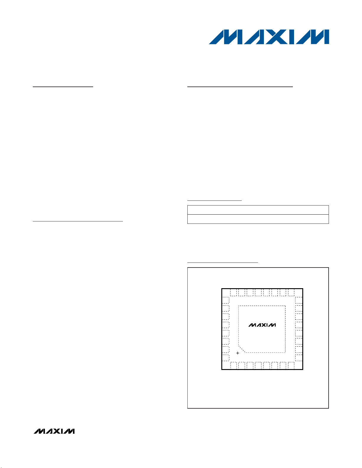
Pin Configuration
MAX4999
TQFN
5mm x 5mm
TOP VIEW
29
30
28
27
12
11
13
V
CC
COM0
COM1
C0
C1
14
GND
D4_0
GND
V
CC
GND
D3_1
D3_0
12
D6_1
4567
2324 22 20 19 18
D6_0
GND
GND
D1_1
D1_0
GND
EN
D4_1
3
21
31
10
D7_1
D0_1
32
9
D7_0
D0_0
GND
26
15
D2_0
D5_0
25
16
D2_1
C2
GND
8
17
D5_1
*CONNECT EXPOSED PAD TO GND.
*EP
PART TEMP RANGE PIN-PACKAGE
MAX4999ETJ+ -40°C to +85°C 32 TQFN-EP*
Page 2
MAX4999
USB 2.0 Hi-Speed Differential
8:1 Multiplexer
2 _______________________________________________________________________________________
ABSOLUTE MAXIMUM RATINGS
ELECTRICAL CHARACTERISTICS
(V
CC
= +3.0V to +3.6V, TA= -40°C to +85°C, unless otherwise noted. Typical values are at VCC= +3.3V and TA= +25°C.) (Note 3)
Stresses beyond those listed under “Absolute Maximum Ratings” may cause permanent damage to the device. These are stress ratings only, and functional
operation of the device at these or any other conditions beyond those indicated in the operational sections of the specifications is not implied. Exposure to
absolute maximum rating conditions for extended periods may affect device reliability.
(All voltages referenced to GND.)
V
CC
...........................................................................-0.3V to +4V
All Other Pins (Note 1)..............................................-0.3V to +4V
Continuous Current (COM_ to any switch) .......................±60mA
Peak Current (COM_ to any switch) (pulsed at 1ms,
10% duty cycle)..........................................................±120mA
Continuous Power Dissipation (T
A
= +70°C)
32-Lead TQFN (derate 34.5mW/°C above +70°C) ....2759mW
Junction-to-Case Thermal Resistance (θ
JC
) (Note 2)
32-Lead TQFN ............................................................2.0°C/W
Junction-to-Ambient Thermal Resistance (θ
JA
) (Note 2)
32-Lead TQFN .............................................................29°C/W
Operating Temperature Range ...........................-40°C to +85°C
Storage Temperature Range .............................-65°C to +150°C
Lead Temperature (soldering, 10s) .................................+300°C
Note 1: Signals exceeding GND are clamped by internal diodes. Limit forward-diode current to maximum current rating.
Note 2: Package thermal resistances were obtained using the method described in JEDEC specification JESD51-7, using a
four-layer board. For detailed information on package thermal considerations, refer to www.maxim-ic.com/thermal-tutorial
.
POWER SUPPLY
Supply Voltage V
Quiescent Supply Current I
ANALOG SWITCH
On-Resistance R
On-Resistance Match ΔR
On-Resistance Match Between
Channels
Leakage Current COM_, D_0, D_1 I
SWITCH AC PERFORMANCE (Note 4)
Crosstalk V
Off-Isolation V
Bandwidth -3dB BW RL = 45Ω unbalanced (Figure 3) 1200 MHz
On-Capacitance C
Off-Capacitance C
Propagation Delay t
Turn-On Time t
PARAMETER SYMBOL CONDITIONS MIN TYP MAX UNITS
CC
O
ONICOM_
ONSCVCOM_
ΔR
ONBCVCOM_
L
DCT1
OFF
ON
OFF
PD
ON
Charge pump on 5
Charge pump off 1
= ±10mA 6.5 12 Ω
= 1V, TA = +25°C 0.8 Ω
= 1V, TA = +25°C 1 Ω
VCC = +3.6V -1 +1 µA
Any switch to non-paired switch at 500MHz
(Figure 3)
Any switch to non-paired switch at 240MHz
(Figure 3)
f = 1MHz 6
Taken from S11 parameters at f = 240MHz 3.0
f = 1MHz, COM_ 5
Taken from S11 parameters at f = 240MHz 3.0
RL = RS = 50Ω (Figure 2) 300 ps
VD0 or VD1 = +1.5V, RL = 300Ω, CL = 35pF,
= VCC, VIL = 0V (Figure 1)
V
IH
3.0 3.6 V
-30 dB
-27 dB
10 µs
µA
pF
pF
Page 3
MAX4999
USB 2.0 Hi-Speed Differential
8:1 Multiplexer
_______________________________________________________________________________________ 3
Note 3: All units are 100% production tested at TA= +85°C. Limits over the operating temperature range are guaranteed by design
and not production tested.
Note 4: Guaranteed by design.
ELECTRICAL CHARACTERISTICS
(V
CC
= +3.0V to +3.6V, TA= -40°C to +85°C, unless otherwise noted. Typical values are at VCC= +3.3V and TA= +25°C.) (Note 3)
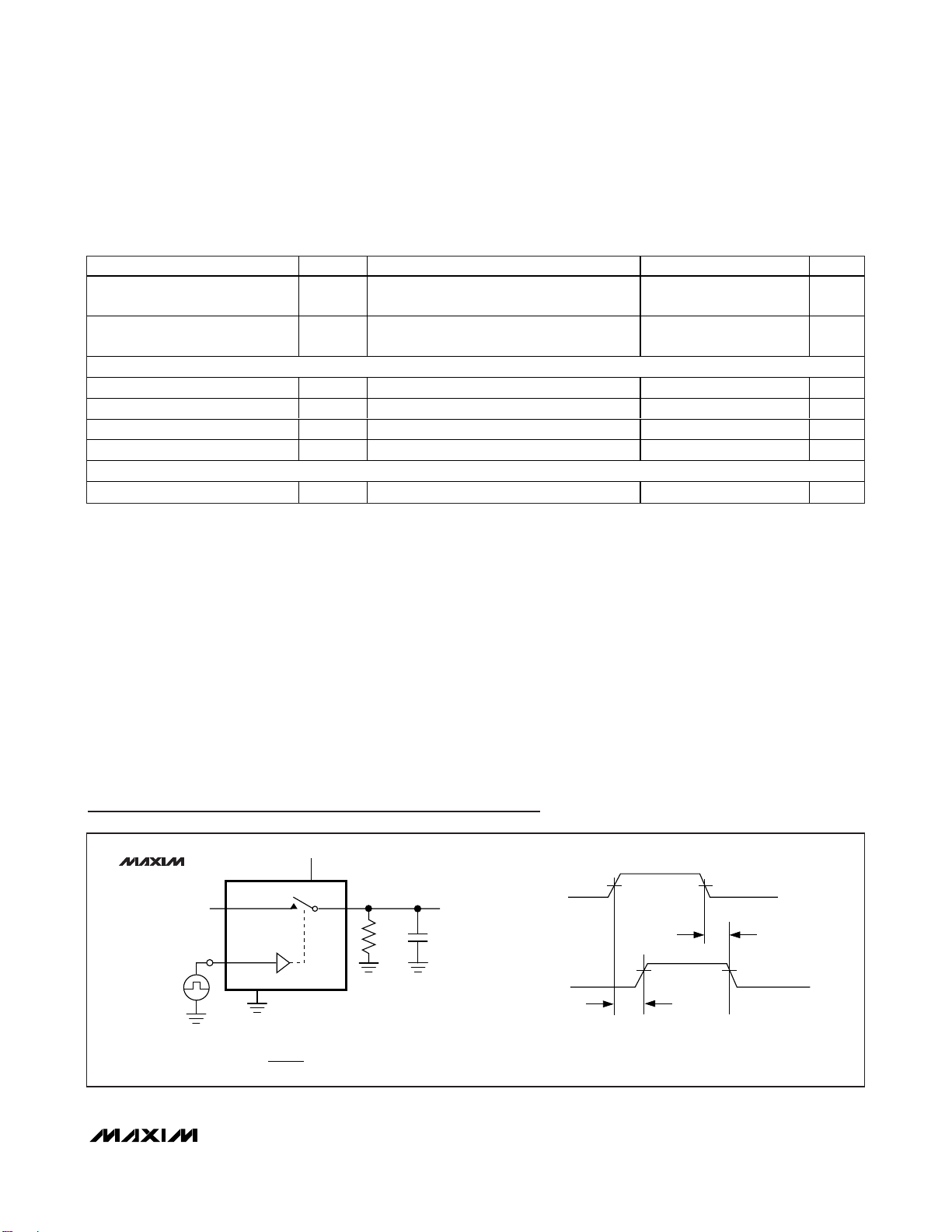
Test Circuits/Timing Diagrams
Figure 1. Switching Time
Turn-Off Time t
Output Skew Same Port t
SWITCH LOGIC
Input Logic Low V
Input Logic High V
Input Logic Hysteresis V
Input Leakage Current I
ESD PROTECTION
All Pins Human Body Model ±2 kV
PARAMETER SYMBOL CONDITIONS MIN TYP MAX UNITS
OFF
PD
IL
IH
HYST
LEAK
VD0 or VD1 = +1.5V, RL = 300Ω, CL = 35pF,
= VCC, VIL = 0V (Figure 1)
V
IH
Skew between any D_0, D_1 line, same port
45Ω unbalanced I/O, f = 240MHz (Figure 2)
VCC = +3.0V 0.6 V
VCC = +3.6V 1.7 V
VCC = +3.6V, V
COM_
= 0V or V
CC
-1 +1 µA
10 µs
30 ps
200 mV
MAX4999
V
N_
LOGIC
INPUT
CL INCLUDES FIXTURE AND STRAY CAPACITANCE.
V
RL + R
D0_
OR D1_
C_
OUT
= V
GND
N_ (
R
V
CC
V
LOGIC
COM_
R
L
L
)
ON
V
OUT
C
L
INPUT
SWITCH
OUTPUT
IH
V
IL
0V
50%
V
OUT
0.9 x V
0UT
t
ON
IN DEPENDS ON SWITCH CONFIGURATION;
INPUT POLARITY DETERMINED BY SENSE OF SWITCH.
tR < 5ns
tF < 5ns
t
OFF
0.9 x V
OUT
Page 4
MAX4999
USB 2.0 Hi-Speed Differential
8:1 Multiplexer
4 _______________________________________________________________________________________
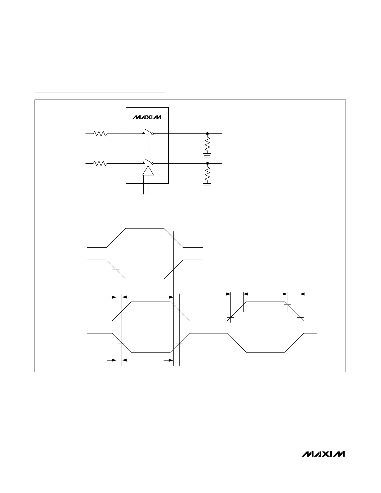
Test Circuits/Timing Diagrams (continued)
Figure 2. Propagation Delay and Skew
IN+
IN-
V
V
IN+
V
IN-
V
V
OUT+
50%
50%
50%
MAX4999
C0C1C
COM1
COM2
2
50%
50%
t
PHL
50%
OUT+
RISE-TIME PROPAGATION DELAY = t
R
L
R
L
FALL-TIME PROPAGATION DELAY = t
tSK = |t
- t
|.
PLH
RS = RL = 50Ω.
OUT-
t
R
10% 10%
PHL
90%
90%
.
PLH
.
PHL
t
F
R
S
D0_1
R
S
D0_0
CC
0V
V+
0V
t
CC
0V
PLH
V
CC
V
OUT-
0V
t
PHL
50%
t
PLH
50%
Page 5
MAX4999
USB 2.0 Hi-Speed Differential
8:1 Multiplexer
_______________________________________________________________________________________ 5
Test Circuits/Timing Diagrams (continued)
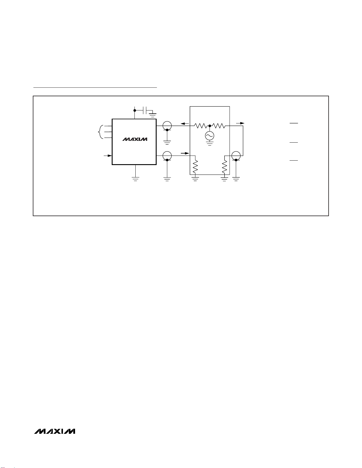
Figure 3. Off-Isolation, On-Loss, and Crosstalk
CHANNEL
SELECT
C0
C1
C2
MAX4999
HIGH
MEASUREMENTS ARE STANDARDIZED AGAINST SHORT AT SOCKET TERMINALS.
OFF-ISOLATION IS MEASURED BETWEEN COM_ AND "OFF" USB_ TERMINAL ON EACH SWITCH.
ON-LOSS IS MEASURED BETWEEN COM_ AND "ON" USB_ TERMINAL ON EACH SWITCH.
CROSSTALK IS MEASURED FROM ONE USB_ CHANNEL TO ANOTHER USB_ CHANNEL.
SIGNAL DIRECTION THROUGH SWITCH IS REVERSED; WORST VALUES ARE RECORDED.
EN
V
V+
GND
0.1μF
CC
NETWORK
D_ _
COM_
V
IN
V
OUT
50Ω
MEAS.
ANALYZER
50Ω
50Ω 50Ω
REF.
OFF-ISOLATION = 20log
ON-LOSS = 20log
CROSSTALK = 20log
V
OUT
V
IN
V
OUT
V
IN
V
OUT
V
IN
Page 6
MAX4999
USB 2.0 Hi-Speed Differential
8:1 Multiplexer
6 _______________________________________________________________________________________
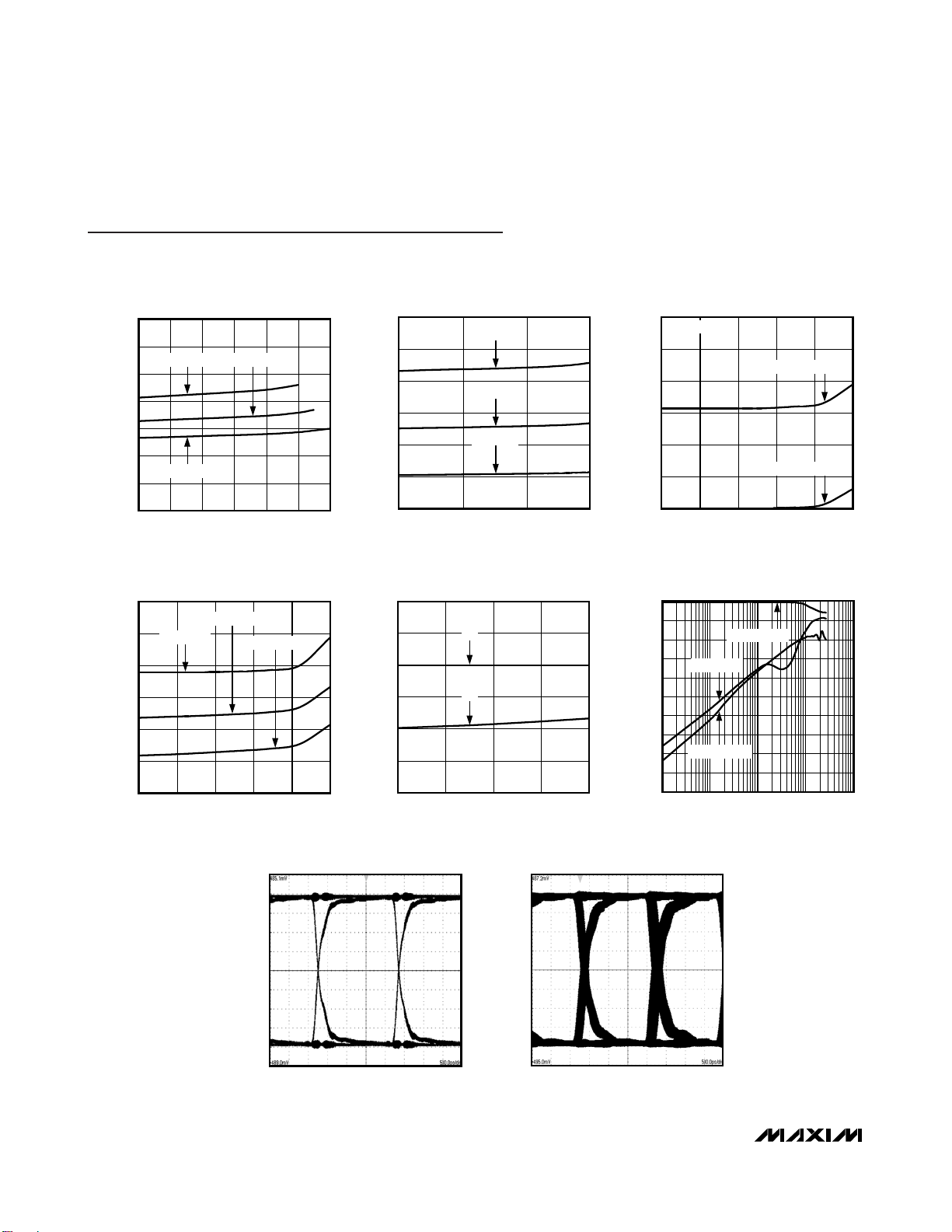
Typical Operating Characteristics
(VCC= +3.3V, TA= +25°C, unless otherwise noted.)
4.6
5.0
4.8
5.4
5.2
5.8
5.6
6.0
0 1.2 1.80.6 2.4 3.0 3.6
ON-RESISTANCE
vs. V
COM
MAX4999 toc01
V
COM
(V)
R
ON
(Ω)
VCC = +3.0V VCC = +3.3V
VCC = +3.6V
4.0
5.0
4.5
6.0
5.5
6.5
7.0
0 1.1 2.2 3.3
ON-RESISTANCE
vs. V
COM
MAX4999 toc02
V
COM
(V)
R
ON
(Ω)
VCC = +3.3V
TA = +85°C
TA = +25°C
TA = -40°C
0
40
20
80
60
100
120
-40 85
LEAKAGE CURRENT
vs. TEMPERATURE
MAX4999 toc03
TEMPERATURE (°C)
LEAKAGE CURRENT (nA)
10-15 35 60
VCC = +3.6V
COM ON-LEAKAGE
COM OFF-LEAKAGE
0.50
0.75
0.63
1.00
0.88
1.13
1.25
-40 85
QUIESCENT SUPPLY CURRENT
vs. TEMPERATURE
MAX4999 toc04
TEMPERATURE (°C)
QUIESCENT SUPPLY CURRENT (μA)
10-15 35 60
VCC = +3.3V
VCC = +3.0V
VCC = +3.6V
0.70
0.80
0.75
0.90
0.85
0.95
1.00
3.0 3.33.2 3.5 3.6
LOGIC THRESHOLD
vs. SUPPLY VOLTAGE
MAX4999 toc05
SUPPLY VOLTAGE (V)
LOGIC THRESHOLD (V)
V
IH
V
IL
0
-100
1 10 100 1000 10,000
FREQUENCY RESPONSE
-80
MAX4999 toc06
FREQUENCY (MHz)
LOSS (dB)
-60
-40
-20
-30
-50
-70
-90
-10
OFF-ISOLATION
ON-RESPONSE
CROSSTALK
EYE DIAGRAM - SINGLE
MAX4999 toc07
EYE DIAGRAM - DOUBLE
MAX4999 toc08
Page 7
MAX4999
USB 2.0 Hi-Speed Differential
8:1 Multiplexer
_______________________________________________________________________________________ 7
Detailed Description
The MAX4999 differential Hi-Speed USB analog multiplexer features low on-capacitance (CON) and low onresistance (RON) necessary for high-performance
switching applications. The low CONis designed for
USB server/mass storage devices. This device is ideal
for USB 2.0 Hi-Speed applications at 480Mbps, while
also meeting the requirements for USB low-/full-speed
applications.
Digital Control Inputs (C0, C1, C2)
The MAX4999 provides three digital control inputs (C0,
C1, C2) to select the analog signal path between the
COM_ and D-/D+ channels. The truth table for the
MAX4999 is shown in the
Functional Diagram/Truth
Table.
Driving the control inputs rail-to-rail minimizes
power consumption.
Enable Input (EN)
The MAX4999 features an enable input that when driven
low, places the device in standby mode. In standby
mode, all channels are high impedance and the internal
charge pump is disabled, thus minimizing the quiescent
supply current. For normal operation, drive EN high.
Analog Signal Levels
Signals applied to COM1 are routed to D_ _1 terminals.
Signals applied to COM0 are routed to D_ _0 terminals.
This multiplexer is bidirectional, allowing COM_ and
D-/D+ terminals to be configured as either inputs or
outputs. Additionally, the MAX4999 can be used for
non-USB signals if the signals fall within the normal
operating range.
The MAX4999 features an internal charge pump that
allows signal levels greater than the supply voltage.
Limit the analog input/output signal level to no more
than the
Absolute Maximum Ratings
.
Pin Description
PIN NAME FUNCTION
1, 11, 14, 17,
21, 24, 27, 30
2, 20 V
3 EN Enable Input
4 COM0 Analog Switch Common D- Terminal
5 COM1 Analog Switch Common D+ Terminal
6 C0 Control Input 0
7 C1 Control Input 1
8 C2 Control Input 2
9 D0_0 Analog Switch 0 D- Terminal
10 D0_1 Analog Switch 0 D+ Terminal
12 D1_0 Analog Switch 1 D- Terminal
13 D1_1 Analog Switch 1 D+ Terminal
15 D2_0 Analog Switch 2 D- Terminal
16 D2_1 Analog Switch 2 D+ Terminal
18 D3_0 Analog Switch 3 D- Terminal
19 D3_1 Analog Switch 3 D+ Terminal
22 D4_1 Analog Switch 4 D+ Terminal
23 D4_0 Analog Switch 4 D- Terminal
25 D5_1 Analog Switch 5 D+ Terminal
26 D5_0 Analog Switch 5 D- Terminal
28 D6_1 Analog Switch 6 D+ Terminal
29 D6_0 Analog Switch 6 D- Terminal
31 D7_1 Analog Switch 7 D+ Terminal
32 D7_0 Analog Switch 7 D- Terminal
— EP Exposed Pad. Connect EP to GND or leave unconnected.
GND Ground
CC
Power-Supply Input. Bypass VCC to GND with a 0.1µF capacitor placed as close to VCC as possible.
Page 8

MAX4999
USB 2.0 Hi-Speed Differential
8:1 Multiplexer
8 _______________________________________________________________________________________
Applications Information
Increasing USB Channels
The MAX4999 features an enable input that allows two
MAX4999s to be connected, allowing multiplexing
between 16 USB channels. Figure 4 shows the typical
application with a single USB common terminal multiplexed to eight channels (8:1). See the Eye Diagram Single graph in the
Typical Operating Characteristics
.
Figure 5 shows two MAX4999 devices configured with
the USB common terminal multiplexed to 16 USB channels (16:1). See the Eye Diagram - Double graph in the
Typical Operating Characteristics
. The MAX4999 was
designed to be symmetrical so that the two common
ports may be wired in parallel with very short wiring to
create a 16:1 configuration. When operating in 16:1 configuration, interchange COM0 and COM1 on the second
device to reverse the D+ and D- pins. This minimizes
vias and crossovers (Figure 5).
USB Switching
The MAX4999 analog multiplexers are fully compliant
with the USB 2.0 specification. The low on-resistance
and low on-capacitance of the MAX4999 make it ideal
for high-performance switching applications.
Board Layout
Hi-Speed switches require proper layout and design procedures for optimum performance. Keep design-controlled impedance PCB traces as short as possible.
Ensure that high-quality bypass ceramic capacitors
(X7R, X5R or better) are placed as close to the device as
possible and use large ground planes where possible.
V
CC
GND
C0
EN
C1
C2
CONTROL
LOGIC
CHARGE
PUMP
MAX4999
COM1
MUX
D0 _1
D1 _1
D2 _1
D3 _1
D4 _1
D5 _1
D6 _1
D7 _1
COM0
MUX
D0 _0
D1 _0
D2 _0
D3 _0
D4 _0
D5 _0
D6 _0
D7 _0
Functional Diagram/Truth Table
X = DON’T CARE
MAX4999
EN C2 C1 C0 FUNCTION
1 0 0 0 COM_→ D0
1 0 0 1 COM_→ D1
1 0 1 0 COM_→ D2
1 0 1 1 COM_→ D3
1 1 0 0 COM_→ D4
1 1 0 1 COM_→ D5
1 1 1 0 COM_→ D6
1 1 1 1 COM_→ D7
0XXX
STANDBY MODE.
ALL SWITCHES IN HIGHIMPEDANCE STATE.
CHARGE PUMP IS OFF.
Page 9

MAX4999
USB 2.0 Hi-Speed Differential
8:1 Multiplexer
_______________________________________________________________________________________ 9
Figure 4. The MAX4999 Multiplexes Between Eight Differential Channels (8:1)
Figure 5. Combining Two MAX4999 Devices for 16:1 USB Connections
+
-
MAX4999
D4_0
USB3
+
-
D3_1
D3_0
1, 11, 14, 17,
21, 24, 27, 30
GND
USB5
USB6
USB7
+
-
+
-
+
-
+3.3V
D5_1
D5_0
D6_1
D6_0
D7_1
D7_0
V
CC
25
26
28
29
31
32
2, 20
COMMON
USB4
D4_1
23 22 19 18
453 678
EN C0 C1 C2
+
-
D2_1
16
15
D2_0
D1_1
13
12
D1_0
D0_1
10
9
D0_0
+
-
+
-
+
-
USB2
USB1
USB0
ONE PAIR SHOWN
+
-
D20
16 15
MAX4999
DEVICE 0
USB D+, D- MUST BE REVERSED IF DEVICES ARE CONNECTED AS SHOWN,
THIS IS TRUE OF D0–D7. C0, C1, C2 ARE CONNECTED IN PARALLEL.
EN0 AND EN1 ARE USED TO SELECT BETWEEN DEVICE 0 AND DEVICE 1.
C2 C1 C0 EN0 EN1
8
7
6
5
4
3
1
+
USB TYPE A
COMMON
+
1
3
4
5
6
7
8
MAX4999
DEVICE 1
15 16
D20
+
-
Page 10

MAX4999
USB 2.0 Hi-Speed Differential
8:1 Multiplexer
Maxim cannot assume responsibility for use of any circuitry other than circuitry entirely embodied in a Maxim product. No circuit patent licenses are
implied. Maxim reserves the right to change the circuitry and specifications without notice at any time.
10
____________________Maxim Integrated Products, 120 San Gabriel Drive, Sunnyvale, CA 94086 408-737-7600
© 2008 Maxim Integrated Products is a registered trademark of Maxim Integrated Products, Inc.
SPRINGER
Package Information
For the latest package outline information, go to
www.maxim-ic.com/packages
.
PACKAGE TYPE PACKAGE CODE DOCUMENT NO.
32 TQFN-EP T3255-4
21-0140
Chip Information
PROCESS: CMOS
 Loading...