

Page 1
General Description
The MAX4996/MAX4996L triple DPDT analog switches
operate from a single +2.5V to +5.5V supply, and feature 2.0Ω (typ) on-resistance, low 6pF (typ) on-capacitance, and low power-supply current consumption. The
MAX4996/MAX4996L combine the low capacitance and
low resistance necessary for high-frequency switching
applications in portable electronics.
The MAX4996/MAX4996L have three logic inputs to
control the switches in pairs. The MAX4996 has an
active-high enable input (EN) to disable the switches,
while the MAX4996L has an active-low enable input
(EN) to disable the switches. The enable input decreas-
es the supply current and also places the COM_ outputs in a high-impedance state.
The MAX4996/MAX4996L feature a 5µA (max) supplycurrent consumption when the logic inputs are not
rail-to-rail. This feature is especially valuable in applications where direct interface to low-voltage processors
is necessary.
The MAX4996/MAX4996L are available in a spacesaving 24-pin (3.5mm x 3.5mm) TQFN package and
operate over the -40°C to +85°C temperature range.
Applications
SD Card Switching
USB Signal Switching
UART Signal Switching
Cell Phones
PDAs
GPS
Portable Media Players (PMP)
Features
♦ Multiplex SD2.0/SDIO Interfaces
♦ Low Power Consumption (2µA max)
♦ +2.5V to +5.5V Supply Voltage Range
♦ Rail-to-Rail Signal Handling
♦ Low-Capacitance Switches, 6pF (typ)
♦ Low On-Resistance, 2Ω (typ)
♦ Excellent On-Resistance Flatness Over the Range
of 0V to V
CC
♦ Wide -3dB Bandwidth, 670MHz
♦ Small 24-Pin TQFN (3.5mm x 3.5mm)
MAX4996/MAX4996L
Triple DPDT, Low-Capacitance Data Switches
________________________________________________________________
Maxim Integrated Products
1
Ordering Information
19-4036; Rev 0; 2/08
For pricing, delivery, and ordering information, please contact Maxim Direct at 1-888-629-4642,
or visit Maxim’s website at www.maxim-ic.com.
Typical Operating Circuit appears at end of data sheet.
PART
PINPACKAGE
PAC KA GE
CODE
MAX4996ETG+ 24 TQFN-EP* T243A3-1
M A X4 9 9 6 L E TG+ 24 TQFN-EP* T243A3-1
Note: All devices operate over the -40°C to +85°C extended
temperature range.
+Denotes a lead-free package.
*
EP = Exposed paddle.
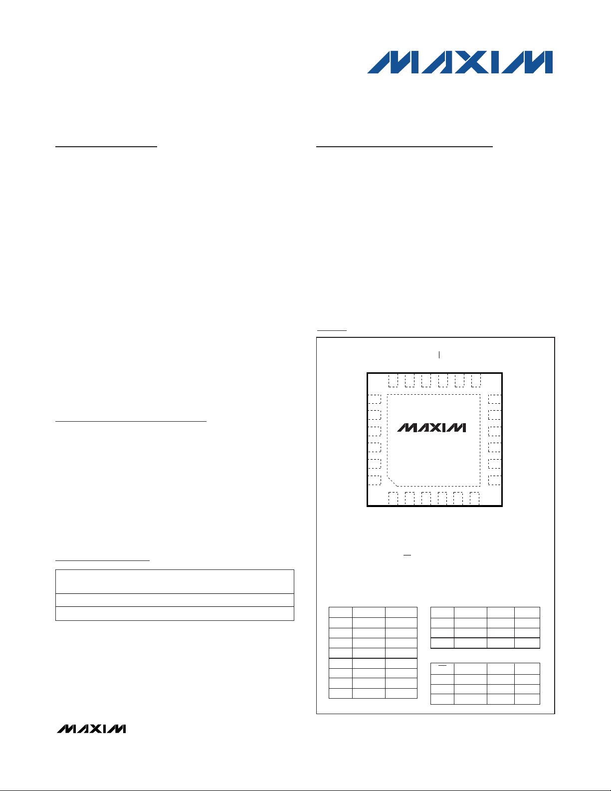
Pin Configuration/Truth Tables
TOP VIEW
COM1
COM2
18
17
NO1
19
*EP
20
NO2
21
NO3
NO4
22
23
NO5
24
NO6
+
*CONNECT EXPOSED PADDLE TO GROUND.
MAX4996
MAX4996L
1
2
CB12
CB34
3.5mm x 3.5mm
(EN) FOR MAX4996L ONLY.
COM3
16
3
CB56
TQFN
EN (EN)
15
4
COM4
CC
V
14
5
COM5
GND
13
6
COM6
NC1
12
11
NC2
10
NC3
9
NC4
8
NC5
7
NC6
MAX4996/MAX4996L
OFF
ON
OFF
ON
OFF
ON
NC1/NC2
ON
OFF
ON
OFF
NC5/NC6
ON
OFF
NO1/NO2
CB12
LOW
HIGH
NO3/NO4 NC3/NC4
CB34
LOW
HIGH
CB56
NO5/NO6
LOW
HIGH
TRUTH TABLES
MAX4996
EN
CB_
HIGH
LOW
HIGH
HIGH
LOW X OFF OFF
MAX4996L
EN
CB_
LOW
LOW
LOW
HIGH
HIGH X OFF OFF
NO_
OFF
ON
NO_
OFF
ON
NC_
ON
OFF
NC_
ON
OFF
Page 2
MAX4996/MAX4996L
Triple DPDT, Low-Capacitance Data Switches
2 _______________________________________________________________________________________
ABSOLUTE MAXIMUM RATINGS
ELECTRICAL CHARACTERISTICS
(VCC= +2.5V to +5.5V, TA= -40°C to +85°C, unless otherwise noted. Typical values are at VCC= 2.8V, TA= +25°C.) (Notes 2, 3)
Stresses beyond those listed under “Absolute Maximum Ratings” may cause permanent damage to the device. These are stress ratings only, and functional
operation of the device at these or any other conditions beyond those indicated in the operational sections of the specifications is not implied. Exposure to
absolute maximum rating conditions for extended periods may affect device reliability.
Note 1: Package thermal resistances were obtained using the method described in JEDEC specification JESD51-7, using a four-
layer board. For detailed information on package thermal considerations see www.maxim-ic.com/thermal-tutorial
.
V
CC
to GND ...........................................................-0.3V to +6.0V
EN, EN, CB_ ..........................................................-0.3V to +6.0V
All Other Pins to GND ..................................-0.3V to V
CC
+ 0.3V
Continuous Current
NO_, NC_, COM_ .......................................................±150mA
Peak Current NO_, NC_, COM_
(pulsed at 1ms, 50% Duty Cycle)...............................±300mA
(pulsed at 1ms, 10% Duty Cycle)...............................±450mA
ESD per Human Body Model...............................................±2kV
Continuous Power Dissipation (T
A
= +70°C)
24-Pin TQFN (derate 20.8mW/°C
above +70°C).............................................................1228mW
Thermal Resistance (Note 1)
θ
JA
.............................................................................65.1°C/W
θ
JC
...............................................................................5.4°C/W
Operating Temperature Range ...........................-40°C to +85°C
Junction Temperature......................................................+150°C
Storage Temperature Range .............................-65°C to +150°C
Lead Temperature (soldering) .........................................+300°C
)
ANALOG SWITCH
Analog Signal Range
On-Resistance R
On-Resistance Match Between
Channels
On-Resistance Flatness R
Off-Leakage Current
On-Leakage Current I
-3dB Bandwidth BW RL = RS = 50Ω, CL = 5pF, Figure 4 670 MHz
Off-Isolation V
C r osstal kV
LOGIC INPUTS
Input Logic High V
Input Logic Low V
Input Leakage Current I
PARAMETER SYMBOL CONDITIONS MIN TYP MAX UNITS
V
,
COM
, VNC_
V
NO
V
ON
ΔR
ON
FLAT
I
_
COM
(OFF)
COM_ (ON
_= 0 to V
C OM
VCC = 2.8V, I
V
= 1.5V or V
NO_
VCC = 2.5V, I
V
_= 0 to V
COM
VCC = 4V , V
V
, V
N O_
N C
VCC = 5.5V , V
V
, V
N O
N C
VCC = 5.5V , V
V
_, V
N O
N C
, I
C C
COM
COM
C OM
_= 25m A24Ω
C OM
_= 25mA;
= 1.5V (Note 4)
NC _
_= 25mA;
(Note 5)
CC
_ = 0, 4V ;
_ = 4V , 0
_ = 5.5V ;
C OM
w i th 50µA sink cur r ent to GN D
_ = 0, 5.5V ;
C OM
_unconnected
f = 1MHz, VNO_, VNC_ = 0;
= 5pF, RL = RS = 50Ω,
C
ISO
L
Figure 4 (Note 6)
CT
LEAK
f = 1MHz, VNO_, VNC_ = 0;
= RS = 50Ω, Figure 4 ( N ote 7)
R
L
IH
IL
0 ≤ V ≤ VIL and VIH ≤ V ≤ VCC;
V
= 5.5V
CC
0V
CC
0.1 0.2 Ω
0.2 0.5 Ω
-250 +250 nA
180 µA
-250 +250 nA
-60 dB
-120 dB
1.4 V
0.5 V
-250 +250 nA
V
Page 3
MAX4996/MAX4996L
Triple DPDT, Low-Capacitance Data Switches
_______________________________________________________________________________________ 3
Note 2: The algebraic convention is used. The most negative value is shown in the minimum column.
Note 3: Parts are 100% tested at T
A
= +25°C. Limits across the full temperature range are guaranteed by correlation and design.
Note 4: ΔR
ON
= R
ON(MAX)
- R
ON(MIN)
.
Note 5: Flatness is defined as the difference between the maximum and minimum value of on-resistance as measured over the
specified analog signal ranges.
Note 6: Off-isolation = 20log
10[VCOM_
/ (V
NO_
or V
NC_
)], V
COM_
= output, V
NO_
or V
NC_
= input to off switch.
Note 7: Between any two switches.
)
)
ELECTRICAL CHARACTERISTICS (continued)
(VCC= +2.5V to +5.5V, TA= -40°C to +85°C, unless otherwise noted. Typical values are at VCC= 2.8V, TA= +25°C.) (Notes 2, 3)
PARAMETER SYMBOL CONDITIONS MIN TYP MAX UNITS
SWITCH DYNAMICS
Turn-On Time t
Turn-Off Time t
Break-Before-Make Interval t
Output Skew Between Switches t
C
NO or NC Off-Capacitance
COM Off-Capacitance
COM On-Capacitance
NO_ (OFF
CNC_
C
C
Operating Power-Supply Range V
Shutdown S up p l y C ur r ent
VCC S up p l y C ur rent I
Increase in Supply Current with
/ VEN Voltage
V
CB
ON
OFF
BBM
SKEW
COM
(OFF)
COM
(ON)
CC
CC
VCC = 2.7V, VNO_ or VNC_ = 1.5V;
= 50Ω, CL = 35pF, Figure 1
R
L
VCC = 2.7V, VNO_ or VNC_ = 1.5V;
= 50Ω, CL = 35pF, Figure 1
R
L
VCC = 2.7V ; VNO_, or VNC_ = 1.5V;
= 50Ω, CL = 35pF, Figure 2
R
L
10 µs
RL = RS = 50Ω, Figure 3 40 Ps
(OFF
_
_
f = 10MHz, V
signal = 500mV
f = 10MHz, V
signal = 500mV
f = 10MHz, V
signal = 500mV
BIAS
BIAS
BIAS
= 0V,
, Figure 5
P-P
= 0V,
, Figure 5
P-P
= 0V,
, Figure 5
P-P
2.5 pF
4pF
6pF
2.5 5.5 V
V
= 0 (MAX4996), VEN = V
EN
(MAX4996L)
VCB_ = 0 or VCC;
V
= VCC (MAX4996);
EN
= 0 (MAX4996L)
V
EN
0 ≤ V
_ ≤ VIL or VIH ≤ VCB_ ≤ V
CB
or 0 ≤ V
≤ VIL or VIH ≤ V
EN
CC
VCC = 2.8V 1 2
= 5.5V 5 10
V
CC
CC
≤ V
EN
CC
0.1 0.5 µA
ESD Protection Human Body Model ±2 kV
100 µs
6µs
5µA
µA
Page 4
MAX4996/MAX4996L
Triple DPDT, Low-Capacitance Data Switches
4 _______________________________________________________________________________________
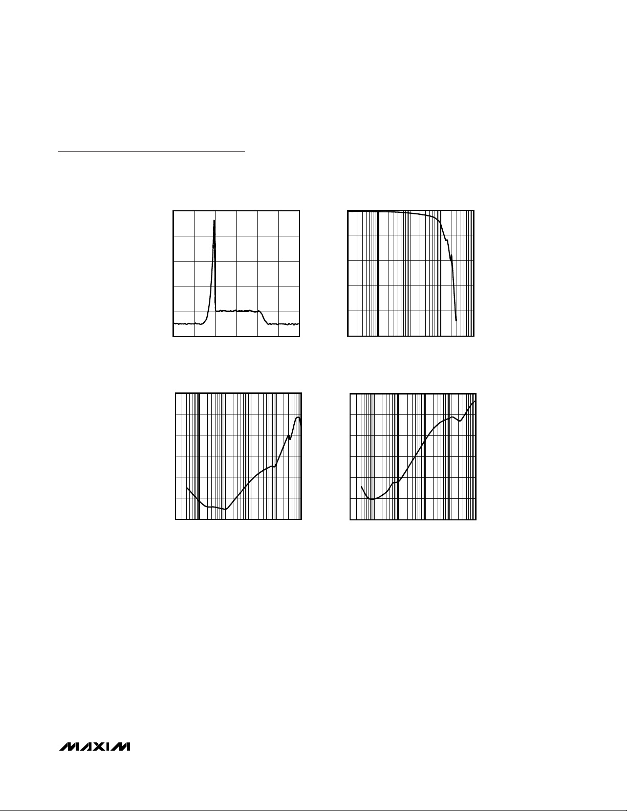
Typical Operating Characteristics
(VCC= 3V, TA= +25°C, unless otherwise noted.)
3.0
2.5
(Ω)
ON
R
VCC = 2.5V
2.0
VCC = 3.0V
1.5
VCC = 5.0V
1.0
053142
V
COM
ON-RESISTANCE vs. V
VCC = 2.7V
(V)
COM
MAX4996/6L toc01
3.0
2.5
(Ω)
2.0
ON
R
1.5
1.0
COM_ON LEAKAGE CURRENT
vs. OVERTEMPERATURE
45
40
35
30
(nA)
25
20
COM_ON
I
15
10
5
0
TA = -40°C TO +85°C
0231
V
(V)
COM
ON-RESISTANCE vs. V
0231
TA = +85°C
= +25°C
T
A
T
= -40°C
A
V
COM
MAX4996/6L toc04
COM
(V)
MAX4996/6L toc02
(Ω)
R
2.0
1.5
1.0
ON
0.5
0
SUPPLY CURRENT vs. SUPPLY VOLTAGE
5
4
3
(μA)
CC
I
2
1
0
0462
VCC (V)
ON-RESISTANCE vs. V
VCC = 5.0V
053142
MAX4996/6L toc05
TA = +85°C
TA = +25°C
TA = -40°C
V
(V)
COM
COM
MAX4996/6L toc03
QUIESCENT SUPPLY CURRENT
3.5
vs. TEMPERATURE
3.0
2.5
2.0
(μA)
CC
I
1.5
1.0
0.5
0
-40 10 60-15 35 85
VCC = 5.0V
VCC = 3.0V
TEMPERATURE (°C)
MAX4996/6L toc06
LOGIC THRESHOLD vs. SUPPLY VOLTAGE
2.0
1.5
V
IH
1.0
THRESHOLD (V)
0.5
0
1.5 2.5 3.5 4.5 5.52.0 3.0 4.0 5.0 6.0
VCC (V)
V
IL
MAX4996/6L toc07
Page 5
MAX4996/MAX4996L
Triple DPDT, Low-Capacitance Data Switches
_______________________________________________________________________________________
5
Typical Operating Characteristics (continued)
(VCC= 3V, TA= +25°C, unless otherwise noted.)
QUIESCENT SUPPLY CURRENT
vs. LOGIC LEVEL
10
8
6
(μA)
CC
I
4
2
0
0 1.00.5 1.5 2.0 2.5 3.0
VCB (V)
INPUT CROSSTALK
FREQUENCY RESPONSE
0
-20
-40
INPUT ON-LOSS
FREQUENCY RESPONSE
MAX4996/6L toc09
1 10010 1,000 10,000
FREQUENCY (MHz)
INPUT OFF-ISOLATION
FREQUENCY RESPONSE
MAX4996/6L toc11
MAX4996/6L toc08
MAX4996/6L toc10
0
0
-5
-10
-15
ON-LOSS (dB)
-20
-25
0
-20
-40
-60
ON-LOSS (dB)
-80
-100
-120
0.01 0.1 1 10 100 1,000
FREQUENCY (MHz)
-60
ON-LOSS (dB)
-80
-100
-120
0.01 0.1 1 10 100 1,000
FREQUENCY (MHz)
Page 6

MAX4996/MAX4996L
Triple DPDT, Low-Capacitance Data Switches
6 _______________________________________________________________________________________
Pin Description
PIN NAME FUNCTION
1 CB12
2 CB34
3 CB56
4 COM4 Analog Switch 4—Common Terminal
5 COM5 Analog Switch 5—Common Terminal
6 COM6 Analog Switch 6—Common Terminal
7 NC6 Analog Switch 6—Normally Closed Terminal
8 NC5 Analog Switch 5—Normally Closed Terminal
9 NC4 Analog Switch 4—Normally Closed Terminal
10 NC3 Analog Switch 3—Normally Closed Terminal
11 NC2 Analog Switch 2—Normally Closed Terminal
12 NC1 Analog Switch 1—Normally Closed Terminal
13 GND Ground
14 V
15 EN, EN
16 COM3 Analog Switch 3—Common Terminal
17 COM2 Analog Switch 2—Common Terminal
18 COM1 Analog Switch 1—Common Terminal
19 NO1 Analog Switch 1—Normally Open Terminal
20 NO2 Analog Switch 2—Normally Open Terminal
21 NO3 Analog Switch 3—Normally Open Terminal
22 NO4 Analog Switch 4—Normally Open Terminal
23 NO5 Analog Switch 5—Normally Open Terminal
24 NO6 Analog Switch 6—Normally Open Terminal
—EP
Digital Control Input for Analog Switches 1 and 2. Drive CB12 low to connect COM1 to NC1 and COM2 to
NC2. Drive CB12 high to connect COM1 to NO1 and COM2 to NO2.
Digital Control Input for Analog Switches 3 and 4. Drive CB34 low to connect COM3 to NC3 and COM4 to
NC4. Drive CB34 high to connect COM3 to NO3 and COM4 to NO4.
Digital Control Input for Analog Switches 5 and 6. Drive CB56 low to connect COM5 to NC5 and COM6 to
NC6. Drive CB56 high to connect COM5 to NO5 and COM6 to NO6.
P osi ti ve S up p l y V ol tag e. Byp ass V
CC
Enable Logic Input. For the MAX4996, drive EN high to enable all the switches. Drive EN low to disable all
switches. For the MAX4996L, drive EN low to enable all the switches. Drive EN high to disable all switches.
COM_ is high impedance when the switch is disabled. (See Pin Configuration/Truth Tables.)
Exposed Paddle. Internally connected to GND. Connect to a large ground plane to maximize thermal
performance; not intended as an electrical connection point.
to G N D w i th a 0.1µF cer am i c cap aci tor as cl ose as p ossi b l e to the d evi ce.
C C
Page 7

MAX4996/MAX4996L
Triple DPDT, Low-Capacitance Data Switches
_______________________________________________________________________________________ 7
Timing Circuits/Timing Diagrams
Figure 1. Switching Time
Figure 2. Break-Before-Make Interval
MAX4996
MAX4996L
V
IN
LOGIC
INPUT
MAX4996
MAX4996L
V
IN
LOGIC
INPUT
NO_
OR NC_
CB_
INCLUDES FIXTURE AND STRAY CAPACITANCE.
C
L
V
RL + R
R
= V
OUT
IN (
NC_
NO_
CB_
CL INCLUDES FIXTURE AND STRAY CAPACITANCE.
COM_
R
L
)
ON
COM_
V
CC
LOGIC
INPUT
V
OUT
L
C
L
SWITCH
OUTPUT
V
OUT
R
L
C
L
0V
0V
LOGIC
INPUT
V
OUT
50%
V
OUT
0.9 x V
0UT
t
ON
V
CC
0V
50%
t
BBM
tr < 5ns
tf < 5ns
50%
t
OFF
0.9 x V
OUT
0.9 x V
OUT
Page 8
MAX4996/MAX4996L
Triple DPDT, Low-Capacitance Data Switches
8 _______________________________________________________________________________________
Figure 3. Input/Output Skew Timing Diagram
Timing Circuits/Timing Diagrams (continued)
MAX4996/
NC OR
R
S
V
IN+
V
IN-
NO_
NC OR
R
S
NO_
MAX4996L
CB
VIL TO V
COM_
COM_
IH
t
SKEW
= |t
PLHX
V
OUT+
R
L
V
OUT-
R
L
- t
| OR |t
- t
PHLX
PHLY
|
PLHY
V
CC
V
IN+
0V
V
CC
V
IN-
0V
t
PLHX
CC
0V
CC
0V
t
PHLY
V
V
V
OUT+
V
OUT-
50%
50%
50%
50%
t
PHLX
t
PLHY
50%
50%
50%
50%
Page 9

MAX4996/MAX4996L
Triple DPDT, Low-Capacitance Data Switches
_______________________________________________________________________________________ 9
Figure 4. On-Loss, Off-Isolation, and Crosstalk
Figure 5. Channel On-/Off-Capacitance
Timing Circuits/Timing Diagrams (continued)
0 OR V
50Ω
MEASUREMENTS ARE STANDARDIZED AGAINST SHORTS AT IC TERMINALS.
OFF-ISOLATION IS MEASURED BETWEEN COM_ AND OFF NO_ OR NC_ TERMINAL ON EACH SWITCH.
ON-LOSS IS MEASURED BETWEEN COM_ AND ON NO_ OR NC_ TERMINAL ON EACH SWITCH.
CROSSTALK IS MEASURED FROM ONE CHANNEL TO THE OTHER CHANNEL.
SIGNAL DIRECTION THROUGH SWITCH IS REVERSED; WORST VALUES ARE RECORDED.
CB_
CC
NC1
MAX4996
MAX4996L
COM1
NO1*
CAPACITANCE
METER
f = 10MHz
V
NETWORK
ANALYZER
V
IN
V
OUT
50Ω
MEAS REF
50Ω 50Ω
COM_
50Ω
MAX4996
OFF-ISOLATION = 20log ✕
ON-LOSS = 20log ✕
CROSSTALK = 20log ✕
*FOR CROSSTALK THIS PIN IS NO2.
NC2 AND COM2 ARE OPEN.
MAX4996L
CB_
V
OR V
IL
IH
NC_ or
NO_
OUT
V
IN
V
OUT
V
IN
V
OUT
V
IN
Page 10
MAX4996/MAX4996L
Triple DPDT, Low-Capacitance Data Switches
10 ______________________________________________________________________________________
Detailed Description
The MAX4996/MAX4996L triple DPDT analog switches
operate from a single +2.5V to +5.5V supply and feature
2.0Ω (typ) on-resistance, low 6pF (typ) on-capacitance,
and low power-supply current consumption. The combination of low resistance and low capacitance make this
switch ideal for high-frequency applications.
The MAX4996 has an active-high enable input (EN) to
disable the switches, while the MAX4996L has an
active-low enable input (EN) to disable the switches.
The enable input decreases the supply current and also
places the COM_ outputs in a high-impedance state.
Digital Control Inputs
Each pair of switches feature a digital-control logic
input: CB_. CB_ controls the position of the switches as
shown in the
Pin Configuration/Truth Tables
. The
MAX4996/MAX4996L also feature an enable input to
turn all switches on or off. Drive EN low on the
MAX4996, or EN high on the MAX4996L, to disable the
switches. While disabled, the switches are high-impedance and the supply current drops to 0.1µA (typ). To
enable all switches, drive EN high on the MAX4996 or
EN low on the MAX4996L.
Driving all digital inputs (CB_, EN, EN) rail-to-rail minimizes supply current.
Analog Signal Levels
The on-resistance of the MAX4996/MAX4996L are very
low and stable as the analog input signals are swept
from ground to VCC(see the
Typical Operating
Characteristics
). These switches are bidirectional,
allowing NO_, NC_, and COM_ to be configured as
either inputs or outputs.
Applications Information
Power-Supply Bypassing
Power-supply bypassing improves noise margin and
prevents switching noise from propagating from the
V
CC
supply to other components. A 0.1µF ceramic
capacitor connected from VCCto GND is adequate for
most applications.
Power-Supply Sequencing
Always apply VCCbefore the analog signals.
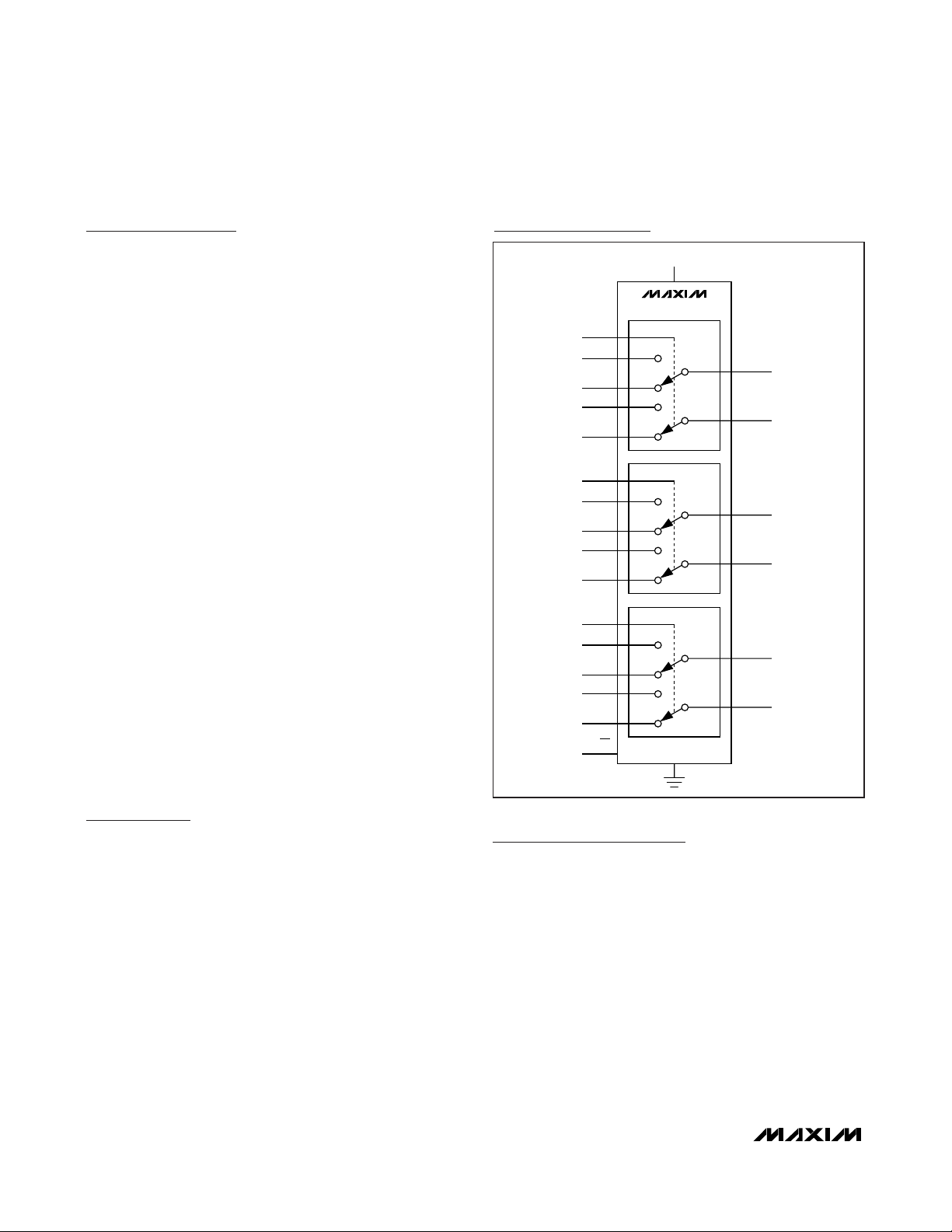
Chip Information
PROCESS: BiCMOS
Functional Diagram
CB12
NO1
NC1
NO2
NC2
CB34
NO3
NC3
NO4
NC4
CB56
NO5
NC5
NO6
NC6
EN (EN)
V
CC
MAX4996/MAX4996L
COM1
COM2
COM3
COM4
COM5
COM6
GND
Page 11
MAX4996/MAX4996L
Triple DPDT, Low-Capacitance Data Switches
______________________________________________________________________________________ 11
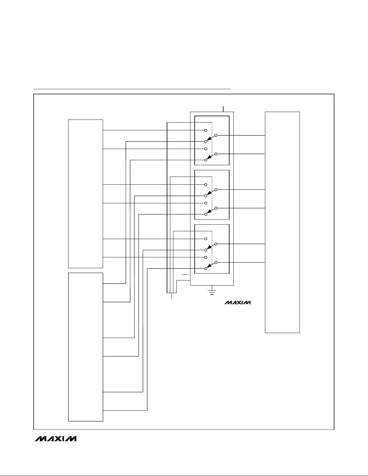
Typical Operating Circuit
BASEBAND
SD CARD
INTERFACE
CLK
CMD
DAT0
DAT1
DAT2
DAT3
CB12
NO1
NC1
NO2
NC2
CB34
NO3
NC3
NO4
NC4
CB56
NO5
NC5
NO6
NC6
V
CC
COM1
COM2
COM3
COM4
COM5
COM6
SD CARD
EN (EN)
GND
MAX4996/
MAX4996L
APPLICATION
PROCESSOR
SD CARD
INTERFACE
CLK
CMD
DAT0
DAT1
DAT2
DAT3
DIGITAL CONTROL
FROM BASEBAND
Page 12

MAX4996/MAX4996L
Triple DPDT, Low-Capacitance Data Switches
12 ______________________________________________________________________________________
Package Information
(The package drawing(s) in this data sheet may not reflect the most current specifications. For the latest package outline information
go to www.maxim-ic.com/packages
.)
24L THIN QFN.EPS
Page 13

MAX4996/MAX4996L
Triple DPDT, Low-Capacitance Data Switches
Maxim cannot assume responsibility for use of any circuitry other than circuitry entirely embodied in a Maxim product. No circuit patent licenses are
implied. Maxim reserves the right to change the circuitry and specifications without notice at any time.
Maxim Integrated Products, 120 San Gabriel Drive, Sunnyvale, CA 94086 408-737-7600 ____________________
13
© 2008 Maxim Integrated Products is a registered trademark of Maxim Integrated Products, Inc.
Package Information (continued)
(The package drawing(s) in this data sheet may not reflect the most current specifications. For the latest package outline information
go to www.maxim-ic.com/packages
.)
 Loading...