

General Description
The MAX4991–MAX4994 low on-resistance analog
switches operate from a single +1.8V to +5.5V supply.
The MAX4991/MAX4993 feature a slow turn-on time to
reduce clicks and pops due to coupling capacitors and
audio amplifiers with a DC output bias. This feature provides click-and-pop reduction without adding additional
parts for existing architectures.
The MAX4991/MAX4992 are dual single-pole/doublethrow (SPDT) switches, while the MAX4993/MAX4994
are double-pole/double-throw (DPDT) switches. The
MAX4993/MAX4994 feature an active-low enable input
(EN) that sets all the channels to high impedance and
reduces supply current when driven high. These
devices have 0.3Ω on-resistance and 0.004% THD+N
to route high fidelity audio signals.
The MAX4991–MAX4994 are available in space-saving
10-pin UTQFN (1.4mm x 1.8mm) package, and are
specified for operation over the -40°C to +85°C extended temperature range.
Applications
Speaker Headset Source Switching
Cellular Phones
Portable MP3 Players
Audio Signal Routing
Features
♦ Slow Turn-On for Click-and-Pop Reduction Without
Additional Parts
♦ Low 0.3Ω On-Resistance
♦ Low R
ON
Flatness (1mΩ)
♦ Low THD+N: 0.004%
♦ +1.8V to +5.5V Single-Supply Operation
♦ 1.2µA (typ) Supply Current
♦ Space-Saving Packages
10-Pin UTQFN (1.4mm x 1.8mm x 0.55mm)
MAX4991–MAX4994
Low R
ON
, Dual-SPDT/Single-DPDT Analog
Switches with Slow Turn-On Time
________________________________________________________________
Maxim Integrated Products
1
Ordering Information/Selector Guide
19-4150; Rev 1; 6/09
For pricing, delivery, and ordering information, please contact Maxim Direct at 1-888-629-4642,
or visit Maxim’s website at www.maxim-ic.com.
Note: All devices operate over -40°C to +85°C extended temperature range.
+
Denotes a lead(Pb)-free/RoHS-compliant package.
*
Future product—contact factory for availability.
Typical Application Circuit appears at end of data sheet.
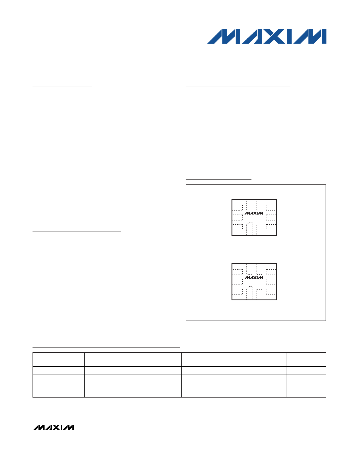
Pin Configurations
TOP VIEW
CB2
COM2
NO2
COM2
NO2
8
9
10
8
EN
9
10
NC2
7 6
MAX4991/
MAX4992
1 2
CC
V
UTQFN
NC2
7 6
MAX4993/
MAX4994
1 2
CC
V
UTQFN
GND
NO1
GND
NO1
5
NC1
4
CB1
3
COM1
5
NC1
4
CB
3
COM1
PART PIN-PACKAGE CONFIGURATION
MAX4991EVB+* 10 UTQFN Dual SPDT Yes No AAD
MAX4992EVB+ 10 UTQFN Dual SPDT No No AAE
MAX4993EVB+ 10 UTQFN DPDT Yes Yes AAF
MAX4994EVB+* 10 UTQFN DPDT No Yes AAG
SLOW-SWITCHING
TIME
ENABLE LINE
TOP
MARK
MAX4991–MAX4994
Low R
ON
, Dual-SPDT/Single-DPDT Analog
Switches with Slow Turn-On Time
2 _______________________________________________________________________________________
ABSOLUTE MAXIMUM RATINGS
ELECTRICAL CHARACTERISTICS
(VCC= +2.7V to +5.5V, TA= -40°C to +85°C, unless otherwise noted. Typical values are at VCC= +3.0V, TA= +25°C.) (Note 2)
Stresses beyond those listed under “Absolute Maximum Ratings” may cause permanent damage to the device. These are stress ratings only, and functional
operation of the device at these or any other conditions beyond those indicated in the operational sections of the specifications is not implied. Exposure to
absolute maximum rating conditions for extended periods may affect device reliability.
(Voltages referenced to GND.)
V
CC
, CB_, EN ........................................................-0.3V to +6.0V
COM_, NC_, NO_ ...................................... -0.3V to (V
CC
+ 0.3V)
Continuous Current COM_, NC_, NO_ ...........................±350mA
Peak Current COM_, NC_, NO_ (pulsed at 1ms,
50% duty cycle)..........................................................±700mA
Peak Current COM_, NC_, NO_ (pulsed at 1ms,
10% duty cycle)..............................................................±1.5A
Continuous Power Dissipation (T
A
= +70°C)
10-Pin UTQFN (derate 6.9mW/°C above +70°C).........559mW
Junction-to-Case Thermal Resistance (
θ
JC
) (Note 1)
10-Pin UTQFN ...........................................................20.1°C/W
Junction-to-Ambient Thermal Resistance (
θ
JA
) (Note 1)
10-Pin UTQFN .........................................................143.1°C/W
Operating Temperature Range ...........................-40°C to +85°C
Junction Temperature Range ..........................................+150°C
Storage Temperature Range ............................ -65°C to +150°C
Lead Temperature (soldering, 10s) .................................+300°C
Note 1: Package thermal resistances were obtained using the method described in JEDEC specification JESD51-7, using a 4-layer
board. For detailed information on package thermal considerations, refer to www.maxim-ic.com/thermal-tutorial
.
PARAMETER SYMBOL CONDITIONS MIN TYP MAX UNITS
Power-Supply Range V
Undervoltage Lockout V
Supply Current
(MAX4991/MAX4992)
Supply Current
(MAX4993/MAX4994)
Power-Supply Rejection
Ratio
Analog Signal Range
On-Resistance R
On-Resistance Match
Between Channels
On-Resistance Flatness R
COM_ Output Noise N
PSRR R
V
NC_
V
R
CC
UVLO
I
CC
I
CC
, V
COM_
ON
ON
FLAT
COM_
1.8 5.5 V
1.4 V
V
= V
CB1
V
CB1
+1.4V
VEN = VCC, VCB = 0V or VCC VCC = +5.5V 0.1 1
VEN = 0V, VCB = 0V or V
VEN = VCB = +0.5V or +1.4V
= RS = 50, f = 20kHz 80 dB
L
,
NO_
0 VCC V
VCC = +2.7V, V
to V
CC
VCC = +2.7V, between NC_, NO_ only,
I
COM_
VCC = +2.7V, V
I
COM_
V
NC_
= 0V or V
CB2
= V
= +0.5V or
CB2
or V
, I
= 100mA, V
= 100mA (Note 3)
= V
NC_
= 100mA
COM_
NC_
= 0V, RL = 50
NO_
NC_
or V
CC
CC
NO_
or V
NO_
VCC = +3V 1.2 2.5
V
= +5.5V 3.1 6
CC
VCC = +2.7V 3
= +5.5V 14
V
CC
VCC = +3V 1.2 2.5
VCC = +5.5V 3.1 6
VCC = +2.7V 3
= +5.5V 8.5
V
CC
TA = +25°C 0.3 0.5
= 0
T
= T
MIN
to T
MAX
A
= VCC/2
NO_
= 0 to VCC,
f = 20Hz to 20kHz 1
f = 0Hz to 1MHz 50
0.6
3 m
1 m
μV
μA
μA
RMS
MAX4991–MAX4994
Low R
ON
, Dual-SPDT/Single-DPDT Analog
Switches with Slow Turn-On Time
_______________________________________________________________________________________ 3
ELECTRICAL CHARACTERISTICS (continued)
(VCC= +2.7V to +5.5V, TA= -40°C to +85°C, unless otherwise noted. Typical values are at VCC= +3.0V, TA= +25°C.) (Note 2)
Note 2: All devices are 100% production tested at TA= +25°C. All temperature limits are guaranteed by design.
Note 3: Flatness is defined as the difference between the maximum and minimum values of on-resistance as measured over the
specified analog ranges.
Note 4: All timing is measured using 10% and 90% levels.
Note 5: Off-isolation = 20log [V
COM_
/(V
NO_
or V
NC_
)], V
COM_
= output, V
NO_
or V
NC_
= input to off switch.
Note 6: Between any two switches.
PARAMETER SYMBOL CONDITIONS MIN TYP MAX UNITS
NC_, NO_, Off-Leakage
Current
COM_ Off-Leakage Current
(MAX4993/MAX4994)
COM_ On-Leakage Current I
I
L(OFF)
I
COM_L(OFF)
COM_L(ON)
VCC = +2.7V, switch open, V
or V
, V
, V
COM_
COM_
= VCC or 0V
NC_
= VCC or 0V
CC
VCC = +2.7V, VEN = VCC, V
or V
CC
VCC = +2.7V, switch closed, V
V
or unconnected, V
CC
= 0V, VCC, or
COM_
NC_
or V
or V
NC_
NO_
or V
NO_
= 0V
= 0V
= 0V,
NO_
-100 +100 nA
-100 +100 nA
60 140 nA
unconnected
DYNAMIC
Turn-On Time
(Note 4) (Figure 1)
Turn-Off Time t
Off-Isolation V
Crosstalk V
t
ON
OFF
ISO
CT
Total Harmonic Distortion THD+N
NC_, NO_ Off-Capacitance C
COM_ On-Capacitance C
OFF
ON
VCC = +2.7V, V
= 35pF (MAX4991/MAX4993)
C
L
VCC = +2.7V, V
= 35pF (MAX4992/MAX4994)
C
L
VCC = +2.7V, V
= 35pF, Figure 1 (Note 4)
C
L
RS = RL = 50, f = 20kH z, V
Figure 2 (Note 5)
RS = RL = 50, f = 20kH z, V
Figure 2 (Note 6)
f = 20Hz to 20kHz, V
= RL = 50, DC bias = 0V
R
S
COM_ = GND (DC bias), f = 1MHz,
= 100mV
V
NO(NC)
COM_ = GND (DC bias), f = 1MHz,
= 100mV
V
COM
or V
NC_
or V
NC_
or V
NC_
P-P
(Figure 3)
P-P
= +1.5V, RL = 50,
NO_
= +1.5V, RL = 50,
NO_
= +1.5V, RL = 50,
NO_
COM_
COM_
= 0.5V
COM_
, (Figure 3)
= 1V
= 1V
P-P
120 360 630 m s
20 150 μs
0.5 2 μs
,
P-P
,
P-P
,
-90 dB
-110 dB
0.004 %
45 pF
65 pF
DIGITAL I/O (CB, CB1, CB2, EN)
Input Logic-High VIH 1.4 V
Input Logic-Low V
Input Leakage Current I
IL
CB
0.5 V
V
= VEN = 0V or VCC -1 +1 μA
CB_

MAX4991–MAX4994
Low R
ON
, Dual-SPDT/Single-DPDT Analog
Switches with Slow Turn-On Time
4 _______________________________________________________________________________________
Test Circuits/Timing Diagrams
Figure 2. On-Loss, Off-Isolation, and Crosstalk
Figure 3. Channel Off-/On-Capacitance
Figure 1. Switching Time
MAX4991/MAX4992/
MAX4993/MAX4994
COM_
L
)
ON
LOGIC
INPUT
NO_
V
IN_
OR NC_
CB_
C
INCLUDES FIXTURE AND STRAY CAPACITANCE.
L
OUT
= V
IN_ (
R
V
RL + R
0V OR V
CC
50Ω
CB_
MAX4991/MAX4992/
NC1
MAX4993/MAX4994
V
CC
NO_
COM_
V
IH
LOGIC
INPUT
V
V
OUT
R
L
V
IN
V
OUT
C
L
SWITCH
OUTPUT
NETWORK
ANALYZER
50Ω
MEAS REF
50Ω 50Ω
IL
0V
50Ω
50%
V
OUT
0.9 x V
0UT
t
ON
IN DEPENDS ON SWITCH CONFIGURATION;
INPUT POLARITY DETERMINED BY SENSE OF SWITCH.
OFF-ISOLATION = 20log
ON-LOSS = 20log
CROSSTALK = 20log
tR < 5ns
tF < 5ns
t
OFF
0.1 x V
OUT
V
OUT
V
IN
V
OUT
V
IN
V
OUT
V
IN
MEASUREMENTS ARE STANDARDIZED AGAINST SHORTS AT IC TERMINALS.
OFF-ISOLATION IS MEASURED BETWEEN COM_ AND "OFF" NO_ OR NC_ TERMINAL ON EACH SWITCH.
ON-LOSS IS MEASURED BETWEEN COM_ AND "ON" NO_ OR NC_ TERMINAL ON EACH SWITCH.
CROSSTALK IS MEASURED FROM ONE CHANNEL TO ALL OTHER CHANNELS.
SIGNAL DIRECTION THROUGH SWITCH IS REVERSED; WORST VALUES ARE RECORDED.
MAX4991/MAX4992/
MAX4993/MAX4994
COM_
CAPACITANCE
METER
f = 1MHz
CB
NC_ OR
NO_
OR V
V
IL
IH

MAX4991–MAX4994
Low R
ON
, Dual-SPDT/Single-DPDT Analog
Switches with Slow Turn-On Time
_______________________________________________________________________________________ 5
Typical Operating Characteristics
(VCC= +3.0V, TA= +25°C, unless otherwise noted.)
0.6
ON-RESISTANCE vs. V
0.5
0.4
0.3
0.2
ON-RESISTANCE (Ω)
0.1
0
05
VCC = +1.8V
VCC = +2.7V
V
COM
(V)
COM
VCC = +3.3V
VCC = +5.0V
4213
0.50
0.45
0.40
MAX4991-MAX4994 toc01
0.35
0.30
0.25
ON-RESISTANCE (Ω)
0.20
0.15
0.10
QUIESCENT SUPPLY CURRENT
vs. TEMPERATURE
4.0
V
= V
CB2(EN)
VCC = 5.5V
VCC = 2.7V
= 0V
MAX4991-MAX4994 toc04
QUIESCENT SUPPLY CURRENT (μA)
35-15
TA (°C)
CB1
3.5
3.0
2.5
2.0
1.5
1.0
QUIESCENT SUPPLY CURRENT (μA)
0.5
0
-40 10 60 85
ON-RESISTANCE vs. V
VCC = +2.7V
03
TA = +85°C
TA = +25°C
TA = -40°C
12
V
COM
COM
0.300
0.298
MAX4991-MAX4994 toc02
0.296
0.294
ON-RESISTANCE (Ω)
0.292
0.290
(V)
QUIESCENT SUPPLY CURRENT
vs. SUPPLY VOLTAGE
3.5
V
= V
CB2(EN)
2.5
= 0V
VCC (V)
CB1
3.0
2.5
2.0
1.5
1.0
0.5
0
1.5 4.53.5 5.5
10
MAX4991-MAX4994 toc05
QUIESCENT SUPPLY CURRENT (μA)
9
8
7
6
5
4
3
2
1
0
RON FLATNESS vs. V
VCC = +2.7V
03
12
QUIESCENT SUPPLY CURRENT
vs. LOGIC LEVEL
0624
VCB or V
COM
MAX4991-MAX4994 toc03
V
(V)
COM
VCC = +5.5V
= VEN = 0V
V
CB2
MAX4991-MAX4994 toc06
(V)
CB1
TURN-ON TIME vs. SUPPLY VOLTAGE
400
MAX4991/MAX4993
390
380
370
360
350
340
TURN-ON TIME (ms)
330
320
310
300
2.5 4.53.5 5.5
SUPPLY VOLTAGE (V)
30
25
MAX4991-MAX4994 toc07
20
15
10
TURN-ON TIME (μs)
TURN-ON TIME vs. SUPPLY VOLTAGE
MAX4992/MAX4994
5
0
2.5 4.53.5 5.5
SUPPLY VOLTAGE (V)
500
450
400
350
MAX4991-MAX4994 toc08
300
250
200
TURN-OFF TIME (ns)
150
100
50
TURN-OFF TIME vs. SUPPLY VOLTAGE
0
2.5 4.53.5 5.5
SUPPLY VOLTAGE (V)
MAX4991-MAX4994 toc09

MAX4991–MAX4994
Low R
ON
, Dual-SPDT/Single-DPDT Analog
Switches with Slow Turn-On Time
6 _______________________________________________________________________________________
Pin Description
Typical Operating Characteristics (continued)
(VCC= +3.0V, TA= +25°C, unless otherwise noted.)
20
0
-20
-40
-60
-80
MAGNITUDE (dB)
-100
-120
-140
-160
M A X4 9 9 1 / M A X4 9 9 2 M A X4 9 9 3 / M A X4 9 9 4
FREQUENCY RESPONSE
ON-RESPONSE
OFF-RESPONSE
CROSSTALK
10 100,000
100 10,0001000
FREQUENCY (Hz)
PIN
MAX4991-MAX4994 toc10
THD+N (%)
0.001
NAME FUNCTION
11V
2 2 NO1 Analog Switch 1—Normally Open Terminal
3 3 COM1
4 — CB1 Digital Control Input for Switch 1
— 4 CB Digital Control Input for Switch 1 and Switch 2
5 5 NC1 Analog Switch 1—Normally Closed Terminal
6 6 GND Ground
7 7 NC2 Analog Switch 2—Normally Closed Terminal
8 — CB2 Digital Control Input for Switch 2
—8EN
9 9 COM2
10 10 NO2 Analog Switch 2—Normally Open Terminal
TOTAL HARMONIC DISTORTION + NOISE
1
RL = 50Ω
0.1
0.01
10 100,000
CC
vs. FREQUENCY
100 1000
FREQUENCY (Hz)
Positive-Supply Voltage Input. Bypass VCC to GND with a 0.1µF capacitor
as close as possible to the device.
Analog Switch 1—Common Terminal. COM1 must be connected to the
speaker load for click-and-pop reduction.
Active-Low Enable Input—Drive EN high to put switches in high
impedance. Drive EN low for normal operation.
Analog Switch 2—Common Terminal. COM2 must be connected to the
speaker load for click-and-pop reduction.
MAX4991-MAX4994 toc11
SLOW TURN-ON RESPONSE
VCC = +2.8V
= 100μF
C
CL
= 16Ω
R
L
20ms/div
MAX4991 toc12
V
IN
2V/div
V
COM
1V/div
I
COM
10mA/div

Detailed Description
The MAX4991–MAX4994 low 0.3Ω (typ) on-resistance
analog switches have break-before-make switching
and operate from a single +1.8V to +5.5V supply. The
MAX4991/MAX4993 provide a slow turn-on time, and
with COM_ used as the output, reduce clicks and pops
due to coupling capacitors and audio amplifiers with a
DC output bias. This feature is important for existing
architectures with coupling capacitors at the output that
need click-and-pop reduction.
The MAX4993/MAX4994 DPDT switches with an activelow enable input (EN) set all channels to high impedance and reduce supply current when driven high. The
MAX4991–MAX4994 have a low 0.004% THD+N to
route high-fidelity audio signals.
Digital Control Input
The MAX4991/MAX4992 have two digital control logic
inputs, CB1 and CB2. The MAX4993/MAX4994 have a
single digital-control logic input, CB. The digital control
logic inputs control the position of the corresponding
switch as shown in the
Functional Diagram
. Driving
logic inputs rail-to-rail minimizes power consumption.
Enable Input (MAX4993/MAX4994)
The MAX4993/MAX4994 feature an active-low enable
input (EN). When EN is driven high, the switches are
high impedance and reduce supply current. When EN
is driven low, the MAX4993/MAX4994 operate in normal mode. Driving EN rail-to-rail minimizes power consumption.
MAX4991–MAX4994
Low R
ON
, Dual-SPDT/Single-DPDT Analog
Switches with Slow Turn-On Time
_______________________________________________________________________________________ 7
Functional Diagram
CB1
NC1
NO1
NC2
NO2
CB2
MAX4991/MAX4992
MAX4991/MAX4992
CB1 NO1
0
1ONOFF
CB2 NO2
0
1ONOFF
OFF
MAX4991/MAX4992
OFF
NC1
ON
NC2
ON
COM1
COM2
CB
NC1
NO1
NC2
NO2
EN
MAX4993/MAX4994
EN
0
0
1
X = DON'T CARE.
MAX4993/MAX4994
COM1
COM2
NC_
NO_
CB
OFF
0
1
OFF
X
ON
OFF
ON
OFF

MAX4991–MAX4994
Analog Signal Levels
The MAX4991–MAX4994 have a very low and stable
RON, 0.3Ω (typ), as the analog input signals are swept
from ground to VCC(see
Typical Operating Character-
istics
). These switches are bidirectional, allowing NO_,
NC_, and COM_ to be configured as either inputs or
outputs; however, click-and-pop reduction is only operational when COM_ is used as the output.
Power-Supply Rejection Ratio
PSRR is the measurement of AC power-supply ripple or
noise that couples to the output. Variations in supply voltage corrupt the audio signal due to changes in the R
ON
value by supply modulation. The MAX4991–MAX4994
maintain a 80dB (typ) PSRR across the supply-voltage
range, eliminating any corruption of the audio signal from
supply variations. Therefore, with no audio signal, the
R
ON
variation due to supply-voltage ripple does not contribute to any output signal modulation.
Applications Information
Click-Pop Reduction
The MAX4991/MAX4993 feature a slow switch turn-on
that can reduce click-and-pop noise caused by abrupt
changes in voltage across a speaker. These voltage
changes usually occur when a single-supply audio
amplifier with a DC bias is turned on, causing a spike of
current in the speaker while the coupling capacitor
charges (see the
Typical Operating Circuit
). If the audio
amplifier connected to the unused input is powered up
before the switch position changes, the MAX4991/
MAX4993 reduce the current spike to COM_. The
speaker load must be present so that the current
charging the coupling capacitor has a path to ground.
Layout
Good layout improves performance by decreasing the
amount of stray capacitance and noise. Minimize PCB
trace lengths and resistor leads and place external
components as close as possible to the device.
Power-Supply Sequencing
Caution: Do not exceed the absolute maximum ratings because stresses beyond the listed ratings
may cause permanent damage to the device.
Proper power-supply sequencing is recommended for
all devices. Always apply VCCbefore applying analog
signals especially if the analog signal is not current
limited.
Low R
ON
, Dual-SPDT/Single-DPDT Analog
Switches with Slow Turn-On Time
8 _______________________________________________________________________________________

MAX4991–MAX4994
Low R
ON
, Dual-SPDT/Single-DPDT Analog
Switches with Slow Turn-On Time
_______________________________________________________________________________________ 9
Typical Application Circuit
Chip Information
PROCESS: BiCMOS
Package Information
For the latest package outline information and land patterns, go
to www.maxim-ic.com/packages
.
PACKAGE TYPE PACKAGE CODE DOCUMENT NO.
10 UTQFN V101AICN-1
21-0028
AUDIO
AMPLIFIER
AUDIO
AMPLIFIER
NC1
NC2
NO1
NO2
V
CC
0.1μF
MAX4991/MAX4992
GND
CB1
COM1
COM2
CB2

MAX4991–MAX4994
Low R
ON
, Dual-SPDT/Single-DPDT Analog
Switches with Slow Turn-On Time
Maxim cannot assume responsibility for use of any circuitry other than circuitry entirely embodied in a Maxim product. No circuit patent licenses are
implied. Maxim reserves the right to change the circuitry and specifications without notice at any time.
10
____________________Maxim Integrated Products, 120 San Gabriel Drive, Sunnyvale, CA 94086 408-737-7600
© 2009 Maxim Integrated Products Maxim is a registered trademark of Maxim Integrated Products, Inc.
Revision History
REVISION
NUMBER
0 5/08 Initial release. —
1 6/09
REVISION
DATE
DESCRIPTION
• Corrected names of power pins (added subscripting) in Electrical Characteristics.
• Changed the name of TOC 10 to “Frequenc y Re sponse.”
• Added units of measure to TOC 12.
PAGES
CHANGED
2, 6
 Loading...