

Page 1
General Description
The MAX4983E/MAX4984E are high ESD-protected
analog switches that combine the low on-capacitance
and low on-resistance necessary for high-performance
switching applications. COM1 and COM2 are protected
against ±15kV ESD without latchup or damage. The
devices are ideal for USB 2.0 Hi-Speed applications at
480Mbps. The switches also handle all the requirements for USB low- and full-speed signaling.
The MAX4983E/MAX4984E double-pole/double-throw
(DPDT) switches are fully specified to operate from a
single +2.8V to +5.5V power supply and are protected
against a +5.5V short to COM1 and COM2. This feature
makes the MAX4983E/MAX4984E fully compliant with
the USB 2.0 specification of VBUS fault protection. The
devices feature low-threshold-voltage logic inputs, permitting them to be used with low I/O voltage systems.
The MAX4983E features an active-low enable input
(EN) that when driven high sets the device in shutdown
mode. The MAX4984E features an active-high enable
input (EN) that when driven low sets the device in shutdown mode. When the device is in shutdown mode, the
quiescent supply current is reduced to 0.1µA.
The MAX4983E/MAX4984E are available in a spacesaving, 10-pin, 1.4mm x 1.8mm UTQFN package, and
operate over a -40°C to +85°C temperature range.
Applications
Features
♦ USB Hi-Speed Switching
♦ ESD Protection on COM
±15kV Human Body Model
±15kV IEC 61000-4-2 Air Gap
±8kV IEC 61000-4-2 Contact
♦ Power-Supply Range: +2.8V to +5.5V
♦ Low 5Ω (typ) On-Resistance (R
ON
)
♦ -3dB Bandwidth: 950MHz (typ)
♦ Compatible with Logic I/O Down to 1.4V
♦ COM Analog Inputs Fault Protected Against
Shorts to +5.5V
♦ Low Supply Current 0.6µA (typ)
♦ Enable Input:
Active-Low (EN) MAX4983E
Active-High (EN) MAX4984E
♦ Small 10-Pin, 1.4mm x 1.8mm UTQFN
MAX4983E/MAX4984E
Hi-Speed USB 2.0 Switches
with ±15kV ESD
________________________________________________________________
Maxim Integrated Products
1
19-4035; Rev 2; 9/08
For pricing, delivery, and ordering information, please contact Maxim Direct at 1-888-629-4642,
or visit Maxim’s website at www.maxim-ic.com.
EVALUATION KIT
AVAILABLE
Pin Configuration
Cell Phones
PDAs
Digital Still Cameras
GPS
Notebook Computers
Video Switching
Bus Switches
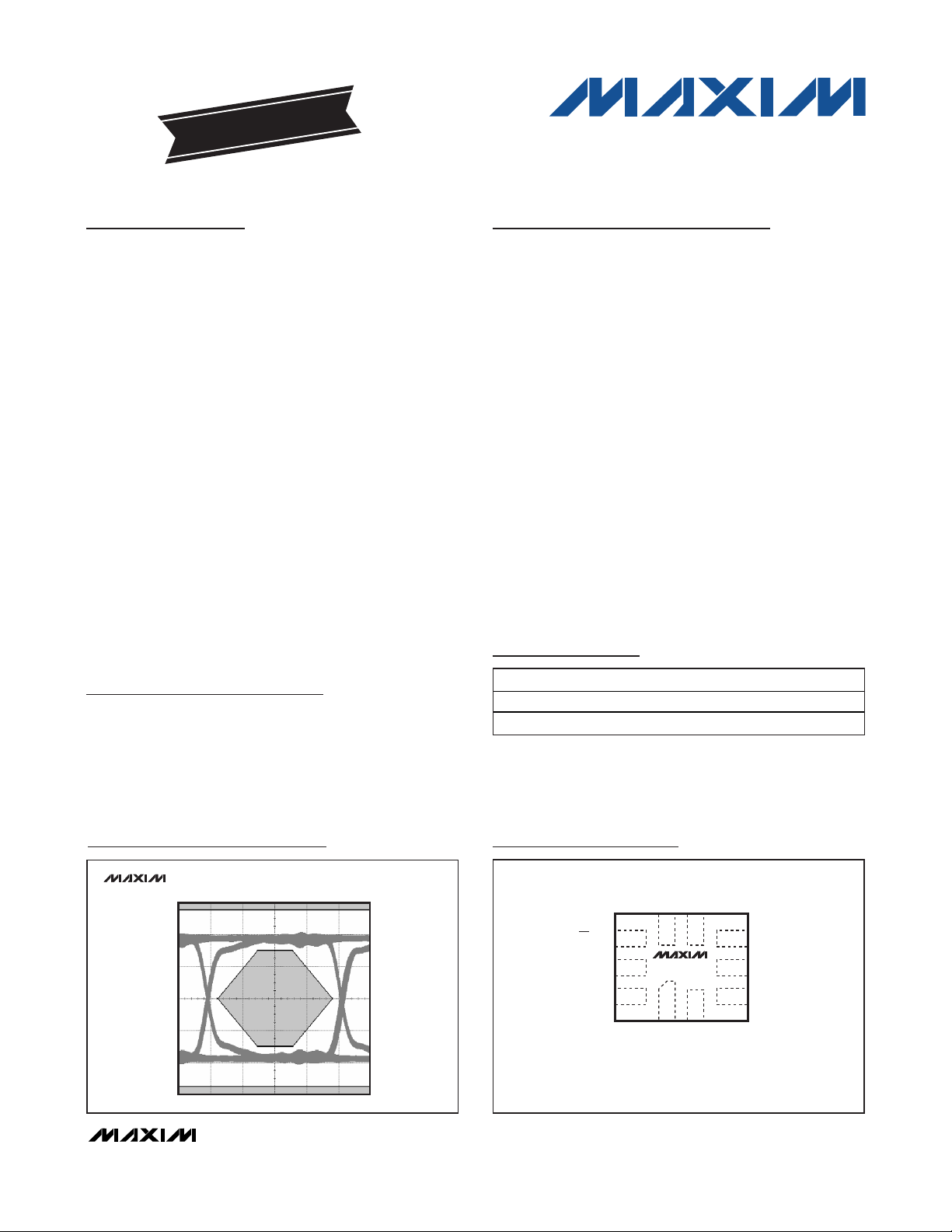
Eye Diagram
Note: All devices operate over the -40°C to +85°C extended
temperature range.
+
Denotes a lead-free package.
Ordering Information
PART PIN-PACKAGE TOP MARK
MAX4983EEVB+ 10 Ultra-Thin QFN AAA
MAX4984EEVB+ 10 Ultra-Thin QFN AAB
NO2
NC2
7 6
8
MAX4983E/
9
MAX4984E
1 2
NC1
UTQFN
NO1
5
COM2
4
GND
3
COM1
MAX4983E
MAX4984E
TOP VIEW
EN (EN)
V
USB 2.0
Hi-SPEED
TRANSMIT
TEMPLATE
(EN) FOR MAX4984E ONLY.
CC
10
CB
Page 2
MAX4983E/MAX4984E
Hi-Speed USB 2.0 Switches
with ±15kV ESD
2 _______________________________________________________________________________________
ABSOLUTE MAXIMUM RATINGS
ELECTRICAL CHARACTERISTICS
(VCC= +2.8V to +5.5V, TA= -40°C to +85°C, unless otherwise noted. Typical values are at VCC= +3.0V, TA= +25°C.) (Note 2)
Stresses beyond those listed under “Absolute Maximum Ratings” may cause permanent damage to the device. These are stress ratings only, and functional
operation of the device at these or any other conditions beyond those indicated in the operational sections of the specifications is not implied. Exposure to
absolute maximum rating conditions for extended periods may affect device reliability.
(All voltages referenced to GND.)
V
CC
, COM_, NO_, NC_, EN, EN, CB.................... -0.3V to +6.0V
Continuous Current into Any Terminal............................. ±30mA
Continuous Power Dissipation (T
A
= +70°C)
10-Pin UTQFN (derate 6.9mW/°C above +70°C)........ 559mW
Junction-to-Case Thermal Resistance (
θ
JC
) (Note 1)
10-Pin UTQFN ...........................................................20.1°C/W
Junction-to-Ambient Thermal Resistance (
θ
JA
) (Note 1)
10-Pin UTQFN ........................................................ 143.1°C/W
Operating Temperature Range .......................... -40°C to +85°C
Junction Temperature Range ......................................... +150°C
Storage Temperature Range ............................ -65°C to +150°C
Lead Temperature (soldering 10s) ..................................+300°C
)
)
Note 1: Package thermal resistances were obtained using the method described in JEDEC specification JESD51-7, using a four-
layer board. For detailed information on package thermal considerations, refer to www.maxim-ic.com/thermal-tutorial
.
PARAMETER SYMBOL CONDITIONS MIN TYP MAX UNITS
O p er ati ng P ow er - S up p l y Rang eV
Supply Current I
Shutdown Supply Current I
Increase in Supply Current
with V
, VEN Voltage
CB
Analog Signal Range
Fault-Protection Trip Threshold V
On-Resistance R
On-Resistance Match Between
Channels
On-Resistance Flatness R
Off-Leakage Current I
On-Leakage Current I
CC
SHDN
V
COM
V
ΔR
FLAT
COM(OFF
COM(ON
CC
, VNO,
NC
FP
ON
ON
VCB = 0V or VCC,
V
= 0V or VEN = V
EN
VCC = 3.0V 0.6 1.5
CC
VCC = 5.5V 3 6.5
Switch disabled (VEN = VCC or VEN = 0V) 0.1 µA
≤ VIL or VIH ≤ VCB ≤ VCC or 0 ≤ V
0 ≤ V
CB
≤ VIL or VIH ≤ VEN ≤ V
V
= VCC or VEN = 0V (Note 3) 0 V
EN
CC
EN
COM_ only, TA = +25°C
V
= 0V to V
COM
V
= 3.6V, VCC = 3.0V 5.5
COM
VCC = 3.0V, V
VCC = 3.0V, V
VCC = 4.5V, V
, VNC = 4.5V or 0V
V
NO
VCC = 5.5V, V
, VNC with 50µA sink current to GND
V
NO
VCC = 5.5V, V
, VNC = unconnected
V
NO
CC
= 2V (Note 4) 0.1 1 Ω
COM
= 0V to VCC (Note 5) 0.1 Ω
COM
= 0V or 4.5V,
COM
= 0V or 5.5V,
COM
= 0V or 5.5V,
COM
AC PERFORMANCE
On-Channel -3dB Bandwidth BW RL = RS = 50Ω, signal = 0dBm 950 MHz
f = 10MHz -48
f = 250MHz -20Off-Isolation V
f = 500MHz -17
ISO
VNO, VNC = 0dBm,
= RS = 50Ω
R
L
(Figure 1)
2.8 5.5 V
V
+
CC
0.6
-250 +250 nA
-250 +250 nA
2µA
CC
VCC +
0.8
V
+
C C
1
510
180 µA
µA
V
V
Ω
dB
Page 3
MAX4983E/MAX4984E
Hi-Speed USB 2.0 Switches
with ±15kV ESD
_______________________________________________________________________________________ 3
ELECTRICAL CHARACTERISTICS (continued)
(VCC= +2.8V to +5.5V, TA= -40°C to +85°C, unless otherwise noted. Typical values are at VCC= +3.0V, TA= +25°C.) (Note 2)
)
)
)
)
Note 2: All devices are 100% production tested at TA= +25°C. All temperature limits are guaranteed by design.
Note 3: The switch turns off for voltages above V
FP
, protecting downstream circuits in case of a fault condition.
Note 4: ΔR
ON(MAX)
= ABS(R
ON(CH1)
- R
ON(CH2)
).
Note 5: Flatness is defined as the difference between the maximum and minimum value of on-resistance, as measured over specified
analog signal ranges.
Note 6: Between any two switches.
Note 7: Switch off-capacitance, switch on-capacitance, and output skew between switches are not production tested; guaranteed by
design.
PARAMETER SYMBOL CONDITIONS MIN TYP MAX UNITS
VNO, VNC = 0dBm,
= RS = 50Ω,
CT
R
L
Figure 1
LOGIC INPUT
Input Logic-High V
Input Logic-Low V
Input Leakage Current I
IH
IL
IN
DYNAMIC
V
or V
Turn-On Time t
Turn-Off Time t
Propagation Delay t
PLH
Fault Protection Response
Time
Fault Protection Recovery
Time
Output Skew Between
Switches
C
NO_ or NC_ Off-Capacitance
COM Off-Capacitance
(Figure 5, Note 7)
COM On-Capacitance
(Figure 5, Note 7)
Total Harmonic Distortion Plus
Noise
NO(OFF
C
C
COM(OFF
C
COM(ON
THD+N
ON
OFF
, t
PHLRL
t
FP
t
FPR
t
SK
NC(OFF
N O
V
EN
V
N O
V
E N
= RS = 50Ω, Figure 3 100 ps
V
COM
V
CC
V
COM
V
CC
S kew b etw een sw i tch 1 and 2, RL = RS = 50Ω ,
( Fi g ur e 3, N ote 7)
or
f = 1MHz (Figure 5, Note 7) 2 pF
f = 1MHz 5.5
f = 240MHz 4.8
f = 1MHz 6.5
f = 240MHz 5.5
V
COM
f = 20Hz to 20kHz
= 1.5V , RL = 300Ω , C L = 35p F,
N C
= V
to 0V or V
C C
or V
= 1.5V , RL = 300Ω , C L = 35p F,
N C
= V
to 0V or V EN = 0V to V
C C
= 0V to 5V step, RL = RS = 50Ω,
= 3.3V (Figure 4)
= 5V to 0V step, RL = RS = 50Ω,
= 3.3V (Figure 4)
= 1V
P-P
, V
BIAS
ESD PROTECTION
Human Body Model ±15
IEC 61000-4-2 Air-Gap Discharge ±15COM1, COM2
IEC 61000-4-2 Contact Discharge ±8
All Pins Human Body Model ±2
f = 10MHz -73
f = 250MHz -54Crosstalk (Note 6) V
f = 500MHz -33
= 0V to V
E N
( Fi g ur e 2)
C C
( Fi g ur e 2)
C C
= 1V, RL = RS = 50Ω,
1.4 V
0.5 V
-250 +250 nA
20 100 µs
15µs
0.5 5.0 µs
100 µs
40 ps
0.03 %
dB
pF
pF
kV
Page 4
MAX4983E/MAX4984E
Hi-Speed USB 2.0 Switches
with ±15kV ESD
4 _______________________________________________________________________________________
Test Circuits/Timing Diagrams
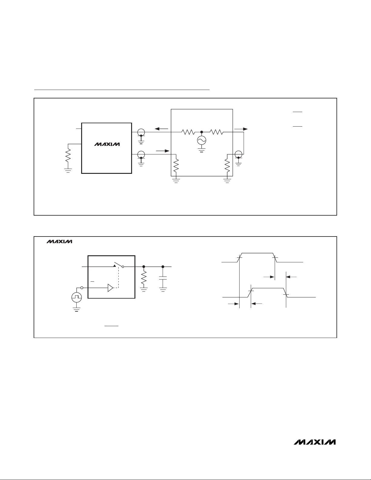
Figure 1. Off-Isolation and Crosstalk
Figure 2. Switching Time
NETWORK
ANALYZER
0V OR V
50Ω
V
CB
CC
NC1
MAX4983E/
MAX4984E
COM1
NO1*
IN
V
OUT
50Ω
MEAS REF
50Ω 50Ω
V
OUT
V
IN
V
OUT
V
IN
50Ω
OFF-ISOLATION = 20log
CROSSTALK = 20log
SWITCH IS ENABLED.
MEASUREMENTS ARE STANDARDIZED AGAINST SHORTS AT IC TERMINALS.
OFF-ISOLATION IS MEASURED BETWEEN COM_ AND "OFF" NO_ OR NC_ TERMINAL ON EACH SWITCH.
CROSSTALK IS MEASURED FROM ONE CHANNEL TO THE OTHER CHANNEL.
SIGNAL DIRECTION THROUGH SWITCH IS REVERSED; WORST VALUES ARE RECORDED.
MAX4983E/
MAX4984E
COM
R
L
L
)
ON
LOGIC
INPUT
NO
V
IN_
OR NC
EN (EN)
CL INCLUDES FIXTURE AND STRAY CAPACITANCE.
V
RL + R
OUT
= V
IN_ (
R
*FOR CROSSTALK THIS PIN IS NO2.
NC2 AND COM2 ARE OPEN.
V
IH
LOGIC
INPUT
V
V
OUT
C
L
SWITCH
OUTPUT
IL
0V
50%
V
OUT
0.9 x V
0UT
t
ON
IN DEPENDS ON SWITCH CONFIGURATION;
INPUT POLARITY DETERMINED BY SENSE OF SWITCH.
tR < 5ns
tF < 5ns
t
OFF
0.1 x V
OUT
Page 5

MAX4983E/MAX4984E
Hi-Speed USB 2.0 Switches
with ±15kV ESD
_______________________________________________________________________________________ 5
Test Circuits/Timing Diagrams (continued)
Figure 3. Output Signal Skew, Rise/Fall Time, Propagation Delay
MAX4983E/
50%
MAX4984E
CB
t
PHLX
VIL TO V
COM1
COM2
IH
50%
50%
50%
V
OUT+
t
= t
PLH
PLHX
t
= t
PHL
R
L
V
OUT-
R
L
t
INRISE
10% 10%
t
PHLX
t
= |t
SK(O)
= |t
t
SK(P)
90%
OUTRISE
90%
10% 10%
PLHX
PLHX
OR t
OR t
- t
- t
PLHY
PHLY
PLHY
PHLX
90%
| OR |t
| OR |t
90%
PHLX
PLHY
t
INFALL
- t
PHLY
- t
PHLY
t
OUTFALL
|
|
NC1 OR
R
S
R
S
PLHX
NO1
NC2 OR
NO2
50%
50%
V
IN+
V
IN-
V
CC
V
IN+
0V
V
CC
V
IN-
0V
t
V
CC
V
OUT+
0V
V
CC
V
OUT-
0V
t
PHLY
50%
t
PLHY
50%
Page 6

MAX4983E/MAX4984E
Hi-Speed USB 2.0 Switches
with ±15kV ESD
6 _______________________________________________________________________________________
Figure 4. Fault-Protection Response/Recovery Time
Test Circuits/Timing Diagrams (continued)
Figure 5. Channel Off-/On-Capacitance
MAX4983E/
MAX4984E
VCC = 3.3V
V
COM
t
FP
V
V
NO
V
NC
FP
CAPACITANCE
METER
COM
NC_ OR
NO_
t
FPR
MAX4983E/
MAX4984E
CB
5V
3V
0V
3V
0V
OR V
V
IL
IH
Page 7

MAX4983E/MAX4984E
Hi-Speed USB 2.0 Switches
with ±15kV ESD
_______________________________________________________________________________________ 7
Typical Operating Characteristics
(VCC= 3.0V, TA= +25°C, unless otherwise noted.)
ON-RESISTANCE vs. V
6
5
4
(Ω)
3
ON
R
2
1
0
0231456
VCC = 2.8V
VCC = 5.5V
V
COM
COM
MAX4983E/4E toc01
(V)
QUIESCENT SUPPLY CURRENT
vs. TEMPERATURE
4.0
3.5
3.0
2.5
2.0
1.5
1.0
QUIESCENT SUPPLY CURRENT (μA)
0.5
0
-40 -15 10 35 60 85
VCC = 5.5V
VCC = 2.8V
TEMPERATURE (°C)
MAX4983E/4E toc04
FREQUENCY RESPONSE
0
-10
-20
-30
-40
-50
-60
MAGNITUDE (dB)
-70
-80
-90
-100
1 1,00010010
ON-LOSS
OFF-ISOLATION
FREQUENCY (MHz)
ON-RESISTANCE vs. V
7
6
5
4
(Ω)
ON
R
3
2
1
0
0
12
V
COM
QUIESCENT SUPPLY CURRENT
vs. LOGIC LEVEL
5
4
3
2
1
QUIESCENT SUPPLY CURRENT (μA)
0
0123
LOGIC LEVEL (V)
MAX4983E/4E toc07
CROSSTALK
COM
TA = -40°CTA = +85°C TA = +25°C
(V)
TOTAL HARMONIC DISTORTION
PLUS NOISE vs. FREQUENCY
1
RL = 600Ω
0.1
THD+N (%)
0.01
0.001
10 100 1,000
3
80
70
MAX4983E/4E toc02
60
50
40
30
LEAKAGE CURRENT (nA)
20
10
0
1.2
1.0
MAX4983E/4E toc05
0.8
0.6
0.4
LOGIC THRESHOLD (V)
0.2
0
FREQUENCY (Hz)
COM LEAKAGE CURRENT
vs. TEMPERATURE
COM ON-LEAKAGE
COM OFF-LEAKAGE
-40 -15 10 35 60 85
TEMPERATURE (°C)
LOGIC-INPUT THRESHOLD
vs. SUPPLY VOLTAGE
V
V
IL
IH
2.8 3.8 4.8
SUPPLY VOLTAGE (V)
MAX4983E/4E toc08
10,000 100,000
MAX4983E/4E toc03
MAX4983E/4E toc06
Page 8

MAX4983E/MAX4984E
Detailed Description
The MAX4983E/MAX4984E are ±15kV ESD-protected
DPDT analog switches. The devices are ideal for USB
2.0 Hi-Speed (480Mbps) switching applications and
also meet USB low- and full-speed requirements.
The MAX4983E/MAX4984E are fully specified to operate from a single +2.8V to +5.5V supply. The low V
IH
threshold of the devices permits them to be used with
logic levels as low as 1.4V. The MAX4983E/MAX4984E
are based on a charge-pump-assisted n-channel architecture. The devices feature a shutdown mode to
reduce the quiescent current to less than 0.1µA (typ).
Digital Control Input
The MAX4983E/MAX4984E provide a single-bit control
logic input, CB. CB controls the position of the switches
as shown in the
Functional Diagram/Truth Table
.
Driving CB rail-to-rail minimizes power consumption.
With a +2.8V to +5.5V supply voltage range, the device
is +1.4V logic compatible.
Analog Signal Levels
The on-resistance of the MAX4983E/MAX4984E is very
low and stable as the analog input signals are swept
from ground to VCC(see the
Typical Operating Character-
istics
). These switches are bidirectional, allowing NO_,
NC_, and COM_ to be configured as either inputs or
outputs. The charge-pump-assisted n-channel architecture allows the switch to pass analog signals that
exceed V
CC
up to the overvoltage fault protection
threshold. This allows USB signals that exceed VCCto
pass, allowing compliance with USB requirements for
voltage levels.
Overvoltage Fault Protection
The MAX4983E/MAX4984E feature overvoltage fault protection on COM_. Fault protection protects the switch and
USB transceiver from damaging voltage levels. When
voltages on COM exceed the fault protection threshold,
(VFP), COM_, NC_ and NO_ are high impedance.
Enable Input
The MAX4983E/MAX4984E feature a shutdown mode that
reduces the supply current to less than 0.1µA and places
COM_ in high impedance. Drive EN high for the
MAX4983E or EN low for the MAX4984E to place the
devices in shutdown mode. When EN is driven low or EN
is driven high, the devices are in normal operation.
Applications Information
USB Switching
The MAX4983E/MAX4984E analog switches are fully compliant with the USB 2.0 specification. The low on-resistance and low on-capacitance of these switches make
them ideal for high-performance switching applications.
Hi-Speed USB 2.0 Switches
with ±15kV ESD
8 _______________________________________________________________________________________
Pin Description
PIN
MAX4983E MAX4984E
1 1 NC1 Normally Closed Terminal for Switch 1
2 2 NO1 Normally Open Terminal for Switch 1
3 3 COM1 Common Terminal for Switch 1
4 4 GND Ground
5 5 COM2 Common Terminal for Switch 2
6 6 NO2 Normally Open Terminal for Switch 2
7 7 NC2 Normally Closed Terminal for Switch 2
8—EN
—8EN
99V
10 10 CB
NAME FUNCTION
Active-Low Enable Input. Drive EN high to put switches in high impedance. Drive EN
low for normal operation.
Active-High Enable Input. Drive EN low to put switches in high impedance. Drive EN
high for normal operation.
CC
Positive Supply Voltage Input. Bypass VCC to GND with a 0.1µF ceramic capacitor as
close as possible to the device.
Digital Control Input. Drive CB low to connect COM_ to NC_. Drive CB high to connect
COM_ to NO_.
Page 9

The MAX4983E/MAX4984E are ideal for routing USB
data lines (see Figure 6) and for applications that
require switching between multiple USB hosts (see
Figure 7). The MAX4983E/MAX4984E also feature
overvoltage fault protection to guard systems against
shorts to the USB VBUS voltage that is required for all
USB applications.
Extended ESD Protection
As with all Maxim devices, ESD-protection structures
are incorporated on all pins to protect against electrostatic discharges encountered during handling and
assembly. COM1 and COM2 are further protected
against static electricity. The ESD structures withstand
high ESD in normal operation and when the device is
powered down. After an ESD event, the MAX4983E/
MAX4984E continue to function without latchup.
The MAX4983E and MAX4984E are characterized for
protection to the following limits:
• ±15kV using Human Body Model
• ±8kV using IEC 61000-4-2 Contact Discharge method
• ±15kV using IEC 61000-4-2 Air-Gap Discharge method
ESD Test Conditions
ESD performance depends on a variety of conditions.
Contact Maxim for a reliability report that documents
test setup, test methodology, and test results.
Human Body Model
Figure 8a shows the Human Body Model and Figure 8b
shows the current waveform it generates when discharged into a low impedance. This model consists of a
100pF capacitor charged to the ESD voltage of interest,
which is then discharged into the test device through a
1.5kΩ resistor.
IEC 61000-4-2
The main difference between tests done using the Human
Body Model and IEC 61000-4-2 is higher peak current in
IEC 61000-4-2. Because series resistance is lower in the
IEC 61000-4-2 ESD test model (Figure 9a), the ESD-withstand voltage measured to this standard is generally
lower than that measured using the Human Body Model.
Figure 9b shows the current waveform for the ±8kV
IEC 61000-4-2 Level 4 ESD Contact Discharge test.
The Air-Gap Discharge test involves approaching the
device with a charged probe. The Contact Discharge
method connects the probe to the device before the
probe is energized.
Layout
USB Hi-Speed requires careful PCB layout with 45Ω
controlled-impedance matched traces of equal lengths.
Ensure that bypass capacitors are as close as possible
to the device. Use large ground planes where possible.
Power-Supply Sequencing
Caution: Do not exceed the absolute maximum ratings because stresses beyond the listed ratings
may cause permanent damage to the device.
Proper power-supply sequencing is recommended for all
devices. Always apply V
CC
before applying analog sig-
nals, especially if the analog signal is not current limited.
Chip Information
PROCESS: BiCMOS
MAX4983E/MAX4984E
Hi-Speed USB 2.0 Switches
with ±15kV ESD
_______________________________________________________________________________________ 9
Functional Diagram/Truth Table
CB
NO1
NC1
NO2
NC2
V
CC
CB
EN
0
0
1
X = DON'T CARE.
EN
CB
1
1
0
X = DON'T CARE.
MAX4983E
0
1
X
MAX4984E
0
1
X
GND
N0_
OFF
ON
OFF
N0_
OFF
ON
OFF
EN (EN)
MAX4983E/
MAX4984E
NC_
ON
OFF
OFF
NC_
ON
OFF
OFF
COM1
COM2
COM_
—
—
HI-Z
COM_
—
—
HI-Z
Page 10

MAX4983E/MAX4984E
Hi-Speed USB 2.0 Switches
with ±15kV ESD
10 ______________________________________________________________________________________
Figure 6. USB Data Routing/Typical Application Circuit
Figure 8b. Human Body Current Waveform
Figure 8a. Human Body ESD Test Model
Figure 7. Switching Between Multiple USB Hosts
Figure 9b. IEC 61000-4-2 ESD Generator Current Waveform
Figure 9a. IEC 61000-4-2 ESD Test Model
ASIC I
HI-SPEED
USB
TRANSCEIVER
ASIC II
HI-SPEED
USB
TRANSCEIVER
D+
MAX4983E/
D-
D+
D-
NC1
NO1
NC2
NO2
MAX4984E
COM1
COM2
V
BUS
D+
D-
GND
USB
CONNECTOR
TRANSCEIVER
HI-SPEED
USB
MAX4983E/
MAX4984E
NC1
COM1
D+
D-
COM2
NO1
NC2
NO2
D+
USB
HOST I
D-
D+
USB
HOST II
D-
R
D
1500Ω
DISCHARGE
RESISTANCE
STORAGE
CAPACITOR
DEVICE
UNDER
TEST
HIGH-
VOLTAGE
DC
SOURCE
R
C
1MΩ
CHARGE-CURRENT-
LIMIT RESISTOR
C
s
100pF
R
D
330Ω
DISCHARGE
RESISTANCE
STORAGE
CAPACITOR
DEVICE
UNDER
TEST
HIGH-
VOLTAGE
DC
SOURCE
R
C
50MΩ to 100MΩ
CHARGE-CURRENT-
LIMIT RESISTOR
C
s
150pF
PEAK-TO-PEAK RINGING
I
R
(NOT DRAWN TO SCALE)
AMPERES
IP 100%
90%
36.8%
10%
0
0
t
RL
TIME
t
DL
CURRENT WAVEFORM
I
100%
90%
PEAK
I
10%
t
= 0.7ns to 1ns
R
30ns
60ns
t
Page 11

MAX4983E/MAX4984E
Hi-Speed USB 2.0 Switches
with ±15kV ESD
______________________________________________________________________________________ 11
Package Information
For the latest package outline information, go to www.maxim-ic.com/packages.
PACKAGE TYPE PACKAGE CODE DOCUMENT NO.
10 Ultra-Thin QFN V101A1CN-1
21-0028
Page 12

MAX4983E/MAX4984E
Hi-Speed USB 2.0 Switches
with ±15kV ESD
Maxim cannot assume responsibility for use of any circuitry other than circuitry entirely embodied in a Maxim product. No circuit patent licenses are
implied. Maxim reserves the right to change the circuitry and specifications without notice at any time.
12
____________________Maxim Integrated Products, 120 San Gabriel Drive, Sunnyvale, CA 94086 408-737-7600
© 2008 Maxim Integrated Products is a registered trademark of Maxim Integrated Products, Inc.
Revision History
REVISION
NUMBER
0 2/08 Initial release —
1 5/08 Removal of future product asterisks, global change to Hi-Speed 1, 8, 9, 10
2 9/08 Changes to EC table 3
REVISION
DATE
DESCRIPTION
PAGES
CHANGED
 Loading...