

________________General Description
The MAX496 and MAX497 are quad, closed-loop, ±5V
video buffers that feature extremely high bandwidth and
slew rate for both component video (RGB or YUV) and
composite video (NTSC, PAL, SECAM). The MAX496 is
a unity-gain (0dB) buffer with a 375MHz -3dB bandwidth
and a 1600V/µs slew rate. The MAX497 gain of +2 (6dB)
buffer, optimized for driving back-terminated coaxial
cable, features a 275MHz -3dB bandwidth and a
1500V/µs slew rate. The MAX496/MAX497 are not slewrate limited, thus providing a high full-power bandwidth
of 230MHz and 215MHz, respectively.
The MAX496/MAX497 incorporate a unique two-stage
architecture that combines the low offset and noise
benefits of voltage feedback with the high bandwidth
and slew-rate advantages of current-mode-feedback.
________________________Applications
Computer Workstations
Surveillance Video
Broadcast and High-Definition TV Systems
Multimedia Products
Medical Imaging
High-Speed Signal Processing
Video Switching and Routing
____________________________Features
♦ MAX496 Fixed Gain: +1V/V
MAX497 Fixed Gain: +2V/V
♦ High Speed:
Small-Signal -3dB Bandwidth: 375MHz (MAX496)
275MHz (MAX497)
Full-Power -3dB Bandwidth: 230MHz (MAX496)
215MHz (MAX497)
♦ 0.1dB Gain Flatness: 65MHz (MAX496)
120MHz (MAX497)
♦ 1600V/µs Slew Rate (MAX496)
1500V/µs Slew Rate (MAX497)
♦ Fast Settling Time: 12ns to 0.1%
♦ Lowest Differential Phase/Gain Error: 0.01°/0.01%
♦ 2pF Input Capacitance
♦ 5.6nV/√Hz Input-Referred Voltage Noise
♦ Low Distortion: 64dBc (f = 10MHz)
♦ Directly Drives 50Ω or 75Ω Back-Terminated Cables
♦ High ESD Protection: 5000V
♦ Output Short-Circuit Protected
MAX496/MAX497
375MHz Quad Closed-Loop
Video Buffers, AV= +1 and +2
________________________________________________________________
Maxim Integrated Products
1
16
15
14
13
12
11
10
9
1
2
3
4
5
6
7
8
OUT0
V
CC
OUT1
V
EE
IN1
GND
IN0
GND
TOP VIEW
MAX496
MAX497
OUT2
V
EE
OUT3
V
CC
IN3
GND
IN2
GND
DIP/SO
___________________Pin Configuration
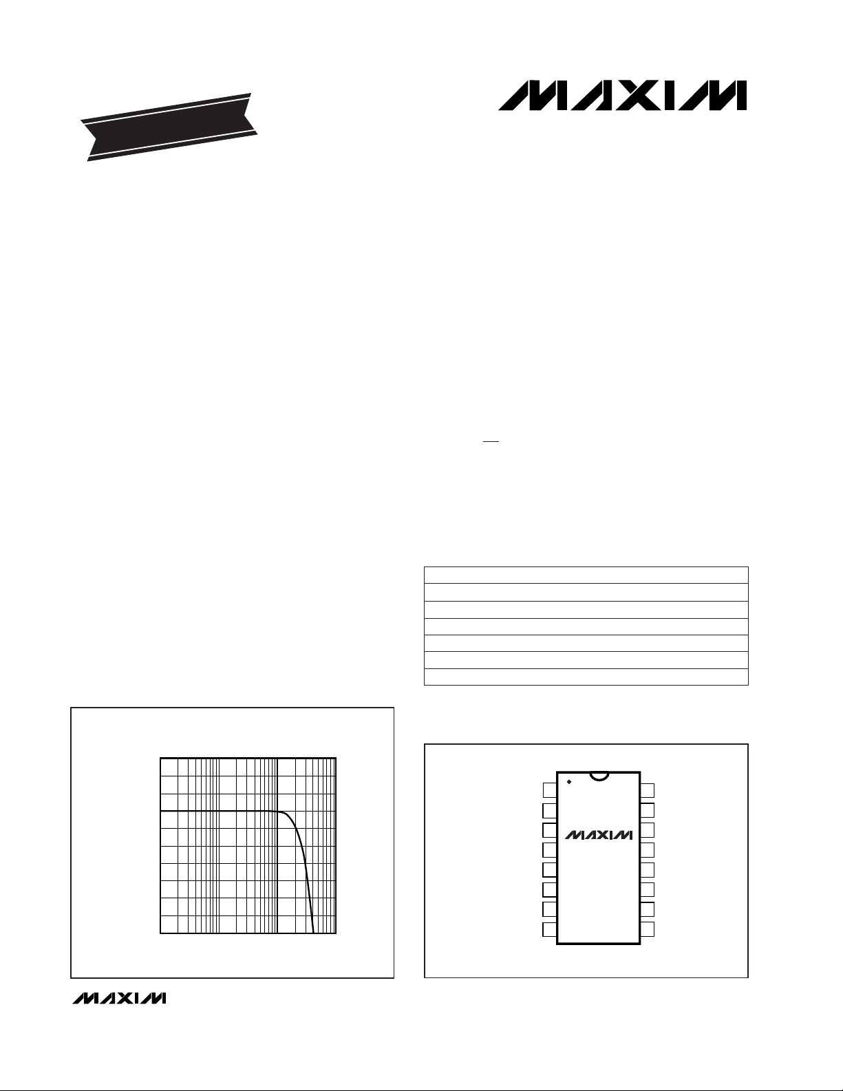
1M 10M 1G
MAX497
SMALL-SIGNAL GAIN vs. FREQUENCY
-1
0
1
2
3
4
5
6
7
8
9
MAX496/97-A
FREQUENCY (Hz)
GAIN (dB)
100M
_______________Frequency Response
19-0373; Rev 1; 12/98
PART
MAX496CPE
MAX496CSE
MAX496C/D 0°C to +70°C
0°C to +70°C
0°C to +70°C
TEMP. RANGE PIN-PACKAGE
16 Plastic DIP
16 Narrow SO
Dice*
EVALUATION KIT MANUAL
FOLLOWS DATA SHEET
_______________Ordering Information
* Dice are specified at TA = +25°C, DC parameters only.
MAX497CPE
0°C to +70°C 16 Plastic DIP
MAX497CSE 0°C to +70°C 16 Narrow SO
MAX497C/D 0°C to +70°C Dice*
For free samples & the latest literature: http://www.maxim-ic.com, or phone 1-800-998-8800.
For small orders, phone 1-800-835-8769.
MAX496/MAX497
375MHz Quad Closed-Loop
Video Buffers, AV= +1 and +2
2 _______________________________________________________________________________________
ABSOLUTE MAXIMUM RATINGS
DC ELECTRICAL CHARACTERISTICS
(VCC= +5V, VEE= -5V, VIN= 0V, RL= 150Ω, TA= T
MIN
to T
MAX
, unless otherwise noted. Typical values are at TA= +25°C.)
Stresses beyond those listed under “Absolute Maximum Ratings” may cause permanent damage to the device. These are stress ratings only, and functional
operation of the device at these or any other conditions beyond those indicated in the operational sections of the specifications is not implied. Exposure to
absolute maximum rating conditions for extended periods may affect device reliability.
Supply Voltage (VCCto VEE)................................................. 12V
Voltage on Any Input Pin to GND ....(V
CC
+ 0.3V) to (VEE- 0.3V)
Output Short-Circuit Current Duration ...............................60sec
Continuous Power Dissipation (T
A
= +70°C)
Plastic DIP (derate 10.53mW/°C above +70°C) ..........842mW
Narrow SO (derate 8.70mW/°C above +70°C) ............696mW
Operating Temperature Range...............................0°C to +70°C
Storage Temperature Range.............................-65°C to +150°C
Lead Temperature (soldering, 10sec).............................+300°C
R
L
= 50Ω
RL= 150Ω
V
OUT
= 0V
TA = T
MIN
to T
MAX
TA= +25°C
MAX497
TA = T
MIN
to T
MAX
MAX496
TA= +25°C
A
VCL
= +2, V
OUT
= ±1mV to ±2V
VEE= ±4.5V to ±5.5V, VCC= 5.0V
MAX496 (Note 1)
VCC= ±4.5V to ±5.5V, VEE= -5.0V
V
OUT
= 0V
V
OUT
= 0V
MAX496: -2V ≤ VIN≤ +2V,
MAX497: -1V ≤ VIN≤ +1V
MAX497 (Note 2)
CONDITIONS
V
±2.5 ±3.3
V
OUT
Output Voltage Swing
±2.8 ±3.7
V±4.50 ±5.50V
S
Operating Supply Voltage Range
mA
45
ISY-
Negative Quiescent Supply
Current (Total)
32 37
mA
45
ISY+
Positive Quiescent Supply
Current (Total)
31 36
%0.01A
VLIN
Gain Linearity
dB60 78PSRR-
Negative Power-Supply
Rejection Ratio (Change in VOS)
dB55 74PSRR+
Positive Power-Supply Rejection
Ratio (Change in VOS)
V/V
1.965 2.01
A
V
Voltage Gain
mV±1 ±3V
OS
Input Offset Voltage
V
±1.4 ±1.6
V
IN
±2.8 ±3.2
Input Voltage Range
1.975 2.01
0.983 1.00
0.988 1.00
pF2C
IN
Input Capacitance
µV/°C-10TCV
OS
Input Offset Voltage Drift
µA±1 ±5I
B
Input Bias Current
MΩ0.5 1.2R
IN
Input Resistance
UNITSMIN TYP MAXSYMBOLPARAMETER
Output Resistance R
OUT
DC 0.1 Ω
Output Impedance Z
OUT
f = 10MHz 1.5 Ω
Short-Circuit Output Current I
SC
Short to ground or either supply voltage 170 mA
RL= 150Ω
RL= 50Ω
RL= 150Ω
RL= 50Ω
Small-Signal -3dB Bandwidth
MAX496/MAX497
375MHz Quad Closed-Loop
Video Buffers, AV= +1 and +2
_______________________________________________________________________________________ 3
AC ELECTRICAL CHARACTERISTICS
(VCC= +5V, VEE= -5V, VIN= 0V, RL= 100Ω, TA= +25°C.)
Note 1: Voltage Gain = (V
OUT
- VOS) / VIN, measured at VIN= ±1V.
Note 2: Voltage Gain = (V
OUT
- VOS) / VIN, measured at VIN= ±2V.
Note 3: Input test signal is a 3.58MHz sine wave of amplitude 40 IRE superimposed on a linear ramp (0 IRE to 100 IRE).
R
L
= 150Ω, see Figure 2.
Note 4: Input of channel under test grounded through 75Ω. Adjacent channel driven at f = 10MHz (Figure 4a). For All-Hostile
Crosstalk, all inputs are driven except the channel under test (Figure 4b).
fC= 5MHz
V
OUT
= ±2V
MAX496CPE
fC= 10MHz,
V
OUT
= 2Vp-p
MAX496CSE
f = 10MHz
f = 10MHz
f = 3.58MHz (Note 3)
f = 3.58MHz (Note 3)
V
OUT
= 4V step, MAX496
V
OUT
= 4V step, MAX497
0.1% (VOUT = 2V step)
CONDITIONS
dBc
60
SFDR
58
Spurious-Free Dynamic Range
THDTotal Harmonic Distortion dBc
-58
-64
dB
72
78
MHz
80
80
230
375
375
pA√Hz2Input Noise Current Density
nV√Hz5.6Input Noise Voltage Density
degrees0.01DPDifferential Phase Error
%0.01DGDifferential Gain Error
MHz
215
FPBWFull-Power Bandwidth
1600
V/µs
1500
SRSlew Rate
ns12t
s
Settling Time
UNITSMIN TYP MAXSYMBOLPARAMETER
MAX496CPE
MAX496CSE
MAX496
MAX497
MAX496
MAX497
MAX496
MAX497
±0.1dB
120
Gain Flatness
MAX497CPE 100
MAX497CSE
(Note 4) dB
72
Adjacent Channel Crosstalk
MAX496
MAX497
65
All-Hostile Crosstalk (Note 4)
MAX496
MAX497
MAX497CPE
MAX497CSE
MHz
275
BW
-3dB
275
Small-Signal -3dB Bandwidth
MAX496/MAX497
375MHz Quad Closed-Loop
Video Buffers, AV= +1 and +2
4 _______________________________________________________________________________________
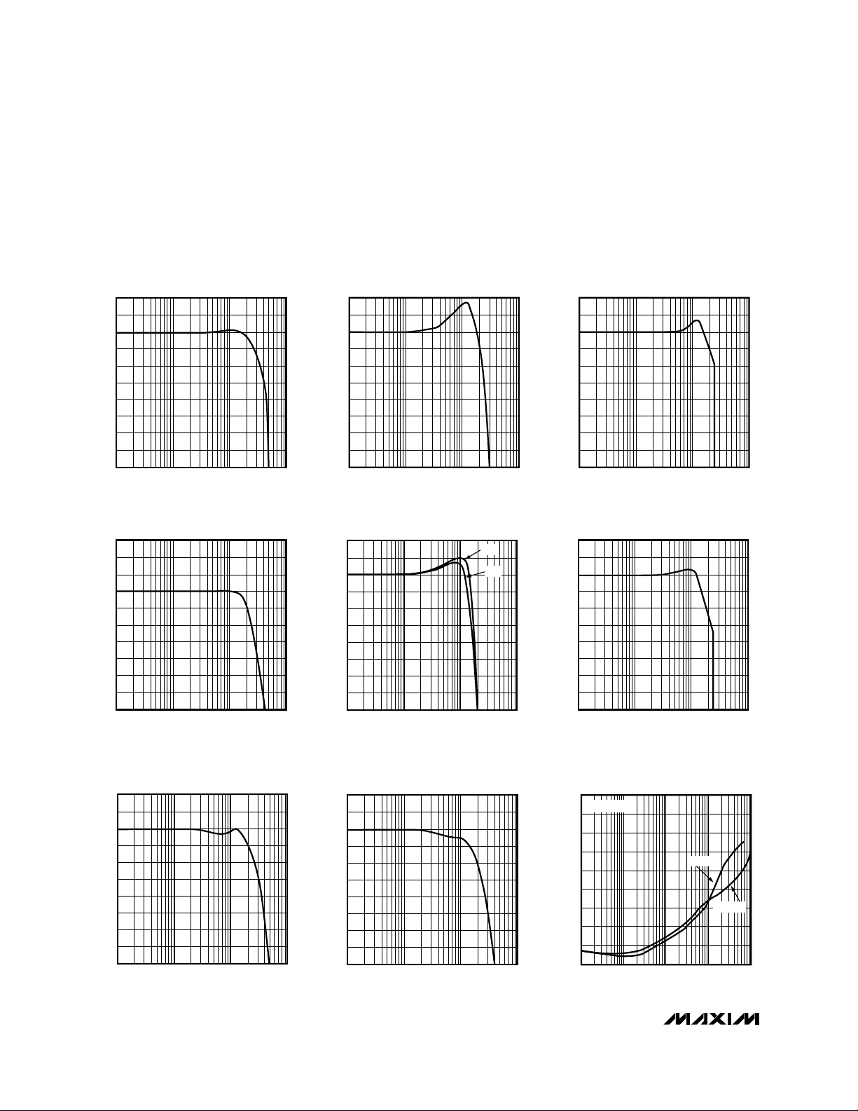
__________________________________________Typical Operating Characteristics
(VCC= +5V, VEE= -5V, RL= 100Ω, TA= +25°C, unless otherwise noted.)
1M 10M 1G
MAX496
SMALL-SIGNAL GAIN vs. FREQUENCY
-8
-7
-6
-5
-4
-3
-2
-1
0
1
2
MAX496/97-01
FREQUENCY (Hz)
GAIN (dB)
100M
MAX496
GAIN FLATNESS vs. FREQUENCY
-0.8
-0.7
-0.6
-0.5
-0.4
-0.3
-0.2
-0.1
0
0.1
0.2
MAX496/97-02
FREQUENCY (Hz)
GAIN (dB)
1M 10M 1G100M
MAX496
LARGE-SIGNAL GAIN vs. FREQUENCY
-8
-7
-6
-5
-4
-3
-2
-1
0
1
2
MAX496/97-03
FREQUENCY (Hz)
GAIN (dB)
1M 10M 1G100M
MAX497
SMALL-SIGNAL GAIN vs. FREQUENCY
-1
0
1
2
3
4
5
6
7
8
9
MAX496/97-04
FREQUENCY (Hz)
GAIN (dB)
1M 10M 1G100M
1M 10M 1G
MAX496
SMALL-SIGNAL GAIN vs. FREQUENCY
DRIVING A 50Ω LOAD
-8
-7
-6
-5
-4
-3
-2
-1
0
1
2
MAX496/97-07
FREQUENCY (Hz)
GAIN (dB)
100M
MAX497
GAIN FLATNESS vs. FREQUENCY
5.3
5.2
5.4
5.5
5.6
5.7
5.8
5.9
6.0
6.1
6.2
MAX496/97-05
FREQUENCY (Hz)
GAIN (dB)
1M 10M 1G100M
SO
DIP
MAX497
LARGE-SIGNAL GAIN vs. FREQUENCY
-1
-2
0
1
2
3
4
5
6
7
8
MAX496/97-06
FREQUENCY (Hz)
GAIN (dB)
1M 10M 1G100M
1M 10M 1G
MAX497
SMALL-SIGNAL GAIN vs. FREQUENCY
DRIVING A 50Ω LOAD
-2
-1
0
1
2
3
4
5
6
7
8
MAX496/97-08
FREQUENCY (Hz)
GAIN (dB)
100M
0
-90
10k 1M 10M100k 100M
TOTAL HARMONIC DISTORTION (THD)
vs. FREQUENCY
-80
-70
-60
-50
-40
-30
-20
-10
MAX496/97-09
FREQUENCY (Hz)
DISTORTION (dB)
MAX497
MAX496
V
OUT
= 2Vp-p

MAX496
GAIN MATCH vs. FREQUENCY
-0.6
-0.7
-0.5
-0.4
-0.3
-0.2
-0.1
0.0
0.1
0.2
0.3
MAX496/97-13a
FREQUENCY (Hz)
GAIN MATCH (dB)
1M 10M 1G100M
CH 2–CH 1
CH 3–CH 0
CH 3–CH 1
CH 3–CH 2
CH 1–CH 0
CH 2–CH 0
MAX496/MAX497
375MHz Quad Closed-Loop
Video Buffers, AV= +1 and +2
_______________________________________________________________________________________
5
-10
-110
1 10 200100
MAX496
CROSSTALK vs. FREQUENCY
-90
MAX496/97-10
FREQUENCY (MHz)
CROSSTALK (dB)
-70
-50
-30
-100
-80
-60
-40
-20
ALL-HOSTILE
ADJACENT CHANNEL
-10
0
1M 1G
MAX497
CROSSTALK vs. FREQUENCY
-70
-90
-100
-30
-20
-40
-60
-80
-50
MAX496/97-11
FREQUENCY (Hz)
CROSSTALK (dB)
10M
100M
ADJACENT CHANNEL
ALL-HOSTILE
-90
-100
20k 1M 10M100k 100M
POWER-SUPPLY REJECTION (PSR)
vs. FREQUENCY
-80
-70
-60
-50
-40
-30
-20
-10
MAX496/97-12
FREQUENCY (Hz)
POWER-SUPPLY REJECTION (dB)
MAX497
MAX496
MAX497
GAIN MATCH vs. FREQUENCY
-0.4
-0.5
-0.3
-0.2
-0.1
0
0.1
0.2
0.3
0.4
0.5
MAX496/97-13b
FREQUENCY (Hz)
GAIN MATCH (dB)
1M 10M 1G100M
CH 2–CH 0
CH 1–CH 0
CH 3–CH 1
CH 3–CH 0
CH 3–CH 2
CH 2–CH 1
-0.30
-0.20
-0.10
0
0.10
0.20
0.30
-40 -20 0 20 40 60 80 100
INPUT OFFSET VOLTAGE
vs. TEMPERATURE
MAX496/97-16
TEMPERATURE (°C)
OFFSET VOLTAGE (mV)
1.000
0.990
-40 -20 0 20 40 60 80 100
MAX496
GAIN vs. TEMPERATURE
0.992
0.998
MAX496/97-14
TEMPERATURE (°C)
GAIN (V/V)
0.996
0.994
0.991
0.993
0.999
0.997
0.995
VIN = -1.0V
VIN = -1.0V
2.05
1.95
-40 -20 0 20 40 60 80 100
MAX497
GAIN vs. TEMPERATURE
1.97
2.03
MAX496/97-15
TEMPERATURE (°C)
GAIN (V/V)
2.01
1.99
1.96
1.98
2.04
2.02
2.00
V
IN
= +1.0V
V
IN
= -1.0V
38
40
-10 0 10 80
SUPPLY CURRENT
vs. TEMPERATURE
26
22
20
34
36
32
28
24
30
MAX496/97-17
TEMPERATURE (°C)
SUPPLY CURRENT (mA)
20 30 40 50 60 70
I
EE
RL = NO LOAD
I
CC
_____________________________Typical Operating Characteristics (continued)
(VCC= +5V, VEE= -5V, RL= 100Ω, TA= +25°C, unless otherwise noted.)

MAX496/MAX497
375MHz Quad Closed-Loop
Video Buffers, AV= +1 and +2
6 _______________________________________________________________________________________
_____________________________Typical Operating Characteristics (continued)
(VCC= +5V, VEE= -5V, RL= 100Ω, TA= +25°C, unless otherwise noted.)
0.05
VOLTAGE (V)
IN
OUT
-0.05
0.05
-0.05
MAX496
SMALL-SIGNAL PULSE RESPONSE
MAX496/97-18
TIME (10ns/div)
1.0
-1.0
IN
OUT
-1.0
1.0
MAX496
LARGE-SIGNAL PULSE RESPONSE
MAX496/97-20
TIME (10ns/div)
VOLTAGE (V)
IN
-0.50
to 0.50
OUT
-0.10
to 0.10
MAX497
SMALL-SIGNAL PULSE RESPONSE
MAX496/97-19
TIME (10ns/div)
VOLTAGE (V)
IN
1.0
-1.0
VOLTAGE (V)
OUT
2.0
-2.0
MAX497
LARGE-SIGNAL PULSE RESPONSE
MAX496/97-21
TIME (10ns/div)

MAX496/MAX497
375MHz Quad Closed-Loop
Video Buffers, AV= +1 and +2
_______________________________________________________________________________________
7
-0.05
IN
0.05
0.05
OUT
VOLTAGE (V)
-0.05
MAX496
SMALL-SIGNAL PULSE RESPONSE
(C
L
= 47pF
MAX496/97-22
10ns/div
IN
0.50
-0.50
OUT
0.10
-0.10
MAX497
SMALL-SIGNAL PULSE RESPONSE
(C
L
= 47pF)
MAX496/97-23
10ns/div
VOLTAGE (V)
1.0
IN
-1.0
1.0
OUT
-1.0
MAX496
LARGE-SIGNAL PULSE RESPONSE
(C
L
= 47pF)
MAX496/97-24
10ns/div
VOLTAGE (V)
1.0
-1.0
IN
2.0
-2.0
OUT
MAX497
LARGE-SIGNAL PULSE RESPONSE
(C
L
= 47pF)
MAX496/97-25
10ns/div
VOLTAGE (V)
_____________________________Typical Operating Characteristics (continued)
(VCC= +5V, VEE= -5V, RL= 100Ω, TA= +25°C, unless otherwise noted.)

MAX496/MAX497
_______________Detailed Description
The MAX496/MAX497 are quad, high-speed, closed-loop
voltage-feedback video amplifiers with fixed gain settings
of +1 and +2, respectively (Figure 1). These amplifiers
use a unique two-stage voltage-feedback architecture
that combines the benefits of conventional voltage-feedback and current-mode-feedback topologies. They
achieve wide bandwidths and high slew rates while maintaining precision. A resistively loaded first stage provides
low input-referred noise even with low supply currents of
8mA per amplifier. The above features, along with the
ability to drive 50Ω or 75Ω back-terminated cables to
±2.8V and low differential phase and gain errors, make
these amplifiers ideal for the most demanding component
and composite video applications.
__________Applications Information
The feedback elements of the MAX496/MAX497 are
included internally in the device to set the closed-loop
gain to AV= +1 and AV= +2, respectively. Closing the
loop internally on the chip minimizes problems associated with the board and package parasitics influencing
the amplifier’s frequency response.
375MHz Quad Closed-Loop
Video Buffers, AV= +1 and +2
8 _______________________________________________________________________________________
_____________________Pin Description
Channel 2 OutputOUT212
Channel 3 InputIN38
Positive Power Supply. Connect to +5V.
V
CC
pins are internally connected.
Connect both pins to +5V externally to
minimize the supply impedance.
V
CC
9, 15
Channel 3 OutputOUT310
Negative power supply. Connect to -5V.
V
EE
pins are internally connected.
Connect both pins to -5V externally to
minimize the supply impedance.
V
EE
11, 13
Channel 2 InputIN26
Channel 0 InputIN02
PIN
Ground. All ground pins are internally
connected. Connect all ground pins
externally to minimize the ground
impedance.
GND
1, 3,
5, 7
FUNCTIONNAME
14 OUT1 Channel 1 Output
16 OUT0 Channel 0 Output
Figure 1. Typical Operating Circuit
MAX496*
MAX497*
OUT0
2
RED
GREEN
BLUE
SYNC
159
GND
4
6
8
16
IN0
0.10µF
0.10µF
10µF 10µF
0.10µF
+5V
-5V
V
CC
V
EE
*AV = +1 (MAX496)
*A
V
= +2 (MAX497)
A
V
= *
A
V
= *
IN1
IN2
IN3
753
75Ω
75Ω CABLE
75Ω CABLE
75Ω CABLE
75Ω CABLE
75Ω CABLE
75Ω CABLE
75Ω CABLE
75Ω CABLE
75Ω
75Ω
75Ω
AV = *
OUT1
14
75Ω
75Ω
75Ω
75Ω
OUT2
12
75Ω
75Ω
75Ω
75Ω
OUT3 10
75Ω
75Ω
75Ω
75Ω
1311
0.10µF
Channel 1 InputIN14

Power Dissipation
The maximum output current of the MAX496/MAX497 is
limited by the packages maximum allowable power dissipation. The maximum junction temperature should not
exceed +150°C. The power dissipation increases with
load, and this increase can be approximated by the following:
For V
OUT
> 0V: |V
CC
- V
OUT|ILOAD
OR
For V
OUT
< 0V: |V
EE
- V
OUT|ILOAD
.
These devices can drive 100Ω loads connected to
each of the outputs over the entire rated output swing
and temperature range. When driving 50Ω loads with
each of the four outputs simultaneously, the output
swing must be limited to ±1.25V at TA= +70°C. While
the output is short-circuit protected to 170mA, this does
not necessarily guarantee that, under all conditions, the
maximum junction temperature will not be exceeded.
Do not exceed the derating values given in the
absolute maximum ratings.
MAX496/MAX497
375MHz Quad Closed-Loop
Video Buffers, AV= +1 and +2
_______________________________________________________________________________________ 9
75Ω CABLE
75Ω CABLE
75Ω CABLE
75Ω
75Ω
75Ω
75Ω
75Ω CABLE
75Ω
75Ω
150Ω
SOURCE:
TEKTRONIX
1910 DIGITAL GENERATOR
MEASUREMENT:
TEKTRONIX VM700
VIDEO MEASUREMENT
SET
MAX497
MAX496
DUT
DUT
a)
b)
Figure 2. Differential Phase and Gain Error Test Circuits: a) MAX497, Gain of +2 Amplifier; b) MAX496 Unity-Gain Amplifier
MAX496/MAX497
75Ω
OUT1
OUT2
OUT3
OUT4
75Ω
IN0
75Ω
75Ω
75Ω
75Ω
75Ω
75Ω
75Ω
Figure 3. One-to-Four Distribution Amplifier

MAX496/MAX497
Total Noise
The MAX496/MAX497’s low input current noise of
2pA/√Hz and voltage noise of 5.6nV/√Hz provide for
lower total noise compared to typical current-modefeedback amplifiers, which usually have significantly
higher input current noise. The input current noise multiplied by the feedback resistor is the dominant noise
source of current-mode-feedback amplifiers.
Differential Gain and Phase Errors
Differential gain and phase errors are critical specifications for a buffer in composite (NTSC, PAL, SECAM) video
applications, because these errors correspond directly to
color changes in the displayed picture of composite video
systems. The MAX496/MAX497’s ultra-low differential gain
and phase errors (0.01%/ 0.01°) make them ideal in
broadcast-quality composite video applications.
Distribution Amplifier
The circuit in Figure 3 is a one-to-four distribution amplifier
using a single MAX496 or MAX497 IC. A one-to-eight distribution amplifier can be implemented with a MAX496 or
MAX497 by driving an additional cable from each of the
four outputs. When driving more than four outputs from a
single device, see the Continuous Power Dissipation
specifications in the
Absolute Maximum Ratings
.
Coaxial Cable Drivers
High-speed performance, excellent output current
capability, and an internally fixed gain of +2 make the
MAX497 ideal for driving back-terminated 50Ω or 75Ω
coaxial cables to ±2.8V.
In a typical application, the MAX497 drives a back-terminated 75Ω video cable (Figure 1). The back-termination resistor (at the MAX497’s output) matches the
impedance of the cable’s driven end to the cable’s
impedance, to eliminate signal reflections. This, along
with the load-termination resistor, forms a voltage
divider with the load impedance, which attenuates the
signal at the cable output by one-half. The MAX497
operates with an internal +2V/V closed-loop gain to provide unity gain at the cable’s output.
Capacitive Load Driving
In most amplifier circuits, driving large capacitive loads
increases the likelihood of oscillation. This is especially
true for circuits with high loop gains, such as voltage
followers. The amplifier’s output resistance and the
capacitive load form an RC filter that adds a pole to the
loop response. If the pole frequency is low enough (as
when driving a large capacitive load), the circuit phase
margin is degraded and oscillation may occur.
375MHz Quad Closed-Loop
Video Buffers, AV= +1 and +2
10 ______________________________________________________________________________________
MAX496/MAX497
MAX496/MAX497
VIN = 4Vp-p,
f = 10MHz,
R
S
= 75Ω
100Ω
100Ω
100Ω
100Ω
50Ω
50Ω
50Ω
50Ω
VIN = 4Vp-p,
f = 10MHz,
R
S
= 75Ω
100Ω
100Ω
100Ω
100Ω
50Ω
50Ω
50Ω
50Ω
a) ADJACENT CHANNEL b) ALL-HOSTILE
Figure 4. Crosstalk: a) Adjacent Channel; b) All-Hostile

The MAX496/MAX497 drive capacitive loads up to 75pF
without sustained oscillation, although some peaking
may occur. When driving larger capacitive loads, or to
reduce peaking, add an isolation resistor (R
ISO
) between
the output and the capacitive load (Figures 5a–5d).
Grounding and Layout
The MAX496/MAX497 bandwidths are in the RF frequency range. Depending on the size of the PC board
used and the frequency of operation, it may be necessary to use Micro-strip or Stripline techniques.
To realize the full AC performance of these high-speed
buffers, pay careful attention to power-supply bypassing
and board layout. The PC board should have at least two
layers (wire-wrap boards are too inductive, bread boards
are too capacitive), with one side a signal layer and the
other a large, low-impedance ground plane. With multilayer boards, locate the ground plane on the layer that is not
dedicated to a specific signal trace. The ground plane
should be as free from voids as possible. Connect all
ground pins to the ground plane.
Connect both positive power-supply pins together and
bypass with a 0.10µF ceramic capacitor at each power
supply pin, as close to the device as possible. Repeat
the same for the negative power-supply pins. The
capacitor lead lengths should be as short as possible
to minimize lead inductance; surface-mount chip
capacitors are ideal. A large-value (4.7µF or greater)
tantalum or electrolytic bypass capacitor on each supply may be required for high-current loads. The location
of this capacitor is not critical.
The MAX496/MAX497’s analog input pins are isolated
with ground pins to minimize parasitic coupling, which can
degrade crosstalk and/or amplifier stability. Keep signal
paths as short as possible to minimize inductance. Ensure
that all input channel traces are the same length to maintain the phase relationship between the four channels. To
further reduce crosstalk, connect the coaxial-cable shield
to the ground side of the 75Ω terminating resistor at the
ground plane, and terminate all unused inputs ground and
outputs with a 100Ω or 150Ω resistor to ground.
MAX496/MAX497
375MHz Quad Closed-Loop
Video Buffers, AV= +1 and +2
______________________________________________________________________________________ 11
1M 10M 1G
-12
-10
-8
-6
-4
-2
0
2
4
6
8
MAX496/97-5a
FREQUENCY (Hz)
GAIN (dB)
100M
CL = 22pF
CL = 10pF
CL = 0pF
CL = 47pF
CL = 60pF
RL = 50Ω
R
ISO
= 0Ω
Figure 5a. MAX496 Small-Signal Gain vs. Frequency and Load
Capacitor (R
L
= 50Ω, R
ISO
= 0Ω)
1M 10M 1G
-30
-25
-20
-15
-10
-5
0
5
10
15
20
MAX496/97-5c
FREQUENCY (Hz)
GAIN (dB)
100M
CL = 10pF
CL = 0pF
CL = 47pF
CL = 68pF
RL =
R
ISO
= 0Ω
8
CL = 20pF
Figure 5c. MAX496 Small-Signal Gain vs. Frequency and Load
Capacitor (R
L
= ∞, R
ISO
= 0Ω)
1M 10M 1G
-5
-4
-3
-2
-1
0
1
2
3
4
5
MAX496/97-5b
FREQUENCY (Hz)
* -3dB ATTENUATION DUE
TO R
ISO
NOT SHOWN
GAIN (dB)*
100M
CL = 22pF
CL = 47pF
RL = 50Ω
R
ISO
= 20Ω
CL = 60pF
CL = 10pF
Figure 5b. MAX496 Small-Signal Gain vs. Frequency and
Load Capacitor (R
L
= 50Ω, R
ISO
= 20Ω)
Figure 5d. MAX496 Small-Signal Gain vs. Frequency and
Load Capacitor (R
L
= ∞, R
ISO
= 20Ω)
20
15
RL =
R
10
5
0
-5
GAIN (dB)
-10
-15
-20
-25
-30
1M 10M 1G
ISO
= 20Ω
8
CL = 68pF
FREQUENCY (Hz)
CL = 22pF
CL = 10pF
100M
CL = 47pF
MAX496/97-5d

MAX496/MAX497
375MHz Quad Closed-Loop
Video Buffers, AV= +1 and +2
12 ______________________________________________________________________________________
________________________________________________________Package Information
___________________Chip Topography
TRANSISTOR COUNT: 544
SUBSTRATE CONNECTED TO V
EE
OUT1
IN2
IN3
0.101"
(2.56mm)
GND
V
CC
OUT3
V
EE
OUT2
V
EE
IN0
GND
OUT0 V
CC
GND
IN1
GND
0.076"
(1.930mm)
SOICN.EPS
 Loading...