

Page 1
现货库存、技术资料、百科信息、热点资讯,精彩尽在鼎好!
General Description
The MAX4947/MAX4948 analog switches operate from a
single +1.8V to +5.5V supply. These switches feature a
low 30pF (typ) capacitance for high-speed data switching applications.
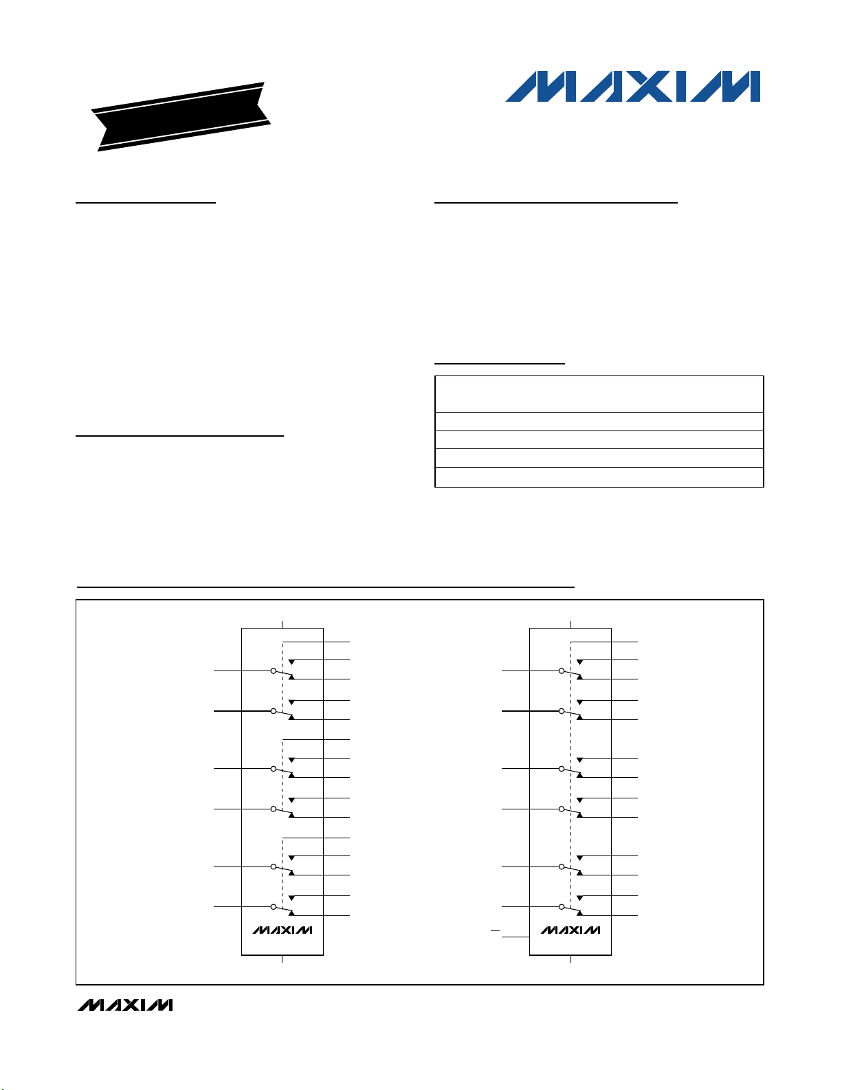
The MAX4947 is a triple double-pole/double-throw (DPDT)
switch, and the MAX4748 is a hex single-pole/doublethrow (SPDT) switch with one control logic input. The
MAX4947 has three logic inputs to control the switches in
pairs. The MAX4948 has one logic input and an enable
input (EN) to disable the switches.
The MAX4947/MAX4948 are available in small 24-pin
(4mm x 4mm) TQFN and 25-bump (2.5mm x 2.5mm)
chip-scale packages (UCSP™).
Applications
Features
♦ Multiplex SDIO or Memory Stick Interfaces
♦ 1.8V to 5.5V Supply Voltage Range
♦ Low On-Resistance 4Ω (typ)
♦ Low-Capacitance Switches, 30pF (typ)
♦ Rail-to-Rail Signal Handling
♦ Small 25-Bump UCSP™ (2.5mm x 2.5mm) and
24-TQFN (4mm x 4mm)
MAX4947/MAX4948
Hex SPDT Data Switch
________________________________________________________________
Maxim Integrated Products
1
Ordering Information
MAX4947
S6
S5
COM6
COM5
S4
S3
COM4
COM3
S2
S1
V
CC
COM2
COM1
GND
NO1
NC1
NO2
NC2
NO3
NC3
NO4
NC4
NO5
NC5
NO6
NC6
CB12
CB34
CB56
MAX4948
S6
S5
COM6
COM5
S4
S3
COM4
COM3
S2
S1
V
CC
COM2
COM1
GND
NO1
NC1
NO2
NC2
NO3
NC3
NO4
NC4
NO5
NC5
NO6
NC6
CB
EN
Functional Diagram
19-0673; Rev 1; 1/07
For pricing, delivery, and ordering information, please contact Maxim/Dallas Direct! at
1-888-629-4642, or visit Maxim’s website at www.maxim-ic.com.
*
Future product—contact factory for availability.
+
Denotes lead-free package.
EP = Exposed paddle.
EVALUATION KIT
AVAILABLE
USB Signal Switching
UART Signal Switching
SDIO/Memory Stick
Cell Phones
PDAs
Typical Operating Circuit appears at end of data sheet.
UCSP is a trademark of Maxim Integrated Products, Inc.
PART
TEMP
RANGE
MAX4947EBA+* -40°C to +85°C 25 UCSP-25 B25-1
MAX4947ETG+ -40°C to +85°C 24 TQFN-EP T2444-4
MAX4948EBA+* -40°C to +85°C 25 UCSP-25 B25-1
MAX4948ETG+ -40°C to +85°C 24 TQFN-EP T2444-4
PINPACKAGE
PKG
CODE
Page 2
MAX4947/MAX4948
Hex SPDT Data Switch
2 _______________________________________________________________________________________
ABSOLUTE MAXIMUM RATINGS
ELECTRICAL CHARACTERISTICS
(VCC= +2.7V to +5.5V, TA= -40°C to +85°C, unless otherwise noted. Typical values are at VCC= +3V, TA= +25°C.) (Notes 2, 3)
Stresses beyond those listed under “Absolute Maximum Ratings” may cause permanent damage to the device. These are stress ratings only, and functional
operation of the device at these or any other conditions beyond those indicated in the operational sections of the specifications is not implied. Exposure to
absolute maximum rating conditions for extended periods may affect device reliability.
VCCto GND ...........................................................-0.3V to +6.0V
All other pins to GND (Note 1)......................-0.3V to V
CC
+ 0.3V
Continuous Current
NO_, NC_, COM_ .......................................................±100mA
Peak Current NO_, NC_, COM_
(pulsed at 1ms, 50% Duty Cycle)................................±200mA
(pulsed at 1ms, 10% Duty Cycle)................................±300mA
Continuous Power Dissipation (T
A
= +70°C)
25-Bump UCSP (derate 12.2mW/°C above +70°C) ....976mW
24-Pin TQFN (derate 20.8mW/°C above +70°C) .......1667mW
Operating Temperature Range ...........................-40°C to +85°C
Junction Temperature ........................................................150°C
Storage Temperature Range .............................-65°C to +150°C
Bump Temperature (soldering)
Infrared (15s) ...............................................................+220°C
Vapor Phase (60s) ...........................................................+215°C
Lead Temperature (soldering) .........................................+300°C
(
)
(ON)
Note 1: Signals on CB_, NO_, NC_, COM_, EN exceeding VCCor GND are clamped by internal diodes. Limit forward-diode current
to maximum current rating.
PARAMETER SYMBOL CONDITIONS T
POWER SUPPLY
Power-Supply Range V
CC
VCC = 5.5V, VCB_ = 0V or V
CC
VCC = 2.7V, VCB_ = 1.6V or 0.5V 5Power-Supply Current I
VCC = 5.5V, VCB_ = 1.6V or 0.5V
ANALOG SWITCH
MIN TYP MAX UNITS
A
T
to
CC
T
T
T
MIN
MAX
MIN
MAX
1.8 5.5 V
1.0
to
10
µA
Analog Signal Range
_, VNC_,
NO
V
COM
_,
T
T
MIN
MAX
to
0V
V
+25°C 4.0 5.5
On-Resistance (Note 4) R
ON
VCC = 2.7V, I
_ or VNO_ = 0 or V
V
NC
COM
_ = 10mA;
CC
T
T
MIN
MAX
to
+25°C 0.3 0.5
On-Resistance Match Between
Channels (Notes 4, 5)
ΔR
ON
VCC = 2.7V, I
V
_ or VNC_ = 0 or V
NO
COM
_ = 10mA;
CC
T
T
MIN
MAX
to
+25°C 0.5 1
On-Resistance Flatness
(Notes 4, 6)
R
FLAT
VCC = 2.7V, I
COM
_ = 10mA;
VNC_ or VNO_ = 0 or V
CC
T
T
MIN
MAX
to
+25°C -3 +3
NO_ or NC_ Off-Leakage
Current
COM_ On-Leakage Current INO_
INO_
I
NC
(OFF)
_
OFF
or
VCC = 3.6V; V
V
NO
VCC = 3.6V; V
V
NO
unconnected
_ = 3.6V, 0;
COM
_ or VNC_ = 0, 3.6V
_ = 3.6V, 0;
COM
_ or VNC_ = 3.6V, 0 or
T
to
T
MIN
MAX
-10 +10
+25°C -6 +6
to
T
T
MIN
MAX
-10 +10
CC
6.5
0.6
1.2
V
Ω
Ω
Ω
nA
nA
Page 3
MAX4947/MAX4948
Hex SPDT Data Switch
_______________________________________________________________________________________ 3
(
)
(
)
(ON)
ELECTRICAL CHARACTERISTICS (continued)
(VCC= +2.7V to +5.5V, TA= -40°C to +85°C, unless otherwise noted. Typical values are at VCC= +3V, TA= +25°C.) (Notes 2, 3)
PARAMETER SYMBOL CONDITIONS T
VCC = 3.6V (MAX4948);
COM_ Off-Leakage Current I
COM
_
OFF
V
_ = 3.3V, 0.3V;
COM
_ or VNC_ = 0, 3V, 3.3V
V
NO
DYNAMIC
VCC = 2.7V; VNO_ or VNC_= 1.5V;
Turn-On Time t
ON
= 50Ω;
R
L
C
= 35pF, Figure 1
L
VCC = 2.7V; VNO_ or VNC_= 1.5V;
Turn-Off Time t
Break-Before-Make t
OFF
BBM
= 50Ω;
R
L
C
= 35pF, Figure 1
L
V
= 2.7V; VNO_ or VNC_= 1.5V;
CC
R
= 50Ω; CL = 35pF, Figure 2
L
(Note 7)
HIGH-SPEED TIMING CHARACTERISTICS (rising time = 20ns)
Skew t
SKEW
Charge Injection Q
-3dB Bandwidth BW
VCC = 2.7V; RS = 39Ω; CL = 50pF,
Figure 3
V
= 0, R
GEN
GEN
Figure 4
Signal = 0dBm, C
= 50Ω, Figure 5
R
L
CL = 5pF; RL = 50Ω;
Off-Isolation V
ISO
V
COM
_ = 1V
P-P
Figure 5 (Note 8)
Crosstalk V
C
NC_ or NO_ Off-Capacitance
COM_ Off-Capacitance C
COM_ On-Capacitance C
NC_(OFF)
CNO_
C OM _ ( OF F)
COM
CT
CL = 5pF; RL = 50Ω; f = 1MHz,
_ = 1V
V
COM
P-P
NC_ = NO_ = 0V, f = 1MHz
Figure 6
OFF
V
= GND, f = 1MHz
COM
(MAX4948), Figure 6
_
COM_ = 0V, f = 1MHz, Figure 6 +25°C 30 pF
DIGITAL I/O (EN, CB_)
Input-Logic High V
Input-Logic Low V
Input Leakage Current I
CB
IH
IL
V
= 0 or V
CB_
CC
= 0, CL = 1nF ,
= 5pF,
L
, f = 1MHz,
, Figure 5 (Note 9)
+25°C -6 +6
T
MIN
T
MAX
+25°C 400 800
T
MIN
T
MAX
+25°C 300 800
T
MIN
T
MAX
+25°C 100
T
MIN
T
MAX
T
MIN
T
MAX
+25°C 10 pC
+25°C 300 MHz
+25°C -70 dB
+25°C -90 dB
+25°C 15 pF
+25°C 25 pF
T
MIN
T
MAX
T
MIN
T
MAX
T
MIN
T
MAX
MIN TYP MAX UNITS
A
to
-10 +10
to
to
to
2
to
to
1.6 V
0.2 ns
to
to
800
800
0.5 V
1µA
nA
ns
ns
ns
Page 4
MAX4947/MAX4948
Hex SPDT Data Switch
4 _______________________________________________________________________________________
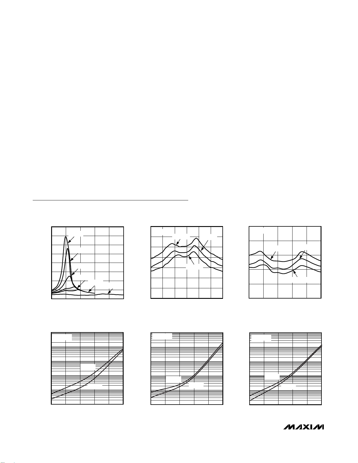
Typical Operating Characteristics
(VCC= 3V, TA = +25°C, unless otherwise noted.)
ON-RESISTANCE vs. V
COM
V
COM
(V)
ON-RESISTANCE (Ω)
MAX4947/48 toc01
012345
0
5
10
15
20
25
30
35
40
VCC = 1.8V
VCC = 2.0V
VCC = 2.3V
VCC = 2.7V
VCC = 3.0V
VCC = 5.0V
ON-RESISTANCE
vs. V
COM
TEMPERATURE
V
COM
(V)
R
ON
(Ω)
MAX4947/48 toc02
0 0.5 1.0 1.5 2.0 2.5 3.0
0
1
2
3
4
5
6
7
TA = +85°C
TA = +25°C
TA = -40°C
VCC = 3V
ON-RESISTANCE
vs. V
COM
AND TEMPERATURE
V
COM
(V)
R
ON
(Ω)
MAX4947/48 toc03
012345
0
1
2
3
4
5
TA = +85°C
TA = +25°C
TA = -40°C
VCC = 5V
NO/NC OFF-LEAKAGE CURRENT
vs. TEMPERATURE
MAX4947/48 toc04
TEMPERATURE (°C)
NO/NC OFF-LEAKAGE CURRENT (nA)
603510-15
0.001
0.01
0.1
1
10
0.0001
-40 85
VCC = 3V
VCC = 3V/5V
V
CC
= 5V
COM ON-LEAKAGE CURRENT
vs. TEMPERATURE
MAX4947/48 toc05
TEMPERATURE (°C)
COM ON-LEAKAGE CURRENT (nA)
603510-15
0.001
0.01
0.1
1
10
0.0001
-40 85
VCC = 3V
VCC = 3V/5V
VCC = 5V
COM OFF-LEAKAGE CURRENT
vs. TEMPERATURE (MAX4748)
MAX4947/48 toc06
TEMPERATURE (°C)
COM OFF-LEAKAGE CURRENT (nA)
603510-15
0.001
0.01
0.1
1
10
0.0001
-40 85
VCC = 3V
VCC = 3V/5V
VCC = 5V
Note 2: The algebraic convention is used. The most negative value is shown in the minimum column.
Note 3: UCSP parts are 100% tested at T
A
= +25°C. Limits across the full temperature range are guaranteed by correlation and
design. TQFN parts are guaranteed by correlation and design at - 40°C.
Note 4: R
ON
and ΔR
ON
matching specifications are guaranteed by design.
Note 5: ΔR
ON
= R
ON(MAX)
- R
ON(MIN)
.
Note 6: Flatness is defined as the difference between the maximum and minimum value of on-resistance as measured over the
specified analog signal ranges.
Note 7: Guaranteed by design, not production tested.
Note 8: Off-Isolation = 20log
10[VCOM_
/ (V
NO_
or V
NC_
)], V
COM_
= output, V
NO_
or V
NC_
= input to off switch.
Note 9: Between any two switches.
ELECTRICAL CHARACTERISTICS (continued)
(VCC= +2.7V to +5.5V, TA= -40°C to +85°C, unless otherwise noted. Typical values are at VCC= +3V, TA= +25°C.) (Notes 2, 3)
Page 5

MAX4947/MAX4948
Hex SPDT Data Switch
_______________________________________________________________________________________
5
Operating Characteristics (continued)
(VCC= +3V, TA = +25°C, unless otherwise noted.)
CHARGE INJECTION vs. V
25
CL = 1nF
20
V
V+ = 5V
COM
(V)
15
10
CHARGE INJECTION (pC)
5
0
V+ = 3V
012345
COM
MAX4947/48 toc07
LOGIC THRESHOLD vs. SUPPLY VOLTAGE
2.0
1.6
1.2
V
IH
0.8
LOGIC THRESHOLD (V)
0.4
0
1.5 2.5 3.5 4.5 5.5
SUPPLY VOLTAGE (V)
V
MAX4947/48 toc10
IL
FREQUENCY RESPONSE
20
0
-20
-40
-60
ON-LOSS (dB)
-80
-100
-120
-140
0.0001
ON-LOSS
MAX4947/48 toc13
OFF-ISOLATION
CROSSTALK
1000.01 1
FREQUENCY (MHz)
SUPPLY CURRENT vs. SUPPLY VOLTAGE
15
14
13
12
11
10
9
8
7
6
5
SUPPLY CURRENT (nA)
4
3
2
1
0
123456
SUPPLY VOLTAGE (V)
TURN-ON/-OFF TIME
1000
900
800
700
600
(ns)
500
OFF
/t
ON
400
t
300
200
100
0
1.5 2.5 3.5 4.5 5.5
1
0.1
THD+N (%)
0.01
0.01 0.1 1 10 100
vs. SUPPLY VOLTAGE
t
OFF
t
ON
SUPPLY VOLTAGE (V)
TOTAL HARMONIC DISTORTION
PLUS NOISE vs. FREQUENCY
R
= 600Ω
L
FREQUENCY (kHz)
100
MAX4947/48 toc08
10
1
SUPPLY CURRENT (nA)
0.1
-40 -15 10 35 60 85
TURN-ON/-OFF TIMES vs. TEMPERATURE
450
400
350
MAX4947/48 toc11
300
250
(ns)
OFF
/t
200
ON
t
150
100
50
0
-40 -15 10 35 60 85
7
6
MAX4947/48 toc14
5
4
3
2
SUPPLY CURRENT (μA)
1
0
SUPPLY CURRENT vs. TEMPERATURE
VCC = 5V
VCC = 3V
TEMPERATURE (°C)
tON, V+ = 3V
t
, V+ = 3V
OFF
t
OFF
, V+ = 5V
TEMPERATURE (°C)
tON, V+ = 5V
SUPPLY CURRENT vs. LOGIC VOLTAGE
VCC = 5.5V
1.6
01.00.5
2.0 3.0 4.0 5.0 6.0
LOGIC VOLTAGE (V)
MAX4947/48 toc09
MAX4947/48 toc12
MAX4947/48 toc15
Page 6

MAX4947/MAX4948
Hex SPDT Data Switch
6 _______________________________________________________________________________________6 _______________________________________________________________________________________
Pin Description
PIN NAME FUNCTION
MAX4947 MAX4948
TQFN UCSP TQFN UCSP
1 D2 1 D2 NC6 Analog Switch 6. Normally Closed Terminal 6.
2 D1 2 D1 NO5 Analog Switch 5. Normally Open Terminal 5.
3 C1 3 C1 COM5 Analog Switch 5. Common Terminal 5.
4 C2 4 C2 NC5 Analog Switch 5. Normally Closed Terminal 5.
5 B1 — — CB56 Digital Control Input for Analog Switches 5 and 6
6, 21
7 B2 7 B2 COM4 Analog Switch 4. Common Terminal 4.
8 A2 8 A2 NO4 Analog Switch 4. Normally Open Terminal 4.
9 B3 9 B3 NC4 Analog Switch 4. Normally Closed Terminal 4.
10 A3 10 A3 NO3 Analog Switch 3. Normally Open Terminal 3.
11 A4 11 A4 COM3 Analog Switch 3. Common Terminal 3.
12 B4 12 B4 NC3 Analog Switch 3. Normally Closed Terminal 3.
13 A5 — — CB34 Digital Control Input for Analog Switches 3 and 4
14 B5 — — CB12 Digital Control Input for Analog Switches 1 and 2
15 C4 15 C4 NC2 Analog Switch 2. Normally Closed Terminal 2.
16 C5 16 C5 COM2 Analog Switch 2. Common Terminal 2.
17 D5 17 D5 NO2 Analog Switch 2. Normally Open Terminal 2.
18 D4 18 D4 NC1 Analog Switch 1. Normally Closed Terminal 1.
19 E5 19 E5 NO1 Analog Switch 1. Normally Open Terminal 1.
20 E4 20 E4 COM1 Analog Switch 1. Common Terminal 2.
22 E3 22 E3 V
23 E2 23 E2 COM6 Analog Switch 6. Common Terminal 6.
24 E1 24 E1 NO6 Analog Switch 6. Normally Open Terminal 6.
—— 5 B1EN
— — 13 A5 N.C. No Connection. Leave N.C. unconnected.
— — 14 B5 CB
EP — EP — EP Exposed Pad. Connect exposed pad to ground.
A1, C3,
D3
6, 21
A1, C3,
D3
GND Ground
CC
Positive Supply Voltage
Enable-Logic In. Drive EN high to set all switches into highimpedance mode.
Digital Control Input for Analog Switches 1–6. Drive CB low to
connect COM_ to NC_ for all six switches. Drive CB high to connect
COM_ to NO_ for all six switches. CB is valid only when EN is driven
low. If EN is driven high then all switches are high impedance.
Page 7

MAX4947/MAX4948
Hex SPDT Data Switch
_______________________________________________________________________________________ 7
Pin Configurations/Truth Tables
(BUMPS SIDE DOWN) MAX4947
+
GND NO4 NO3
A
CB56 COM4 NC4
B
COM5 NC5 GND
C
NO5 NC6 GND
D
NO6 COM6 V
E
2345
1
CC
UCSP 2.5mm x 2.5mm
(BUMPS SIDE DOWN) MAX4948
1
2345
+
GND NO4 NO3
A
EN COM4 NC4
B
COM5 NC5 GND
C
NO5 NC6 GND
D
NO6 COM6 V
E
CC
UCSP 2.5mm x 2.5mm
COM3
NC3
NC2
NC1 NO2
COM1
COM3
NC3
NC2
NC1 NO2
COM1
CB34
CB12
COM2
NO1
N.C.
CB
COM2
NO1
TOP VIEW
TOP VIEW
NO2
NC1
1718 16 14 13
NO1
19
COM1
20
GND
21
22
V
CC
COM6
23
+
24
NO6
12
NO5
NC6
TQFN 4mm x 4mm
*EXPOSED PADDLE CONNECT TO GROUND
NO2
NC1
1718 16 14 13
NO1
19
COM1
20
GND
21
22
V
CC
COM6
23
+
24
NO6
12
NO5
NC6
TQFN 4mm x 4mm
COM2
15
MAX4947
456
3
COM5
COM2
15
MAX4948
3
456
COM5
NC2
NC5
NC2
NC5
CB12
CB56
CB
EN
*EP
*EP
CB34
GND
N.C.
GND
12
NC3
COM3
11
NO3
10
9
NC4
NO4
8
COM4
7
12
NC3
COM3
11
NO3
10
9
NC4
NO4
8
COM4
7
*EXPOSED PADDLE-CONNECT TO GROUND
MAX4947
CB12 NO1/NO2
0OFFON
NO3/NO4 NC3/NC4CB34
NO5/NO6 NC5/NC6CB56
NC1/INC2
ON
OFF ON0
ON OFF1
OFF ON0
ON OFF1
OFF1
EN CB
LOW LOW OFF
MAX4948
NO_
HIGH
ONLOW
XOFF
NC_
ON
OFF
OFFHIGH
Page 8

MAX4947/MAX4948
Hex SPDT Data Switch
8 _______________________________________________________________________________________
Timing Circuits/Timing Diagrams
tr < 5ns
tf < 5ns
50%
0V
LOGIC
INPUT
R
L
COM_
GND
CB_
C
L
INCLUDES FIXTURE AND STRAY CAPACITANCE.
V
OUT
= V
N_ (
R
L
)
RL + R
ON
V
N_
V
CC
t
OFF
0V
NO_
OR NC_
0.9 x V
0UT
0.9 x V
OUT
t
ON
V
OUT
SWITCH
OUTPUT
LOGIC
INPUT
IN DEPENDS ON SWITCH CONFIGURATION;
INPUT POLARITY DETERMINED BY SENSE OF SWITCH.
V
CC
C
L
V
CC
V
OUT
MAX4947/
MAX4948
50%
Figure 1. Switching Time
Detailed Description
The MAX4947 triple DPDT and the MAX4948 hex SPDT
analog switches operate from a single +1.8V to
+5.5V supply. These devices are fully specified for +3V
applications.
The MAX4947/MAX4948 have a guaranteed 4Ω (typ) onresistance and a low 30pF (typ) capacitance that makes
the switch ideal for data switching applications. The
MAX4947 has three logic inputs to control two switches in
pairs and the MAX4948 has one logic control input and
an enable input (EN) to disable the switches.
Applications Information
Digital Control Inputs
The MAX4947/MAX4948 provide a digital control logic
input, CB_. CB_ controls the position of the switches as
shown in the
Pin Configurations/Truth Tables
. Driving
CB_ rail-to-rail minimizes power consumption.
The MAX4948 features an EN input to turn all switches
on or off. When EN is driven high, CB is disabled, and
the analog inputs enter a high-impedance state. Drive
EN low to turn the switches on and enable CB.
Analog Signal Levels
The on-resistance of the MAX4947/MAX4948 is very low
and stable as the analog input signals are swept
from ground to V
CC
(see the
Typical Operating
Characteristics
). These switches are bidirectional, allowing NO_, NC_, and COM_ to be configured as either
inputs or outputs.
Power-Supply Biasing
Power-supply bypassing improves noise margin and
prevents switching noise to propagate from VCCsupply
to other components. A 0.1µF capacitor connected
from V+ to GND is adequate for most applications.
Power-Supply Sequencing
CMOS devices require proper power-supply sequencing.
Always apply VCCbefore the analog signals, especially
if the input signal is not current limited.
UCSP Applications Information
For the latest application details on UCSP construction,
dimensions, tape carrier information, printed circuit
board techniques, bump-pad layout, and recommended reflow temperature profile, as well as the latest information on reliability testing results, go to the Maxim
website at www.maxim-ic.com/ucsp for the Application
Note:
UCSP-A Wafer-Level Chip-Scale Package.
Page 9

MAX4947/MAX4948
Hex SPDT Data Switch
_______________________________________________________________________________________ 9
Figure 3. Input/Output Skew Timing Diagram
Timing Circuits/Timing Diagrams (continued)
50%
V
CC
0V
LOGIC
INPUT
V
OUT
0.9 x V
OUT
t
BBM
LOGIC
INPUT
R
L
GND
C
L
INCLUDES FIXTURE AND STRAY CAPACITANCE.
NO_
CB_
NC_
V
OUT
V
CC
V
CC
C
L
V
N_
COM_
MAX4947/
MAX4948
Figure 2. Break-Before-Make-Interval
TxD+
TxD-
Rs = 39Ω
= 50pF
C
L
t
ri
90%
t
fi
t
ro
50%
t
fo
50%
50%
50%
t
skew_i
10%
90%
t
skew_o
10%
A+
R
s
R
s
•
•
•
•
•
•
•
A-
B+
C
L
MAX4947/MAX4948
B-
C
L
INPUT A+
INPUT A-
OUTPUT B+
OUTPUT B-
10%
90%
10%
90%
|
DELAY DUE TO SWITCH FOR RISING INPUT AND RISING OUTPUT SIGNALS.
|t
ro - tri
|t
|t
|t
|
DELAY DUE TO SWITCH FOR FALLING INPUT AND FALLING OUTPUT SIGNALS.
fo - tfi
|
CHANGE IN SKEW THROUGH THE SWITCH FOR OUTPUT SIGNALS.
skew_o
|
CHANGE IN SKEW THROUGH THE SWITCH FOR INPUT SIGNALS.
skew_i
Page 10

MAX4947/MAX4948
Hex SPDT Data Switch
10 ______________________________________________________________________________________
Figure 4. Charge Injection
MEASUREMENTS ARE STANDARDIZED AGAINST SHORTS AT IC TERMINALS.
OFF-ISOLATION IS MEASURED BETWEEN COM_ AND OFF NO_ OR NC_ TERMINAL ON EACH SWITCH.
ON-LOSS IS MEASURED BETWEEN COM_ AND ON NO_ OR NC_ TERMINAL ON EACH SWITCH.
CROSSTALK IS MEASURED FROM ONE CHANNEL TO THE OTHER CHANNEL.
SIGNAL DIRECTION THROUGH SWITCH IS REVERSED; WORST VALUES ARE RECORDED.
+5V
V
OUT
V
CC
CB_
NC1
COM1
NO1*
V
CB_
MAX4947/
MAX4948
OFF-ISOLATION = 20log ✕
V
OUT
V
CB_.>
ON-LOSS = 20log ✕
V
OUT
V
CB_.>
CROSSTALK = 20log ✕
V
OUT
V
CB_.>
NETWORK
ANALYZER
50
Ω
50
Ω
50
Ω
50
Ω
MEAS REF
10nF
0V OR V+
50
Ω
GND
*FOR CROSSTALK THIS PIN IS NO2.
NC2 AND COM2 ARE OPEN.
Figure 5. On-Loss, Off-Isolation, and Crosstalk
Timing Circuits/Timing Diagrams (continued)
CAPACITANCE
METER
NC_ or
NO_
COM_
GND
CB_
V
IL
OR V
IH
10nF
V
CC
f = 1MHz
V
CC
MAX4947/
MAX4948
Figure 6. On-Loss, Off-Isolation, and Crosstalk
V
CB_
CC
V
CC
COM_
TO V
V
IL
IH
MAX4947/
MAX4948
V
GEN
R
GEN
NC_
OR NO_
GND
Δ
V
OUT
V
OUT
V
OUT
C
L
CB_
CB_
OFF
OFF
LOGIC INPUT WAVEFORMS INVERTED FOR SWITCHES
THAT HAVE THE OPPOSITE LOGIC SENSE.
Q = (ΔV
ON
ON
OUT
)(CL)
OFF
OFF
Page 11

MAX4947/MAX4948
Hex SPDT Data Switch
______________________________________________________________________________________ 11
Chip Information
PROCESS: CMOS
Typical Operating Circuit
MAX4948
S6
S5
COM6
COM5
S4
S3
COM4
COM3
S2
S1
LOGIC
V
CC
COM2
COM1
SD
HOST
SD I/O 1
SD I/O 2
ENCB
GND
NO1
NC1
NO2
NC2
NO3
NC3
NO4
NC4
NO5
NC5
NO6
CLK
CMD
DAT0
DAT1
DAT2
DAT3
CLK
CMD
DAT0
DAT1
DAT2
DAT3
NC6
Page 12
MAX4947/MAX4948
Hex SPDT Data Switch
12 ______________________________________________________________________________________
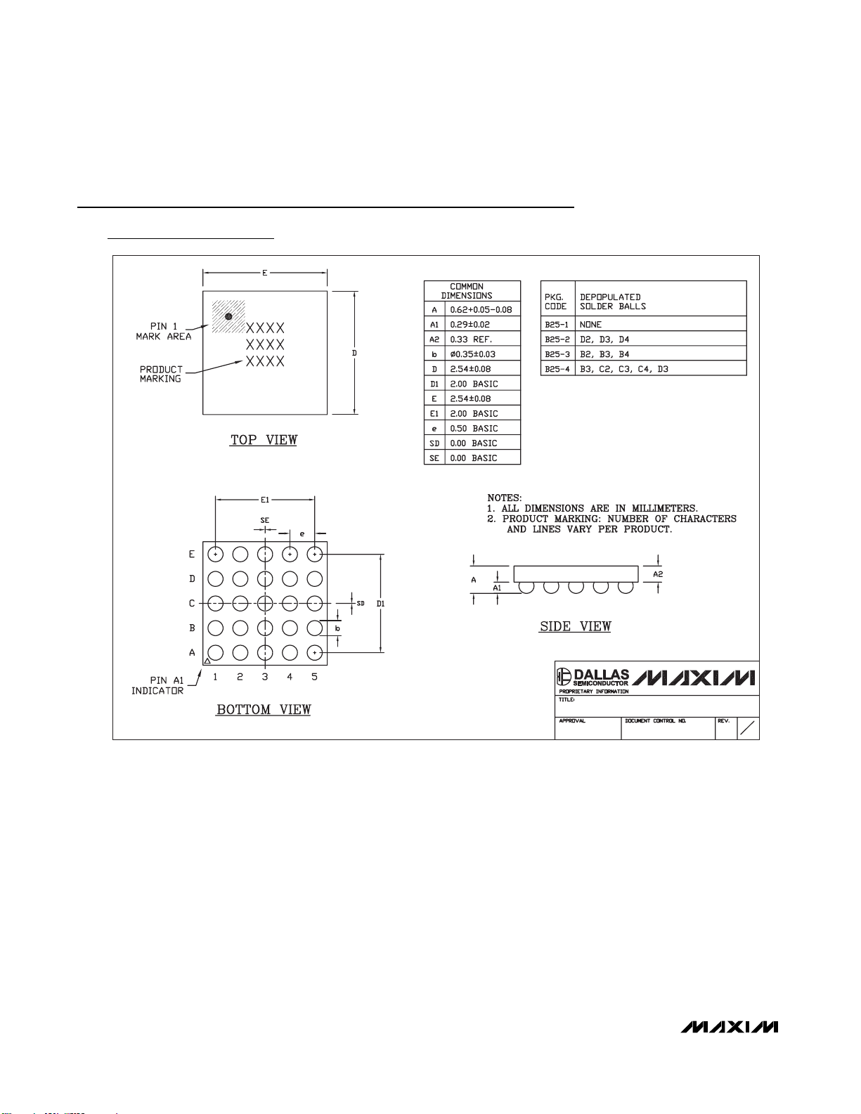
Package Information
(The package drawing(s) in this data sheet may not reflect the most current specifications. For the latest package outline information
go to www.maxim-ic.com/packages
.)
25L, UCSP.EPS
PACKAGE OUTLINE, 5x5 UCSP
21-0096
1
H
1
Page 13
MAX4947/MAX4948
Hex SPDT Data Switch
Maxim cannot assume responsibility for use of any circuitry other than circuitry entirely embodied in a Maxim product. No circuit patent licenses are
implied. Maxim reserves the right to change the circuitry and specifications without notice at any time.
Maxim Integrated Products, 120 San Gabriel Drive, Sunnyvale, CA 94086 408-737-7600 ____________________
13
© 2007 Maxim Integrated Products is a registered trademark of Maxim Integrated Products, Inc.
Package Information (continued)
(The package drawing(s) in this data sheet may not reflect the most current specifications. For the latest package outline information
go to www.maxim-ic.com/packages
.)
Revision History
Pages changed at Rev 1: 1.
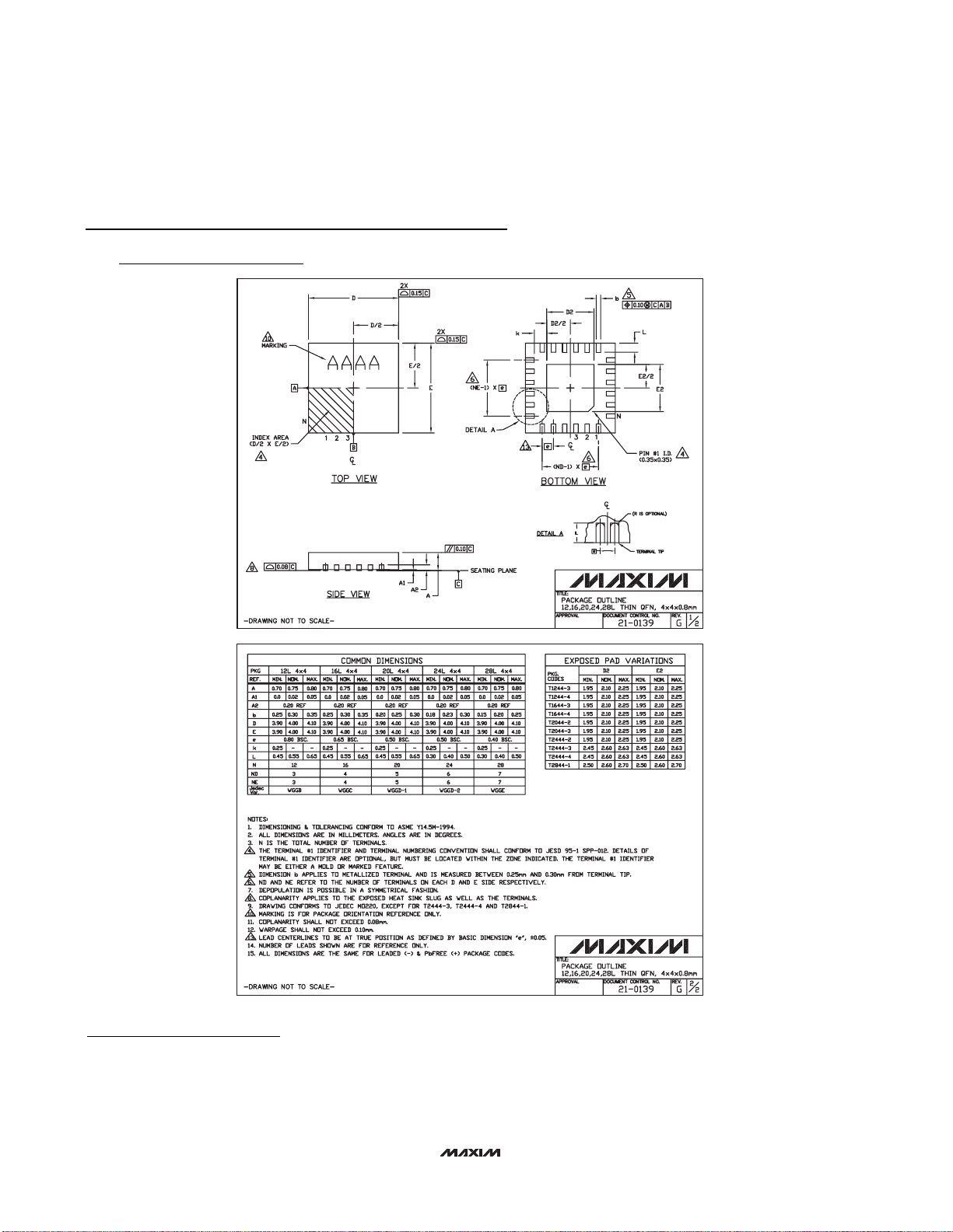
24L QFN THIN.EPS
 Loading...