

19-5541; Rev 1; 3/11
Octal High-Voltage Transmit/Receive Switches
General Description
The MAX4936–MAX4939 are octal, high-voltage, transmit/
receive (T/R) switches. The T/R switches are based on
a diode bridge topology, and the amount of current
in the diode bridges can be programmed through an
SPIK interface. All devices feature a latch-clear input
to asynchronously turn off all T/R switches and put the
device into a low-power shutdown mode. The MAX4936/
MAX4938 include the T/R switch and grass-clipping
diodes, performing both transmit and receive operations.
The MAX4937/MAX4939 include just the T/R switch and
perform the receive operation only.
The MAX4936/MAX4938 transmit path is low impedance
during high-voltage transmit and high impedance during
low-voltage receive, providing isolation between transmit
and receive circuitry. The high-voltage transmit path is
high bandwidth, low distortion, and low jitter.
The receive path for all devices is low impedance during low-voltage receive and high impedance during
high-voltage transmit, providing protection to the receive
circuitry. The low-voltage receive path is high bandwidth,
low noise, low distortion, and low jitter. Each T/R switch
can be individually programmed on or off, allowing these
devices to also be used as receive path multiplexers.
The MAX4936/MAX4937 feature clamping diodes to
protect the receiver input from voltage spikes due to
leakage currents flowing through the T/R switches during transmission. The MAX4938/MAX4939 do not have
clamping diodes and rely on clamping diodes integrated
in the receiver front end.
All devices are available in a small, 56-pin, 5mm x 11mm
TQFN package, and are specified over the commercial
0NC to +70NC temperature range.
Ordering Information/Selector Guide
Features
S Low Power: Low Impedance (5ω) with 1.5mA Bias
Current Only
S Low Noise < 0.5nV/√Hz (typ) with 1.5mA Bias
Current Only
S Wide -3dB Bandwidth 65MHz (typ)
S Easy Programming with SPI Interface
S High Density (8 Channels per Package)
S Grass-Clipping Diodes with Low-Voltage Isolation
(MAX4936/MAX4938)
S Output Clamp Diodes for Receiver Protection
(MAX4936/MAX4937)
S Global Shutdown Control (CLR)
S Each T/R Switch Can Be Individually Programmed
On or Off
S Low-Voltage Receive Path with High-Voltage
Protection
S Space-Saving, 5mm x 11mm, 56-Pin TQFN Package
Applications
Medical/Industrial Imaging
Ultrasound
High-Voltage Transmit and Low-Voltage Isolation
MAX4936–MAX4939
PART
MAX4936CTN+ Yes Yes Yes
MAX4937CTN+ No Yes Yes
MAX4938CTN+** Yes Yes No
MAX4939CTN+** No Yes No
+Denotes a lead(Pb)-free/RoHS-compliant package.
*EP = Exposed pad.
**Future product—contact factory for availability.
SPI is a trademark of Motorola, Inc.
LOW-VOLTAGE
ISOLATION
_______________________________________________________________ Maxim Integrated Products 1
HIGH-VOLTAGE
PROTECTION
OUTPUT CLAMP TEMP RANGE PIN-PACKAGE
0NC to +70NC
0NC to +70NC
0NC to +70NC
0NC to +70NC
56 TQFN-EP*
56 TQFN-EP*
56 TQFN-EP*
56 TQFN-EP*
For pricing, delivery, and ordering information, please contact Maxim Direct at 1-888-629-4642,
or visit Maxim’s website at www.maxim-ic.com.
Octal High-Voltage Transmit/Receive Switches
ABSOLUTE MAXIMUM RATINGS
(All voltages referenced to GND, unless otherwise noted.)
VDD Positive Supply Voltage ...................................-0.3V to +6V
VCC, LVCC_ Positive Supply Voltage ....................-0.3V to +6V
VEE, LVEE_ Negative Supply Voltage ....................-6V to +0.3V
CLK, DIN, CLR, LE Input Voltage ..........................-0.3V to +6V
DOUT Output Voltage ..............................-0.3V to (V
DD
+ 0.3V)
HV_ Input Voltage (MAX4936/MAX4938) ..........-120V to +120V
COM_ Input/Output Voltage ............................... -120V to +120V
NO_ Output Voltage (MAX4936/MAX4937) ...................... Q1.5V
NO_ Output Voltage (MAX4938/MAX4939) ......................... Q6V
Voltage Difference Across Any or
All HV_ (MAX4936/MAX4938) ...................................... Q230V
Stresses beyond those listed under “Absolute Maximum Ratings” may cause permanent damage to the device. These are stress ratings only, and functional
operation of the device at these or any other conditions beyond those indicated in the operational sections of the specifications is not implied. Exposure to absolute
maximum rating conditions for extended periods may affect device reliability.
PACKAGE THERMAL CHARACTERISTICS (Note 1)
MAX4936–MAX4939
TQFN
Junction-to-Ambient Thermal Resistance (qJA) ...........44°C/W
Junction-to-Case Thermal Resistance (qJC) ................. 10°C/W
Note 1: Package thermal resistance were obtained using the method described in JEDEC specification JESD51-7, using a four-
layer board. For detailed information on package thermal considerations, refer to www.maxim-ic.com/thermal-tutorial.
Voltage Difference Across Any or All COM_ .................. Q230V
Continuous Current (HV_ to COM_ ) (MAX4936/MAX4938) ..Q250mA
Continuous Current (Any Other Terminal) ..................... Q100mA
Peak Current (HV_ to COM_ ) (MAX4936/MAX4938)
(Pulsed at 1ms, 0.1% Duty Cycle) ................................ Q2.5A
Continuous Power Dissipation (TA = +70NC)
TQFN (derate 41.0mW/NC above +70NC) .................3279mW
Operating Temperature Range ............................. 0NC to +70NC
Storage Temperature Range ............................ -65NC to +150NC
Junction Temperature ................................................... +150NC
Lead Temperature (soldering, 10s) ................................+300NC
Soldering Temperature (reflow) ......................................+260NC
ELECTRICAL CHARACTERISTICS
(VDD = +1.62V to +5.5V, VCC = +2.7V to +5.5V, VEE = -2.7V to -5.5V, V
unless otherwise noted. Typical values are at TA = +25NC.) (Note 2)
PARAMETER SYMBOL CONDITIONS MIN TYP MAX UNITS
STATIC CHARACTERISTICS
HV_ Input Voltage Range V
|Difference Across Any or All
HV_ |
COM_ Output Voltage Range V
COM_ Input Voltage Range V
|Difference Across Any or All
COM_ |
NO_ Output Voltage Range V
HV_ to COM_ Continuous
Current
HV_ to COM_ Drop V
Diode Bridge Voltage Offset V
IRHV_
ORCM_
IRCM_
ORNO_
I
CN_
CN_
OFF_
MAX4936/MAX4938 only -115 +115 V
MAX4936/MAX4938 only 220 V
|V
| R +2V, I
HV_
= Q100mA (MAX4936/
HV_
MAX4938 only)
V
CC
= +5V, V
= -5V, |V
EE
RL = 200I, CL = 30pF, I
(MAX4936/MAX4937 only)
V
CC
= +5V, V
= -5V, |V
EE
RL = 200I, CL = 30pF, I
V
= 0V (MAX4936/MAX4938 only) -200 +200 mA
COM_
V
COM_
= 0V, I
CN_
= Q2A
(MAX4936/MAX4938 only)
V
= +5V, V
CC
= -5V, COM_ = unconnected,
EE
NO_ = unconnected, ICH = 1.5mA
= 0V, LVCC_ = VCC, LVEE_ = VEE, TA = T
CLR
V
HV_
- 1
V
HV_
0.85
-115 +115 V
| R +2V,
COM_
CH_
COM_
CH_
= 10mA
| < +0.4V,
= 1.5mA
-1
V
COM_
- 0.2
Q0.75
V
COM_
Q 0.1
Q2
-200 +200 mV
Q
V
to T
MIN
V
HV_
+ 1
220 V
+1
COM_
+ 0.2
MAX
V
V
V
,
2 ______________________________________________________________________________________
Octal High-Voltage Transmit/Receive Switches
ELECTRICAL CHARACTERISTICS (continued)
(VDD = +1.62V to +5.5V, VCC = +2.7V to +5.5V, VEE = -2.7V to -5.5V, V
unless otherwise noted. Typical values are at TA = +25NC.) (Note 2)
PARAMETER SYMBOL CONDITIONS MIN TYP MAX UNITS
HV_ Off-Leakage Current I
LHV_
- V
HV_
(MAX4936/MAX4938 only)
|V
- V
HV_
COM_
COM_
| < +0.3V, V
| < +0.3V, V
|V
switch is off (MAX4936/MAX4938 only)
COM_ Off-Leakage Current I
LCOM_
HV_ = unconnected, switch is off
(MAX4936/MAX4938 only)
Switch is off (MAX4937/MAX4939 only) -1 +1
|V
| < +0.3V,
NO_ Off-Leakage Current I
LNO_
NO_
switch is off
DYNAMIC CHARACTERISTICS
V
= +5V, VEE = -5V, RL = 200I,
Diode Bridge Turn-On Time t
ON
CC
ICH = 1.5mA, CL = 30pF, V
Figure 1
V
= +5V, VEE = -5V, RL = 200I,
Diode Bridge Turn-Off Time t
OFF
CC
ICH = 1.5mA, CL = 30pF, V
Figure 1
Reverse Recovery Time t
SPI Power-Up Delay t
Small-Signal COM_ to NO_ On
Impedance
R
RR
DLY
ICOM_
I
= I
FWD
V
CC
= 10mA 450 ns
RVR
= +5V, VEE = -5V, V
ICH = 1.5mA, f = 5MHz
COM_ to NO_, switch is on,
-3dB Bandwidth BW
|V
COM_
| < +0.4V, V
RL = 200I, CL = 30pF, ICH = 1.5mA
= 0V, LVCC_ = VCC, LVEE_ = VEE, TA = T
CLR
= 0V
COM_
HV_
= 0V,
-3 +3
-3 +3
-1 +1
MAX4936/MAX4937 -2 +2
MAX4938/MAX4939 -1 +1
COM_
COM_
= Q0.4V,
= Q0.4V,
200 ns
500
= 0V,
NO_
= +5V, VEE = -5V,
CC
4.5
65 MHz
5
MIN
to T
MAX
FA
FA
FA
FA
FA
ms
Fs
I
MAX4936–MAX4939
,
Off-Isolation V
Crosstalk V
_______________________________________________________________________________________ 3
ISO
CT
HV_ to COM_, |V
V
= +5V, VEE = -5V, RL = 100I,
CC
HV_
- V
COM_
| < +0.3V,
CL = 100pF, f = 1MHz
(MAX4936/MAX4938 only)
COM_ to NO_, switch is off, V
CC
= +5V,
VEE = -5V, RL = 200I, CL = 30pF, f = 1MHz
Between any two HV_ to COM_ channels,
|V
| R +2V, V
HV_
CC
= +5V,
VEE = -5V, RL = 100I, CL = 100pF,
f = 5MHz (MAX4936/MAX4938 only)
Between any two COM_ to NO_ channels,
switch is on, |V
COM_
| < +0.4V, V
CC
= +5V,
VEE = -5V, RL = 200I, CL = 30pF,
ICH = 1.5mA, f = 5MHz
-50
dB
-75
-60
dB
-71
Octal High-Voltage Transmit/Receive Switches
ELECTRICAL CHARACTERISTICS (continued)
(VDD = +1.62V to +5.5V, VCC = +2.7V to +5.5V, VEE = -2.7V to -5.5V, V
unless otherwise noted. Typical values are at TA = +25NC.) (Note 2)
PARAMETER SYMBOL CONDITIONS MIN TYP MAX UNITS
HV_ to COM_, |V
VEE = -5V, RL = 100I, CL = 100pF,
f = 5MHz (MAX4936/MAX4938 only)
2nd Harmonic Distortion HD2
COM_ to NO_, switch is on, |V
V
= +5V, VEE = -5V, RL = 200I,
CC
CL = 30pF, ICH = 1.5mA, f = 5MHz
HV_ to COM_, |V
VEE = -5V, RL = 100I, CL = 100pF,
f = 5MHz (MAX4936/MAX4938 only)
3rd Harmonic Distortion HD3
COM_ to NO_, switch is on, |V
V
= +5V, VEE = -5V, RL = 200I,
CC
MAX4936–MAX4939
CL = 30pF, ICH = 1.5mA, f = 5MHz
COM_ to NO_, switch is on,
Two-Tone Intermodulation
Distortion (Note 3)
IMD3
|V
| < +0.4V, V
COM_
RL = 200I, CL = 30pF, ICH = 1.5mA,
f1 = 5MHz, f2 = 5.01MHz
|V
- V
HV_
HV_
- V
COM_
COM_
HV_ Off Capacitance C
COM_ Off Capacitance C
HV_(OFF)
COM_(OFF)
(MAX4936/MAX4938 only)
|V
(MAX4936/MAX4938 only)
Switch is off (MAX4937/MAX4939 only) 12
NO_ On Capacitance C
NO_ Off Capacitance C
NO_(ON)
NO_(OFF)
|V
| < +0.4V, switch is on 20 pF
NO_
|V
| < +0.4V, switch is off 7.5 pF
NO_
DIGITAL I/Os (CLR, DIN, DOUT, CLK, LE)
Input High Voltage V
IH
VDD = +2.25V to +5.5V
VDD = +1.62V to +1.98V 1.4
Input Low Voltage V
Input Hysteresis V
Input Leakage Current I
Input Capacitance C
DOUT Low Voltage V
DOUT High Voltage V
IL
HYST
IL
IN
OL
OH
VDD = +2.25V to +5.5V 0.6
VDD = +1.62V to +1.98V 0.4
VDD = +3V 50
VDD = +1.8V 90
CLR, DIN, CLK, LE = GND or V
I
= 5mA 0.4 V
SINK
I
SOURCE
= 5mA
POWER SUPPLY (VDD, VCC, VEE)
Positive Logic Supply Voltage V
Positive Analog Supply Voltage V
Negative Analog Supply
Voltage
DD
CC
V
EE
COM_
COM_
| < +0.3V
| < +0.3V, switch is off
= 0V, LVCC_ = VCC, LVEE_ = VEE, TA = T
CLR
| R +2V, V
| R +2V, V
= +5V, VEE = -5V,
CC
COM_
COM_
= +5V,
CC
| < +0.4V,
= +5V,
CC
| < +0.4V,
V
-
DD
0.5
DD
-1 +1
V
-
DD
0.4
+1.62 +5.5 V
+2.7 +5.5 V
-5.5 -2.7 V
MIN
-90
-95
-90
-115
-77 dBc
12 pF
17
5 pF
to T
MAX
dBc
dBc
pF
V
V
mV
FA
V
,
4 ______________________________________________________________________________________
Octal High-Voltage Transmit/Receive Switches
ELECTRICAL CHARACTERISTICS (continued)
(VDD = +1.62V to +5.5V, VCC = +2.7V to +5.5V, VEE = -2.7V to -5.5V, V
unless otherwise noted. Typical values are at TA = +25NC.) (Note 2)
PARAMETER SYMBOL CONDITIONS MIN TYP MAX UNITS
Positive Logic Supply Current I
Positive Analog Supply Current I
Positive Analog Shutdown
Supply Current
I
CC_SHDN
Negative Analog Supply
Current
Negative Analog Shutdown
Supply Current
On Power-Supply Rejection
Ratio
Off Power-Supply Rejection
Ratio
I
EE_SHDN
PSRR
PSRR
I
DD
CC
EE
CLR, DIN, CLK, LE = GND or V
Per channel, switch is on, V
VEE = -5V, ICH = 1.5mA
CLR = high +1
Per channel, switch is on, V
VEE = -5V, ICH = 1.5mA
CLR = high -1
VCC to NO_ or VEE to NO_, switch is on,
V
ON
= +5V, VEE = -5V, RL = 200I,
CC
CL = 30pF, ICH = 1.5mA, f = 1MHz
VCC to NO_ or VEE to NO_, switch is off,
V
OFF
= +5V, VEE = -5V, RL = 200I,
CC
CL = 30pF, f = 1MHz
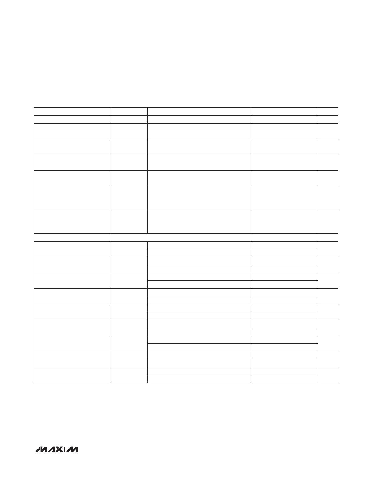
LOGIC TIMING (CLR, DIN, DOUT, CLK, LE) (Figure 1)
V
= 3V Q10%
CLK Period t
CLK High Time t
CLK Low Time t
CLK to DOUT Delay t
DIN to CLK Setup Time t
DIN to CLK Hold Time t
CLK to LE Setup Time
LE Low Pulse Width
CLR High Pulse Width t
t
t
CP
CH
CL
DO
DS
DH
CS
WL
WC
DD
V
= 1.8V Q10%
DD
V
= 3V Q10%
DD
V
= 1.8V Q10%
DD
V
= 3V Q10%
DD
V
= 1.8V Q10%
DD
V
= 3V Q10%, CL P 20pF
DD
V
= 1.8V Q10%, CL P 20pF
DD
V
= 3V Q10%
DD
V
= 1.8V Q10%
DD
V
= 3V Q10%
DD
V
= 1.8V Q10%
DD
V
= 3V Q10%
DD
V
= 1.8V Q10%
DD
V
= 3V Q10%
DD
V
= 1.8V Q10%
DD
V
= 3V Q10%
DD
V
= 1.8V Q10%
DD
Note 2: All specifications are 100% production tested at TA = +70NC, unless otherwise noted. Specifications at 0NC are guaran-
teed by design.
Note 3: See the Ultrasound-Specific IMD3 Specification section.
= 0V, LVCC_ = VCC, LVEE_ = VEE, TA = T
CLR
DD
= +5V,
CC
CC
= +5V,
+1.15 +1.5 +2 mA
-2 -1.5 -1.15 mA
-77 dB
-80 dB
50
100
20
45
20
45
3 30
7 70
10
16
4
4
36
65
14
22
20
40
+1
MIN
to T
FA
FA
FA
MAX
ns
ns
ns
ns
ns
ns
ns
ns
ns
MAX4936–MAX4939
,
_______________________________________________________________________________________ 5
Octal High-Voltage Transmit/Receive Switches
OFF
D
N + 1
ON
DIN
LE
CLK
DOUT
T/R SWITCH
MAX4936–MAX4939
CLR
t
WC
Figure 1. Serial Interface Timing
50%
50%
D
N
50%
t
DS
50%50%
50%
t
WL
50%
t
CS
t
DH
t
DO
50%
t
OFF
90%
50%
10%
D
N - 1
t
ON
6 ______________________________________________________________________________________

Octal High-Voltage Transmit/Receive Switches
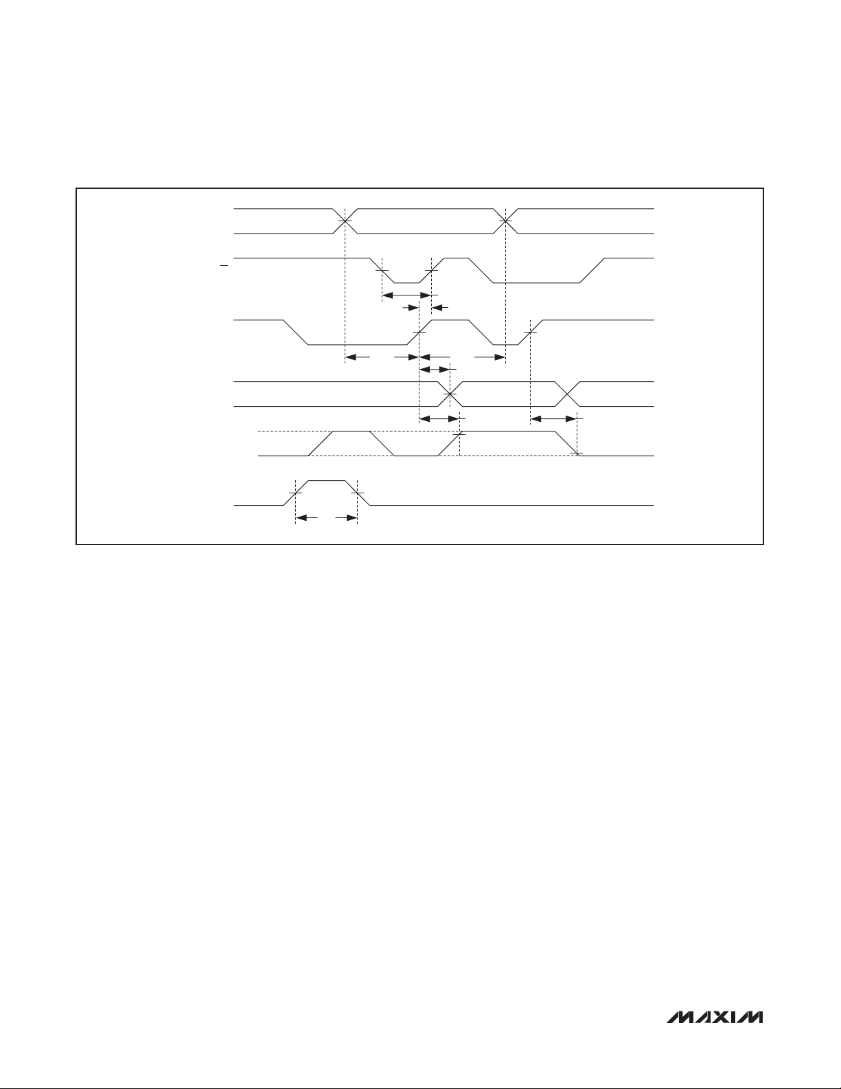
Typical Operating Characteristics
(V
= +3V, V
DD
wise noted.)
CC
= +5V, V
= -5V, ICH = 1.5mA, R
EE
COM_
= 200I, R
= 200I, f = 5MHz, V
NO_
= 0V, TA = +25NC, unless other-
CLR
MAX4936–MAX4939
ICC, IEE SUPPLY CURRENT
, VEE SUPPLY VOLTAGE
vs. V
2.0
1.5
1.0
SUPPLY CURRENT (mA)
EE
I
,
0.5
CC
I
0
I
CC_SHDN
CC
ONE CHANNEL ON
3.02.5
VCC, VEE SUPPLY VOLTAGE (V)
, I
EE_SHDN
vs. TEMPERATURE
0.20
0.15
0.10
SHUTDOWN CURRENT (µA)
EE_SHDN
0.05
, I
MAX4936-39 toc01
5.55.04.54.03.5
SUPPLY SHUTDOWN CURRENT
MAX4936-39 toc03
ICC, IEE SUPPLY CURRENT
vs. TEMPERATURE
2.00
ONE CHANNEL ON
1.75
1.50
SUPPLY CURRENT (mA)
EE
, I
1.25
CC
I
1.00
-40 85
TEMPERATURE (°C)
COM_ TO NO_ SMALL-SIGNAL TRANSFER
FUNCTION vs. FREQUENCY
0
R
= 50Ω
NO_
-0.5
-1.0
COM_ TO NO_ ATTENUATION (dB)
ICH = 1.5mA
ICH = 3mA
MAX4936-39 toc02
603510-15
MAX4936-39 toc04
CC_SHDN
I
0
0 70
TEMPERATURE (°C)
56422814
COM_ TO NO_ IMPEDANCE
vs. FREQUENCY
9
8
7
ICH = 1.5mA
6
5
4
3
2
COM_ TO NO_ IMPEDANCE (Ω)
1
0
0 20
ICH = 3mA
15105
FREQUENCY (MHz)
MAX4936-39 toc05
-1.5
0 20
FREQUENCY (MHz)
COM_ TO NO_ CROSSTALK
vs. FREQUENCY
-60
R
= 200Ω
NO_
= 200Ω
R
COM_
-70
-80
CROSSTALK (dB)
-90
-100
1 10
FREQUENCY (MHz)
15105
MAX4936-39 toc06
_______________________________________________________________________________________ 7
Octal High-Voltage Transmit/Receive Switches
Typical Operating Characteristics (continued)
(V
= +3V, V
DD
wise noted.)
CC
= +5V, V
= -5V, ICH = 1.5mA, R
EE
COM_
= 200I, R
= 200I, f = 5MHz, V
NO_
= 0V, TA = +25NC, unless other-
CLR
-70
R
= 200Ω
NO_
R
= 200Ω
COM_
PSRR_V
-75
PSRR (dB)
-80
PSRR_V
MAX4936–MAX4939
-85
1 10
FREQUENCY (MHz)
EE
CC
HV_/COM_ vs. TIME
COM_LOAD = 100Ω 100pF
MAX4936-39 toc07
VOLTAGE (V)
MAX4936-39 toc10
0.08
0.06
0.04
0.02
-0.02
-0.04
-0.06
-0.08
PSRR vs. FREQUENCY
COM_/NO_ SMALL SIGNAL vs. TIME
(2MHz GAUSSIAN SIGNAL AT COM_)
R
= 50Ω
NO_
0
-5 5
COM_
NO_
TIME (ms)
FOR CLR TOGGLING FROM V
V
HV_
50V/div
MAX4936-39 toc08
-20
-40
COM_/NO_ FET (dB)
-60
43-4 -3 -2 0 1-1 2
-80
COM_/NO_ vs. TIME
NO_LOAD = 200Ω 30pF
COM_/NO_ FFT vs. FREQUENCY
(2MHz GAUSSIAN SIGNAL AT COM_)
0
0 15
DD
COM_LOAD = 200Ω
NO_
COM_
FREQUENCY (MHz)
TO GND TO V
MAX4936-39 toc11
DD
V
COM_
5mV/div
R
= 50Ω
NO_
105
MAX4936-39 toc09
V
COM_
50V/div
100ns/div
200µs/div
8 ______________________________________________________________________________________
V
NO_
5mV/div

Octal High-Voltage Transmit/Receive Switches
Pin Configuration
TOP VIEW
NO5
LVCC5
GND
NO5
HV5
LVCC5
LVEE6
COM5
LVEE6
NO6
N.C.
NO6
LVCC6
HV6
LVCC6
LVEE7
COM6
LVEE7
NO7
N.C.
NO7
*EP
LVCC7
HV7
LVCC7
LVEE8
COM7
LVEE8
28
NO8
27
LVCC8
DOUT
26
DIN
25
CLK
24
GND
23
COM8
22
HV8
21
NO1
LVCC1
CLR
GND
N.C.
COM1
HV1
LVEE5
LVEE4
NO4
LVCC4
LVEE3
NO3
LVCC3
LVEE2
NO2
LVCC2
LVEE1
48 47 46 45 44 43
49
50
LE
51
52
53
54
55
56
1+2 3 4 5 6 7 8 9 10 11 12 13 14 15 16 17 18 19 20
N.C.
NO2
COM3
LVEE2
HV3
LVCC3
N.C.
NO3
HV2
COM2
LVCC2
LVEE1
48 47 46 45 44 43
40 39 38 37 36 35 34 33 32 31 30 29
42 41
MAX4936/MAX4938
EE
DD
V
VCCV
HV4
COM4
LVEE5
LVEE4
NO4
LVCC4
LVEE3
40 39 38 37 36 35 34 33 32 31 30 29
42 41
MAX4936–MAX4939
NO8
*EP
N.C.
COM7
28
LVCC8
27
DOUT
26
DIN
25
CLK
24
GND
23
COM8
22
N.C.
21
NO1
LVCC1
CLR
GND
N.C.
COM1
N.C.
49
50
LE
51
52
53
54
55
56
1+2 3 4 5 6 7 8 9 10 11 12 13 14 15 16 17 18 19 20
N.C.
N.C.
N.C.
COM2
COM3
MAX4937/MAX4939
N.C.
N.C.
COM4
EE
DD
V
VCCV
GND
N.C.
COM5
N.C.
N.C.
COM6
N.C.
TQFN
*CONNECT EP TO GND.
(5mm × 11mm)
Pin Description
PIN
MAX4936/
MAX4938
MAX4937/
MAX4939
1 1 COM2
2 — HV2
NAME FUNCTION
T/R Switch 2 Input. When the switch is on, low-voltage signals are passed
through from COM2 to NO2, while high-voltage signals are blocked. When the
switch is off, both low-voltage and high-voltage signals are blocked.
T/R Switch 2 Input. COM2 follows HV2 when high-voltage signals are present on
HV2. HV2 is isolated from COM2 when low-voltage signals are present on COM2.
_______________________________________________________________________________________ 9

Octal High-Voltage Transmit/Receive Switches
Pin Description (continued)
PIN
MAX4936/
MAX4938
3, 6, 15, 18, 54
4 4 COM3
5 — HV3
7 7 COM4
MAX4937/
MAX4939
2, 3, 5, 6, 8,
13, 15, 16, 18,
19, 21, 54, 56
MAX4936–MAX4939
8 — HV4
9 9 V
10 10 V
11 11 V
12, 23, 53 12, 23, 53 GND Ground
13 — HV5
14 14 COM5
16 — HV6
17 17 COM6
19 — HV7
20 20 COM7
21 — HV8
22 22 COM8
NAME FUNCTION
N.C. No Connection. Not internally connected.
T/R Switch 3 Input. When the switch is on, low-voltage signals are passed
through from COM3 to NO3, while high-voltage signals are blocked. When the
switch is off, both low-voltage and high-voltage signals are blocked.
T/R Switch 3 Input. COM3 follows HV3 when high-voltage signals are present on
HV3. HV3 is isolated from COM3 when low-voltage signals are present on COM3.
T/R Switch 4 Input. When the switch is on, low-voltage signals are passed
through from COM4 to NO4, while high-voltage signals are blocked. When the
switch is off, both low-voltage and high-voltage signals are blocked.
T/R Switch 4 Input. COM4 follows HV4 when high-voltage signals are present on
HV4. HV4 is isolated from COM4 when low-voltage signals are present on COM4.
Positive Logic Supply. Bypass VDD to GND with a 1FF or greater ceramic
DD
capacitor as close as possible to the device.
Positive Analog Supply. Bypass VCC to GND with a 1FF or greater ceramic
CC
capacitor as close as possible to the device.
Negative Analog Supply. Bypass VEE to GND with a 1FF or greater ceramic
EE
capacitor as close as possible to the device.
T/R Switch 5 Input. COM5 follows HV5 when high-voltage signals are present on
HV5. HV5 is isolated from COM5 when low-voltage signals are present on COM5.
T/R Switch 5 Input. When the switch is on, low-voltage signals are passed
through from COM5 to NO5, while high-voltage signals are blocked. When the
switch is off, both low-voltage and high-voltage signals are blocked.
T/R Switch 6 Input. COM6 follows HV6 when high-voltage signals are present on
HV6. HV6 is isolated from COM6 when low-voltage signals are present on COM6.
T/R Switch 6 Input. When the switch is on, low-voltage signals are passed
through from COM6 to NO6, while high-voltage signals are blocked. When the
switch is off, both low-voltage and high-voltage signals are blocked.
T/R Switch 7 Input. COM7 follows HV7 when high-voltage signals are present on
HV7. HV7 is isolated from COM7 when low-voltage signals are present on COM7.
T/R Switch 7 Input. When the switch is on, low-voltage signals are passed
through from COM7 to NO7, while high-voltage signals are blocked. When the
switch is off, both low-voltage and high-voltage signals are blocked.
T/R Switch 8 Input. COM8 follows HV8 when high-voltage signals are present on
HV8. HV8 is isolated from COM8 when low-voltage signals are present on COM8.
T/R Switch 8 Input. When the switch is on, low-voltage signals are passed
through from COM8 to NO8, while high-voltage signals are blocked. When the
switch is off, both low-voltage and high-voltage signals are blocked.
10 _____________________________________________________________________________________

Octal High-Voltage Transmit/Receive Switches
Pin Description (continued)
PIN
MAX4936/
MAX4938
24 24 CLK Serial-Clock Input
25 25 DIN Serial-Data Input
26 26 DOUT Serial-Data Output
27 27 LVCC8
28 28 NO8
29 29 LVEE8
30 30 LVCC7
31 31 NO7
32 32 LVEE7
33 33 LVCC6
34 34 NO6
35 35 LVEE6
36 36 LVCC5
37 37 NO5
38 38 LVEE5
39 39
40 40 NO4
MAX4937/
MAX4939
NAME FUNCTION
Inductor VCC Connection. Connect an inductor between LVCC8 and VCC to
improve noise performance, otherwise connect LVCC8 to VCC.
T/R Switch 8 Output. When the switch is on, low-voltage signals are passed
through from COM8 to NO8, while high-voltage signals are blocked. When the
switch is off, both low-voltage and high-voltage signals are blocked. NO8 is
limited with clamping diodes on MAX4936/MAX4937.
Inductor VEE Connection. Connect an inductor between LVEE8 and VEE to
improve noise performance; otherwise, connect LVEE8 to VEE.
Inductor VCC Connection. Connect an inductor between LVCC7 and VCC to
improve noise performance; otherwise, connect LVCC7 to VCC.
T/R Switch 7 Output. When the switch is on, low-voltage signals are passed
through from COM7 to NO7, while high-voltage signals are blocked. When the
switch is off, both low-voltage and high-voltage signals are blocked. NO7 is
limited with clamping diodes on MAX4936/MAX4937.
Inductor VEE Connection. Connect an inductor between LVEE7 and VEE to
improve noise performance; otherwise, connect LVEE7 to VEE.
Inductor VCC Connection. Connect an inductor between LVCC6 and VCC to
improve noise performance; otherwise, connect LVCC6 to VCC.
T/R Switch 6 Output. When the switch is on, low-voltage signals are passed
through from COM6 to NO6, while high-voltage signals are blocked. When the
switch is off, both low-voltage and high-voltage signals are blocked. NO6 is
limited with clamping diodes on MAX4936/MAX4937.
Inductor VEE Connection. Connect an inductor between LVEE6 and VEE to
improve noise performance; otherwise, connect LVEE6 to VEE.
Inductor VCC Connection. Connect an inductor between LVCC5 and VCC to
improve noise performance; otherwise, connect LVCC5 to VCC.
T/R Switch 5 Output. When the switch is on, low-voltage signals are passed
through from COM5 to NO5, while high-voltage signals are blocked. When the
switch is off, both low-voltage and high-voltage signals are blocked. NO5 is
limited with clamping diodes on MAX4936/MAX4937.
Inductor VEE Connection. Connect an inductor between LVEE5 and VEE to
improve noise performance; otherwise, connect LVEE5 to VEE.
LVEE4
Inductor VEE Connection. Connect an inductor between LVEE4 and VEE to
improve noise performance; otherwise, connect LVEE4 to VEE.
T/R Switch 4 Output. When the switch is on, low-voltage signals are passed
through from COM4 to NO4, while high-voltage signals are blocked. When the
switch is off, both low-voltage and high-voltage signals are blocked. NO4 is
limited with clamping diodes on MAX4936/MAX4937.
MAX4936–MAX4939
______________________________________________________________________________________ 11
Octal High-Voltage Transmit/Receive Switches
Pin Description (continued)
PIN
MAX4936/
MAX4938
41 41 LVCC4
42 42 LVEE3
43 43 NO3
44 44 LVCC3
MAX4936–MAX4939
45 45 LVEE2
46 46 NO2
47 47 LVCC2
48 48 LVEE1
49 49 NO1
50 50 LVCC1
51 51
52 52 CLR
55 55 COM1
56 — HV1
— — EP
MAX4937/
MAX4939
NAME FUNCTION
Inductor VCC Connection. Connect an inductor between LVCC4 and VCC to
improve noise performance; otherwise, connect LVCC4 to VCC.
Inductor VEE Connection. Connect an inductor between LVEE3 and VEE to
improve noise performance; otherwise, connect LVEE3 to VEE.
T/R Switch 3 Output. When the switch is on, low-voltage signals are passed
through from COM3 to NO3, while high-voltage signals are blocked. When the
switch is off, both low-voltage and high-voltage signals are blocked. NO3 is
limited with clamping diodes on MAX4936/MAX4937.
Inductor VCC Connection. Connect an inductor between LVCC3 and VCC to
improve noise performance; otherwise, connect LVCC3 to VCC.
Inductor VEE Connection. Connect an inductor between LVEE2 and VEE to
improve noise performance; otherwise, connect LVEE2 to VEE.
T/R Switch 2 Output. When the switch is on, low-voltage signals are passed
through from COM2 to NO2, while high-voltage signals are blocked. When the
switch is off, both low-voltage and high-voltage signals are blocked. NO2 is
limited with clamping diodes on MAX4936/MAX4937.
Inductor VCC Connection. Connect an inductor between LVCC2 and VCC to
improve noise performance; otherwise, connect LVCC2 to VCC.
Inductor VEE Connection. Connect an inductor between LVEE1 and VEE to
improve noise performance; otherwise, connect LVEE1 to VEE.
T/R Switch 1 Output. When the switch is on, low-voltage signals are passed
through from COM1 to NO1, while high-voltage signals are blocked. When the
switch is off, both low-voltage and high-voltage signals are blocked. NO1 is
limited with clamping diodes on MAX4936/MAX4937.
Inductor VCC Connection. Connect an inductor between LVCC1 and VCC to
improve noise performance; otherwise, connect LVCC1 to VCC.
Active-Low Latch-Enable Input. Drive LE low to change the contents of the latch
LE
and update the state of the switches. Drive LE high to hold the contents of the
latch.
Active-High Latch-Clear Input. Drive CLR high to clear the contents of the latch
and disable all the switches. When CLR is driven high, the device enters
shutdown mode. CLR does not affect the contents of the register.
T/R Switch 1 Input. When the switch is on, low-voltage signals are passed
through from COM1 to NO1, while high-voltage signals are blocked. When the
switch is off, both low-voltage and high-voltage signals are blocked.
T/R Switch 1 Input. COM1 follows HV1 when high-voltage signals are present on
HV1. HV1 is isolated from COM1 when low-voltage signals are present on COM1.
Exposed Pad. Internally connected to GND. Connect EP to a large ground plane
to maximize thermal performance. Do not use EP as the only GND connection.
12 _____________________________________________________________________________________
Octal High-Voltage Transmit/Receive Switches
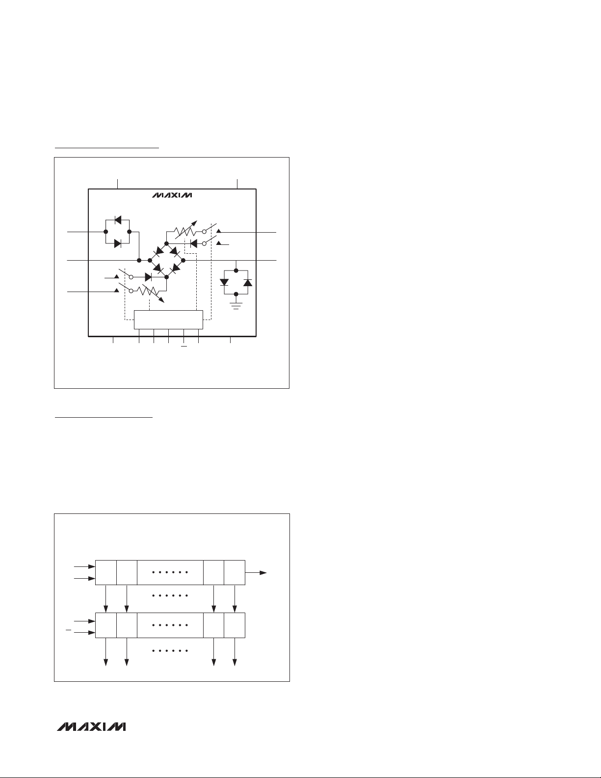
Functional Diagram
V
DD
MAX4936−MAX4939
(SINGLE CHANNEL)
HV_
COM_
V
LVEE_
*LOW-VOLTAGE ISOLATION DIODES AVAILABLE ON MAX4936/MAX4938 ONLY.
**OUTPUT CLAMP DIODES AVAILABLE ON MAX4936/MAX4937 ONLY.
*
CC
SPI LOGIC
GND V
CLK DIN DOUT LE CLR
V
CC
LVCC_
V
EE
NO_
**
EE
Detailed Description
The MAX4936–MAX4939 are octal, high-voltage transmit/receive (T/R) switches. The T/R switches are based
on a diode bridge topology, and the amount of current
in the diode bridges can be programmed through an
SPI interface. All devices feature a latch-clear input to
asynchronously turn off all T/R switches and put the
device into a low-power shutdown mode. The MAX4936/
SPI LOGIC
REGISTER
CLK
DIN
D0 D1 D10 D11
DOUT
MAX4938 include the T/R switch and grass-clipping
MAX4936–MAX4939
diodes, performing both transmit and receive operations.
The MAX4937/MAX4939 include just the T/R switch and
perform the receive operation only.
The MAX4936/MAX4938 transmit path is low impedance
during high-voltage transmit and high impedance during
low-voltage receive, providing isolation between transmit
and receive circuitry. The high-voltage transmit path is
high bandwidth, low distortion, and low jitter.
The receive path for all devices is low impedance during low-voltage receive and high impedance during
high-voltage transmit, providing protection to the receive
circuitry. The low-voltage receive path is high bandwidth,
low noise, low distortion, and low jitter. Each T/R switch
can be individually programmed on or off, allowing these
devices to also be used as receive path multiplexers.
The MAX4936/MAX4937 feature clamping diodes to
protect the receiver input from voltage spikes due to
leakage currents flowing through the T/R switches during transmission. The MAX4938/MAX4939 do not have
clamping diodes and rely on clamping diodes integrated
in the receiver front-end.
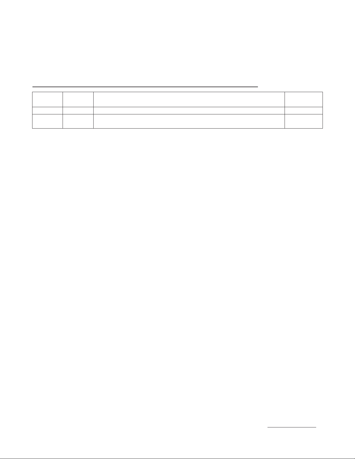
Serial Interface
All the devices are controlled by a serial interface with a
12-bit serial shift register and transparent latch (Figure 2).
Each of the first 4 data bits controls the bias current into
the diode bridges (see Figure 3 and Table 2), while the
remaining 8 data bits control a T/R switch (Table 1). Data
on DIN is clocked with the most significant bit (MSB) first
into the shift register on the rising edge of CLK. Data is
clocked out of the shift register onto DOUT on the rising
edge of CLK. DOUT reflects the status of DIN, delayed
by 12 clock cycles (Figure 4).
Transmit/Receive Switch
The T/R switch is based on a diode bridge topology. The
amount of bias current into each diode bridge is adjustable by setting the S0–S3 switches through the serial
interface (see Figure 3 and Table 2).
CLR
LE
Figure 2. SPI Logic
ON1 ON2 S2 S3
LATCH
Drive LE logic-low to change the contents of the latch
and update the state of the T/R switches (Figure 4).
Drive LE logic-high to hold the contents of the latch and
prevent changes to the switches’ states. To reduce noise
due to clock feedthrough, drive LE logic-high while data
is clocked into the shift register. After the data shift register is loaded with valid data, pulse LE logic-low to load
the contents of the shift register into the latch.
______________________________________________________________________________________ 13
Latch Enable (LE)

Octal High-Voltage Transmit/Receive Switches
LVCC (LVEE)
S3R3S2
R2S1R1S0R0
DIODE BRIDGE
Figure 3. Diode Bias Current Control
LE
MAX4936–MAX4939
CLK
DIN
D11
D10
Latch Clear (CLR)
Drive CLR logic-high to reset the contents of the latch to
zero and open all T/R switches. CLR does not affect the
contents of the shift register. Once CLR is high again,
and LE is driven low, the contents of the shift register are
loaded into the latch.
Power-On Reset
The devices feature a power-on-reset circuit to ensure
all switches are off at power-on. The internal 12-bit serial
shift register and latch are set to zero on power-up.
D9
D1
D0
DOUT
D11'
Figure 4. Latch-Enable Interface Timing
MSB
D10'
D9'
D11'–D0' FROM PREVIOUS DATA
POWER-UP DEFAULT: D11–D0 = 0
D1'
LSB
D0'
D11
14 _____________________________________________________________________________________

Octal High-Voltage Transmit/Receive Switches
Table 1. Serial Interface Programming
DATA BITS
D0
D1 D2 D3 D4 D5 D6 D7 D8 D9 D10
(LSB)
L L L Off
H L L On
L L L Off
H L L On
L L L Off
H L L On
L L L Off
H L L On
L L L Off
H L L On
L L L Off
H L L On
L L L Off
H L L On
L L L Off
H L L On
L L L Off
H L L On
L L L Off
H L L On
L L L Off
H L L On
X X X X X X X X X X X X H L Hold Previous State
X X X X X X X X X X X X X H Off Off Off Off Off Off Off Off Off Off Off Off
L = Low, H = High, X = Don’t care.
CONTROL
D11
(MSB)
BITS
CLR SW1 SW2 SW3 SW4 SW5 SW6 SW7 SW8 S0 S1 S2 S3
LE
L L L Off
H L L On
FUNCTION
MAX4936–MAX4939
Table 2. Diode Bias Current
SWITCHES
RESISTORS (I)
S3 S2 S1 S0 R3 R2 R1 R0
RESISTOR
COMBINATION
(I)
0 0 0 0 350 700 1400 2800 — 0 0
0 0 0 1 350 700 1400 2800 2800 0.78 1.50
0 0 1 0 350 700 1400 2800 1400 1.58 3.00
0 0 1 1 350 700 1400 2800 933 2.36 4.50
0 1 0 0 350 700 1400 2800 700 3.14 6.00
0 1 0 1 350 700 1400 2800 560 3.98 7.50
0 1 1 0 350 700 1400 2800 467 4.72 9.00
0 1 1 1 350 700 1400 2800 400 5.50 10.50
1 0 0 0 350 700 1400 2800 350 6.28 12.00
1 0 0 1 350 700 1400 2800 311 7.08 13.50
1 0 1 0 350 700 1400 2800 280 7.86 15.00
1 0 1 1 350 700 1400 2800 255 8.64 16.50
1 1 0 0 350 700 1400 2800 233 9.42 18.00
1 1 0 1 350 700 1400 2800 215 10.22 19.50
1 1 1 0 350 700 1400 2800 200 11.00 21.00
1 1 1 1 350 700 1400 2800 187 11.78 22.50
*VEE = -V
CC
______________________________________________________________________________________ 15
TYPICAL DIODE BRIDGE CURRENT
(mA) vs. S[3:0] CONTROL BITS (*)
VCC = 3.0V VCC = 5.0V

Octal High-Voltage Transmit/Receive Switches
Applications Information
For medical ultrasound applications, see Figures 5, 6,
and 7.
Ultrasound-Specific IMD3 Specification
Unlike typical communications applications, the two input
tones are not equal in magnitude for the ultrasound-specific IMD3 two-tone specification. In this measurement,
F1 represents reflections from tissue and F2 represents
reflections from blood. The latter reflections are typically
25dB lower in magnitude, and hence the measurement
is defined with one input tone 25dB lower than the other.
The IMD3 product of interest (F1 - (F2 - F1)) presents
itself as an undesired Doppler error signal in ultrasound
applications. See Figure 8.
Logic Levels
The digital interface inputs CLK, DIN, LE, and CLR are
MAX4936–MAX4939
tolerant of up to +5.5V, independent of the VDD supply
voltage, allowing compatibility with higher voltage controllers.
Daisy-Chaining Multiple Devices
Digital output DOUT is provided to allow the connection of multiple devices by daisy-chaining (Figure 9).
Connect each DOUT to the DIN of the subsequent
device in the chain. Connect CLK, LE, and CLR inputs of
all devices, and drive LE logic-low to update all devices
simultaneously. Drive CLR high to open all the switches
simultaneously. Additional shift registers can be included anywhere in series with the device data chain.
Supply Sequencing and Bypassing
The devices do not require special sequencing of the
VDD, V
and VEE supply voltages; however, analog
CC,
switch inputs must be unconnected, or satisfy VEE P
(V
HV_
, V
COM_
, V
) P VCC during power up and power
NO_
down. Bypass VDD, VCC, and VEE to GND with a 1FF
ceramic capacitor as close as possible to the device.
PCB Layout
The pin configuration is optimized to facilitate a very
compact physical layout of the device and its associated
discrete components. A typical application for this device
might incorporate several devices in close proximity to
handle multiple channels of signal processing.
The exposed pad (EP) of the TQFN-EP package provides
a low thermal resistance path to the die. It is important that
the PCB on which the device is mounted be designed to
conduct heat from the EP. In addition, provide the EP with
a low-inductance path to electrical ground. The EP must
be soldered to a ground plane on the PCB, either directly
or through an array of plated through holes.
Application Diagrams
+5V+3V
HV
MUX
TRANSDUCERS
HV
MUX
HV
MUX
CONNECTORS
Figure 5. Ultrasound T/R Path with One Transmit per Receive Channel (One Channel Only)
16 _____________________________________________________________________________________
RELAY
MUX
SPI
CONTROL
COM_
CLK
DIN
DOUT
CLR
LE
V
DD
MAX4936/MAX4938
GND
V
V
-5V
CC
EE
HV_
NO_
XMT
RCV

Octal High-Voltage Transmit/Receive Switches
Application Diagrams (continued)
MAX4936–MAX4939
TRANSDUCERS
MUX
MUX
MUX
HV
HV
HV
CONNECTORS
RELAY
MUX
XMT
SPI
CONTROL
COM_
CLK
DIN
DOUT
CLR
LE
+3V
V
DD
MAX4937/MAX4939
GND
+5V
V
V
-5V
CC
EE
NO_
RCV
Figure 6. Ultrasound T/R Path with One Transmit per Receive Channel and External Isolation (One Channel Only)
MAX4936
HV_
< ±100V
TRANSMIT PATH
DRIVER
TRANSDUCERS
HV
MUX
COM_
HV
MUX
HV
MUX
CONNECTORS
RELAY
MUX
COM_
Figure 7. Ultrasound T/R Path with Multiple Transmits per Receive Channel
______________________________________________________________________________________ 17
HV_
< ±100V
V
CC
V
EE
NO_ < 500mV
V
CC
V
EE
V
CC
V
EE
NO_ < 500mV
V
CC
V
EE
DRIVER
LNA
RECEIVE PATH

Octal High-Voltage Transmit/Receive Switches
Application Diagrams (continued)
-25dB
ULTRASOUND IMD3
MAX4936–MAX4939
F1 - (F2 - F1) F1 F2 F2 + (F2 - F1)
Figure 8. Ultrasound IMD3 Measurement Technique
DIN
CLR
Figure 9. Interfacing Multiple Devices by Daisy-Chaining
DIN
CLKCLK
LELE
DOUT DOUT DOUT
MAX4936-
MAX4939
CLR CLR CLR
Chip Information
PROCESS: BCDMOS
U_U2U1
DIN
MAX4936-
MAX4939
CLK
LE
DIN
MAX4936-
MAX4939
CLK
LE
Package Information
For the latest package outline information and land patterns
(footprints), go to www.maxim-ic.com/packages. Note that a
“+”, “#”, or “-“ in the package code indicates RoHS status only.
Package drawings may show a different suffix character, but
the drawing pertains to the package regardless of RoHS status.
PACKAGE
TYPE
56 TQFN-EP T56511+1
PACKAGE
CODE
OUTLINE
NO.
21-0187 90-0087
LAND
PATTERN NO.
18 _____________________________________________________________________________________
Octal High-Voltage Transmit/Receive Switches
Revision History
MAX4936–MAX4939
REVISION
NUMBER
0 9/10 Initial release —
1 3/11
REVISION
DATE
DESCRIPTION
Updated the Diode Bridge Turn-Off Time and the NO_ On Capacitance in the
Electrical Characteristics, updated Figure 7
PAGES
CHANGED
3, 4, 17
Maxim cannot assume responsibility for use of any circuitry other than circuitry entirely embodied in a Maxim product. No circuit patent licenses are implied.
Maxim reserves the right to change the circuitry and specifications without notice at any time.
Maxim Integrated Products, 120 San Gabriel Drive, Sunnyvale, CA 94086 408-737-7600 19
©
2011 Maxim Integrated Products Maxim is a registered trademark of Maxim Integrated Products, Inc.
 Loading...