

Page 1

现货库存、技术资料、百科信息、热点资讯,精彩尽在鼎好!
General Description
The MAX4929E low-frequency 2:1 switch is ideal for
HDMI™/DVI™ switching applications. The device features a voltage clamp function to protect low-voltage
systems at the output. The MAX4929E operates with a
single 5V supply or dual or triple supplies. The
MAX4929E provides clamping and voltage translation
without additional components. All external inputs/outputs are electrostatic-discharge (ESD)-protected to
±6kV Human Body Model (HBM).
The MAX4929E is available in 20-pin QSOP and 20-pin,
4mm x 4mm, TQFN packages. The device is specified
for the extended -40°C to +85°C operating temperature
range.
Applications
HD Television Receivers
HD Monitors
High-Resolution Computer Monitors
Features
o DDC Switches
Low 20pF (typ) Capacitance
o Protects EDID (Extended Display Identification
Data) EPROM or MCU from Excess Voltage
o Hot-Plug Detect Signal
Translates MCU Voltage to TTL Levels
o Two Devices Can Be Used to Form a 4:1 Switch
No Added Active Components Needed
o ±6kV ESD Protection HBM on All External I/Os
o Available in Lead-Free, 20-Pin TQFN or 20-Pin QSOP
Packages
MAX4929E
HDMI 2:1 Low-Frequency Translating Switch
________________________________________________________________
Maxim Integrated Products
1
Ordering Information
HIZ1
HIZ2
CLP
SCLO
SDAO
V
DD
HPDHPIRO SEL
V+
+5V
MCU
EDID
EPROM
2kΩ
HPIR1
SCL1
SDA1
HPDO1
TMDS1
HPIR2
SCL2
SDA2
HPDO2
TMDS1
GND
SEL
HPIRO
HPD
VL
HDMI1
HDMI2
V
DD
2kΩ
+3.3V TO +5V
+2V to +3.3V
0.1μF
0.1μF
MAX4929E
0.1μF
EXESD
0.1μF
Typical Operating Circuit
19-0860; Rev 0; 10/07
For pricing, delivery, and ordering information, please contact Maxim Direct at 1-888-629-4642,
or visit Maxim’s website at www.maxim-ic.com.
+
Denotes a lead-free package
*
EP = Exposed paddle.
Pin Configurations continued at end of data sheet.
19
20
18
17
7
6
8
SCL2
SDA1
9
SDA2
HPD
SDAO
SCLO
HIZ2
1 2
EXESD
45
15 14 12 11
HPDO2
HPIR2
*EP
VL
CLP
V+
SCL1
MAX4929E
HPDO1
HPIRO
3
13
GND
16
10
SEL
HIZ1
TQFN
(4mm x 4mm)
TOP VIEW
*EXPOSED PADDLE CONNECTED TO GND OR LEAVE EP UNCONNECTED
HPIR1
Pin Configurations
HDMI is a trademark of HDMI Licensing, LLC.
DVI is a trademark of Digital Display Working Group (DDWG).
PART TEMP RANGE
PINPACKAGE
MAX4929EEEP+ -40°C to +85°C 20 QSOP E20-1
MAX4929EETP+ -40°C to +85°C 20 TQFN-EP* T2044-3
PKG
CODE
Page 2
MAX4929E
HDMI 2:1 Low-Frequency Translating Switch
2 _______________________________________________________________________________________
ABSOLUTE MAXIMUM RATINGS
ELECTRICAL CHARACTERISTICS
(V+ = +5V ±10%, CLP = VL = +3.3V ±10%, TA= T
MIN
to T
MAX
, unless otherwise noted. Typical values are at TA= +25°C.)
Stresses beyond those listed under “Absolute Maximum Ratings” may cause permanent damage to the device. These are stress ratings only, and functional
operation of the device at these or any other conditions beyond those indicated in the operational sections of the specifications is not implied. Exposure to
absolute maximum rating conditions for extended periods may affect device reliability.
(All voltages referenced to GND, unless otherwise noted.)
V+ ............................................................................-0.3V to +6V
All Pins (except GND) .............................................-0.3V to +6V
Continuous Current into Any I/O Terminal .........................25mA
Continuous Power Dissipation (T
A
= +70°C)
20-Pin QSOP (derate 9.1mW/°C above +70°C) ..........727mW
20-Pin TQFN (derate 16.9mW/°C above +70°C) ......1356mW
Operating Temperature Range ...........................-40°C to +85°C
Storage Temperature Range .............................-65°C to +150°C
Junction Temperature......................................................+150°C
Lead Temperature (soldering, 10s) .................................+300°C
),
)
),
)
)
),
)
),
)
PARAMETER SYMBOL CONDITIONS MIN TYP MAX UNITS
POWER SUPPLY
V+ Supply Current I+ V+ = 5.5V, VL = CLP = 3.6V 3 8 µA
V+ Supply Current I+ V+ = 0V, VL = CLP = 0V, V
VL Supply Current I
CLP Supply Current I
VL
CLP
ANALOG SWITCH
R
On-Resistance
On-Resistance Match Between
Channels
On-Resistance Flatness R
Off-Leakage Current
On-Leakage Current
Output Clamped Voltage
ON(SCL_
R
ON(SDA_
ΔR
ON
FLAT
I
SCL_(OFF
I
SDA_(OFF
I
SCL_(ON),
I
SDA_(ON
V
OV C ( S C L O) ,
V
OV C ( S D A O)
SWITCH DYNAMIC CHARACTERISTICS
C
SCL_, SDA_ Off-Capacitance
SCL_, SDA_ On-Capacitance
SCL_(OFF
C
SDA_(OFF
C
SCL_(ON
C
SDA_(ON
Bandwidth BW RS = RL = 50Ω, CL = 10pF 40 MHz
Crosstalk V
Off-Isolation V
CT
ISO
LOGIC INPUT (HPIR1, HPIR2)
Input Logic-Low Voltage V
Input Logic-High Voltage V
Input Logic Leakage I
IL
IH
INL
V+ = 5.5V, VL = CLP = 3.6V 1 µA
V+ = 5.5V, VL = CLP = 3.6V 1 µA
V+ = 4.5V, CLP = 3V, V
1.5V; I
SCL_
V+ = 4.5V, CLP = 3V, V
1.5V; I
SCL_
V+ = 4.5V, CLP = 3V, V
1.5V; I
SCL_
V+ = 5.5V, V
HIZ1 = HIZ2 = 0V or VL (Note 1)
V+ = 5.5V, V
(Note 1)
V+ = 5V, CLP = 3.3V, VL = 5V, RP = 1kΩ
(Note 2)
V+ = 5V, TA = +25°C, Figure 1 20 pF
V+ = 5V, TA = +25°C, Figure 1 30 pF
RS = RL = 50Ω, f = 1MHz, Figure 2 (Note 3) -75 dB
RS = RL = 50Ω, f = 1MHz, Figure 2 (Note 4) -70 dB
V+ = 4.5V 0.8 V
V+ = 5.5V 3.8 V
= +5.5V 200 µA
HPIR_
or I
or I
or I
SCL_
SCL_
SDA_
SDA_
SDA_
or V
or V
SCL_
= ±10mA
SCL_
= ±10mA
SCL_
= ±10mA
= 0V, 5.5V;
SDA_
= 0V, 5.5V
SDA_
or V
or V
or V
SDA_
SDA_
SDA_
= 0 to
= 0 to
= 0 to
10 25 Ω
28Ω
13 Ω
-5 +5 µA
-5 +5 µA
3.3 V
0.01 1 µA
Page 3
MAX4929E
HDMI 2:1 Low-Frequency Translating Switch
_______________________________________________________________________________________ 3
)
)
)
)
)
)
ELECTRICAL CHARACTERISTICS (continued)
(V+ = +5V ±10%, CLP = VL = +3.3V ±10%, TA= T
MIN
to T
MAX
, unless otherwise noted. Typical values are at TA= +25°C.)
Note 1: Leakage measured at SCLO or SDAO with SCL_ and SDA_ open.
Note 2: Pullup resistor of R
P
= 1kΩ at SCLO and SDAO. These resistors are necessary for the clamp/translation to operate correctly.
Note 3: Crosstalk is measured between any two analog inputs, crosstalk = 20log(V
OUT
/ VIN).
Note 4: Off-isolation = 20log10 (V
SCLO
/ V
SCL_
), V
SCLO
= output, V
SCL_
= input to off switch.
Note 5: Referenced to GND.
Note 6: Any combination of pin to any other pin.
PARAMETER SYMBOL CONDITIONS MIN TYP MAX UNITS
LOGIC INPUT (SEL, HPD, HIZ1, HIZ2)
Input Logic-Low Voltage V
Input Logic-High Voltage V
Hysteresis V
Input Logic-Leakage Current I
IL
IH
HYST
INL
LOGIC OUTPUT (HPDO1, HPDO2, HPIRO)
H P D O _ O utp ut Log i c- Low V ol tag eV
H P D O_ Outp ut Log i c- H i g h V ol tag eV
H P IRO O utp ut Log i c- Low V ol tag eV
H P IRO O utp ut Log i c- H i g h V ol tag eV
Output-Logic Leakage Current I
OL(HPDO_
OH(HPDO_
OL(HPIRO
OH(HPIRO
O
TIMING CHARACTERISTICS
t
PD(HPDO_
Logic Delay
t
PD(HPIRO
ESD PROTECTION
ESD Protection, Human Body
Model
EXESD Leakage Current 1.0 µA
V+ = 4.5V, VL = CLP = 3V 0.8 V
V+ = 5.5V, VL = CLP = 3.6V 2.0 V
3V ≤ VL = CLP ≤ 3.6V 150 mV
0.01 1 µA
V+ = 4.5V, VL = CLP = 3.0V, I
V + = 4.5V , V L = C LP = 3.0V , I
V+ = 4.5V, VL = CLP = 3.0V, I
V + = 4.5V , V L = C LP = 3.0V , I
= 4mA 0.5 V
SINK
S OU RC E
S OU RC E
= 4m A 4.0 V
= 2mA 0.5 V
SINK
= 2m A 2.5 V
HIZ1 = HIZ2 = 0V or VL 1 µA
V+ = 4.5V, VL = CLP = 3.0V, CL = 15pF,
SEL = 0V or VL (Figure 3)
V+ = 4.5V, VL = CLP = 3.0V, CL = 15pF,
(SEL = 0V or VL (Figure 3)
HPIR1, HPIR2, HPDO1, HPDO2, SCL1,
SCL2, SDA1, SDA2 (Note 5)
HPIRO, HPD, SEL, SCLO, SDAO, HIZ1,
HIZ2 (Note 6)
33
33
±6
±2
ns
kV
Page 4
MAX4929E
HDMI 2:1 Low-Frequency Translating Switch
4 _______________________________________________________________________________________
Test Circuits/Timing Diagrams
Figure 1. Channel Off-/On-Capacitance
Figure 2. On-Loss, Off-Isolation, and Crosstalk
Figure 3. Logic Delay Timing
+5V
0.1μF
+3.3V
0.1μF 0.1μF
0V OR VL
50Ω
SEL
SDA1/
SCL1
HIZ1
VL
HIZ2
CAPACITANCE
+5V+3.3V
V+VLCLP
MAX4929E
GND
METER
f = 1MHz
SDAO/
SDA2/
SCL2*
SCLO
V
IN
V
OUT
V+
SDAO/SCLO
SDA_/
SCL_
GND
MAX4929E
NETWORK
ANALYZER
50Ω
MEAS REF
50Ω 50Ω
CLP
SEL
HIZ1
HIZ2
VL
0.1μF
OR V
V
IL
IH
VL
V
OUT
V
IN
V
OUT
V
IN
V
OUT
V
IN
50Ω
OFF-ISOLATION = 20log
ON-LOSS = 20log
CROSSTALK = 20log
MEASUREMENTS ARE STANDARDIZED AGAINST SHORTS AT IC TERMINALS.
OFF-ISOLATION IS MEASURED BETWEEN SDAO/SCLO AND "OFF" SDA_/SCL_ TERMINAL ON EACH SWITCH.
ON-LOSS IS MEASURED BETWEEN SDAO/SCLO AND "ON" SDA_/SCL_ TERMINAL ON EACH SWITCH.
CROSSTALK IS MEASURED FROM ONE CHANNEL TO THE OTHER CHANNEL.
SIGNAL DIRECTION THROUGH SWITCH IS REVERSED; WORST VALUES ARE RECORDED.
*FOR CROSSTALK THIS PIN IS SCL2.
SCL1 AND SCL0 ARE OPEN.
tr < 5ns
tf < 5ns
0UT
HPD
HPIR_
HPDO_
HPIRO
V+ or V
0V
0V
L
50%
V
OUT
0.9 x V
t
PD(HPDO)
t
PD(HPIRO)
Page 5

MAX4929E
HDMI 2:1 Low-Frequency Translating Switch
_______________________________________________________________________________________
5
Typical Operating Characteristics
(V+ = 5V, VL = 3.3V, CLP = 3.3V, TA= +25°C, unless otherwise noted.)
ON-RESISTANCE vs. V
SCLO
V
SCLO
(V)
ON-RESISTANCE (Ω)
MAX4929E toc01
0
2
4
6
8
10
12
0 0.5 1.0 1.5
V+ = 4.5V
V+ = 5V
V+ = 4V
ON-RESISTANCE vs. TEMPERATURE
TEMPERATURE (°C)
ON-RESISTANCE (Ω)
MAX4929E toc02
0
2
4
6
8
10
12
14
-40 10-15 35 60 85
V+ = 4.5V
V+ = 5V
V+ = 4V
SUPPLY CURRENT vs. TEMPERATURE
TEMPERATURE (°C)
SUPPLY CURRENT (μA)
MAX4929E toc03
0
0.2
0.4
0.6
0.8
1.0
-40 10-15 35 60 85
ON-LEAKAGE CURRENT
vs. TEMPERATURE
TEMPERATURE (°C)
ON-LEAKAGE CURRENT (nA)
MAX4929E toc04
0
10
20
30
40
-40 10-15 35 60 85
V+ = 5.5V
V
L
= CLP = 3.3V
OFF-LEAKAGE CURRENT
vs. TEMPERATURE
TEMPERATURE (°C)
OFF-LEAKAGE CURRENT (nA)
MAX4929E toc05
0
10
20
30
40
-40 10-15 35 60 85
V+ = 5.5V
V
L
= CLP = 3.3V
FREQUENCY RESPONSE
FREQUENCY (MHz)
ON-LOSS (dB)
MAX4929E toc06
-140
-120
-100
-80
-60
-40
-20
0
20
0.1 1 10 100
ON-LOSS
CROSSTALK
OFF-ISOLATION
Page 6

MAX4929E
HDMI 2:1 Low-Frequency Translating Switch
6 _______________________________________________________________________________________
Pin Description
PIN
QSOP TQFN
1 19 HPDO2 Hot-Plug Detect Output 2. Translate logic level of HPD to V+ compatible (See Table 2).
2 20 HPIR2 Hot-Plug Interrupt Request 2
3 1 SDA2 Serial Data Input. SDA Mux Input 2.
4 2 SCL2 Serial Clock Input. SCL Mux Input 2.
5 3 HPDO1 Hot-Plug Detect Output 1. Translate logic level of HPD to V+ compatible (See Table 2).
6 4 HPIR1 Hot-Plug Interrupt Request 1
7 5 SDA1 Serial Data Input. SDA Mux Input 1.
8 6 SCL1 Serial Clock Input. SCL Mux Input 1.
9 7 V+ Positive Supply Voltage. Bypass V+ to GND with a 0.1µF or greater ceramic capacitor.
10 8 CLP
11 9 VL
12 10 SEL Select Input. Logic input for Mux connection (See Table 1).
13 11 SCLO SCL Mux Output. Connect SCLO to EDID EPROM.
14 12 SDAO SDA Mux Output. Connect SDAO to EDID EPROM.
15 13 HPIRO
16 14 HPD Hot-Plug Detect Input. Logic level on HPD is compatible with MCU.
17 15 HIZ2 Enable Input 2 (See Table 4).
18 16 HIZ1 Enable Input 1 (See Table 4).
19 17 GND Ground
20 18 EXESD External ESD Discharge. Connect 0.1µF capacitor from EXESD to GND.
— EP EP Exposed Paddle. Connect EP to GND or leave EP unconnected.
NAME FUNCTION
Clamp-Voltage Reference. Clamp the maximum voltage of SCLO and SDAO. Bypass
CLP to GND with a 0.1µF or greater ceramic capacitor (See Figure 6 and the Typical
Operating Circuit).
Logic Supply for HIZ_, SEL, HPD, HPIRO. Bypass VL to GND with a 0.1µF or greater
ceramic capacitor. VL should have the same voltage level as any MCU interface.
Hot-Plug Interrupt Request Output. Translate logic level of HPIR_ to VL compatible
(See Table 3).
Page 7

MAX4929E
HDMI 2:1 Low-Frequency Translating Switch
_______________________________________________________________________________________ 7
Detailed Description
The MAX4929E low-frequency 2:1 switch is ideal for the
low-frequency portion of HDMI/DVI switching applications. The device features three independent voltage
inputs that allow the user to match any voltage level
encountered in switching without additional components. The V+ range is from 4.5V to 5.5V to match the
HDMI/DVI 5V requirements. CLP is set to match the
EDID EPROM from 3.3V to 5.5V. VL is connected to the
same supply as the system MCU. All pins going to the
HDMI/DVI connectors are ESD-protected to ±6kV
Human Body Model (HBM).
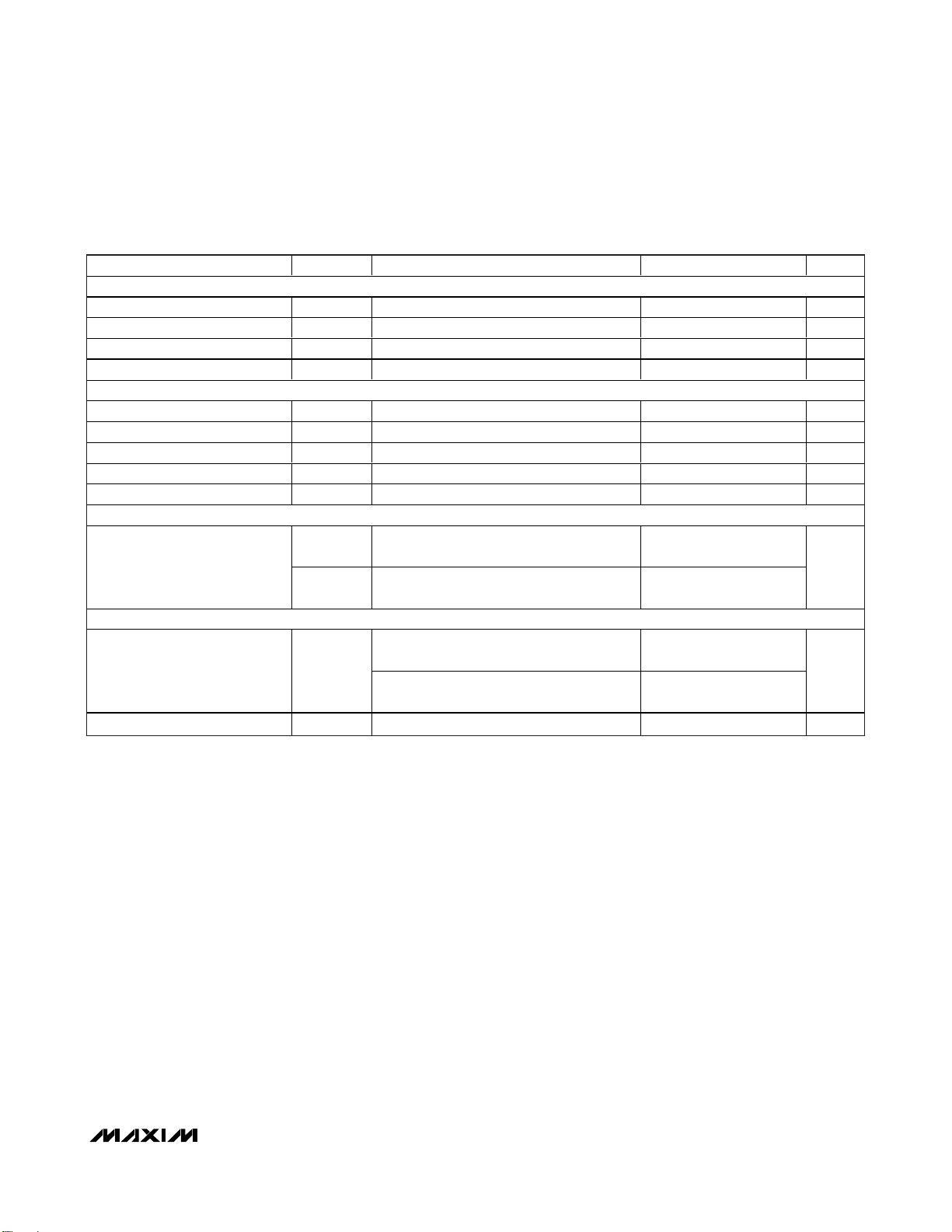
The MAX4929E has two enable inputs. The enable
function allows the device to operate in normal mode or
go into a high-Z state. It is possible to control two
MAX4929Es with a single control bit, creating a 4:1
equivalent switch using a minimum of external components (see Figure 6).
Supply or signals sequencing are not required for the
MAX4929E. Supply voltages V+, VL, and CLP can be
applied in any order. Signals can be applied in any
order as well.
Analog Switch
The MAX4929E features a voltage clamp function for the
two 2:1 switch. Inputs to SCL_/SDA_ are V+ level compatible. Maximum output voltages of SCLO/SDAO are
clamped to CLP. For optimum performance connect the
EDID EPROM supply voltage to CLP (see Figure 6). For
proper operation of the voltage clamp, connect
SCLO/SDAO to CLP through the pullup resistors. For
maximum output range, connect CLP to V+. The output of
the switch is connected to the EDID EPROM, voltages
from 3V to 5.5V are expected.
Logic Inputs
VL is the supply to input logic HIZ_, SEL, and HPD.
Connect VL to the same supply as the system MCU for
compatibility.
V+ is the supply to the input logic of the HPIR1 and
HPIR2 inputs.
Functional Diagram
SDA1
SDA2
SCL1
SCL2
HPIR1
HPIR2
HPDO1
HPDO2
HPD LOGIC
(V+)
MAX4929E
HPD LOGIC
(VL)
SDAO
SCLO
SEL
HPD
HPIRO
HIZ1
HIZ2
EXESD
GNDV+ CLP VL
Page 8

MAX4929E
HDMI 2:1 Low-Frequency Translating Switch
8 _______________________________________________________________________________________
Logic Outputs
The HPDO_ signals are 5V TTL-compatible, per HDMI/
DVI specifications. HPIRO is VL compatible.
ESD Protection
As with all Maxim devices, ESD-protection structures
are incorporated on all pins to protect against ESD
encountered during handling and assembly.
Additionally, the MAX4929E is protected to ±6kV (HBM)
on SCL1, SCL2, SDA1, SDA2, HPDO1, HPDO2, HPIR1,
and HPIR2 by the HBM.
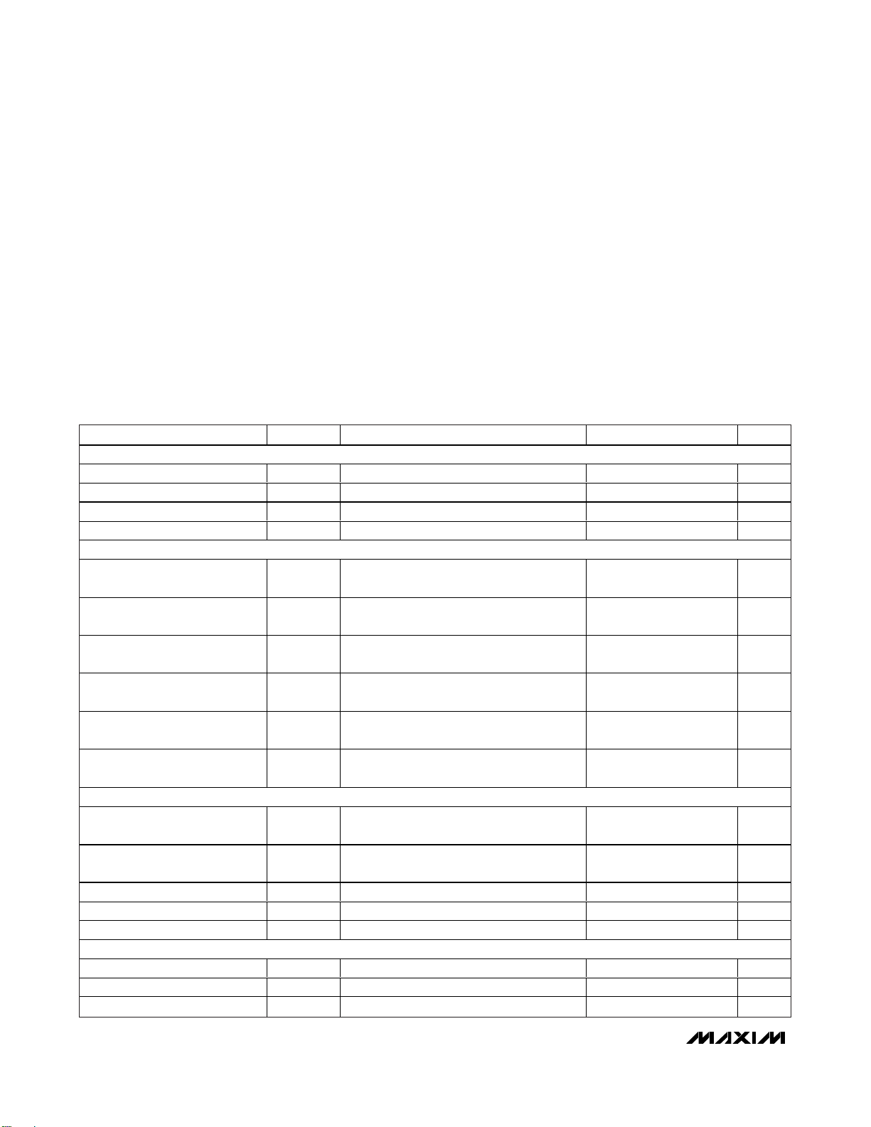
Human Body Model
Several ESD testing standards exist for measuring the
robustness against ESD events. The ESD protection of
the MAX4929E is characterized with the HBM method.
Figure 4 shows the model used to simulate an ESD event
resulting from contact with the human body. The model
consists of a 100pF storage capacitor that is charged to a
high voltage, then discharged through a 1.5kΩ resistor.
Figure 5 shows the current waveform when the storage
capacitor is discharged into a lower impedance.
ESD Test Conditions
ESD performance depends on a variety of conditions.
Contact Maxim for a reliability report documenting test
setup, methodology, and results.
Figure 4. Human Body ESD Test Model
Table 1. Inputs Selection for 2:1 Mux
Truth Table
Table 2. HPD Output Channel Selection
Table 3. HPIRO Output Channel Selection
Table 4. Mode of Operation
INPUTS
SEL HIZ1 HIZ2
0 0 1 SDAO to SDA1, SCLO to SCL1
0 1 0 SDAO to SDA1, SCLO to SCL1
1 0 1 SDAO to SDA2, SCLO to SCL2
1 1 0 SDAO to SDA2, SCLO to SCL2
X 0 0 High Impedance
X 1 1 High Impedance
SWITCH CONNECTIONS
INPUTS OUTPUTS
SEL HPD HIZ1 HIZ2 HPDO1 HPDO2
X0
01
11
XX11
XX00
0
1
0
1
0
1
1
0
1
0
1
0
00
10
01
High
Impedance
High
Impedance
High
Impedance
High
Impedance
INPUTS OUTPUTS
HIZ1 HIZ2 MODE OF OPERATION
00
0 1 Normal Operation
1 0 Normal Operation
11
HIGH-
VOLTAGE
DC
SOURCE
High-Impedance: SDAO, SDA1, SDA2,
SCLO, SCL1, SCL2, HPDO1, HPDO2, HPIRO
High-Impedance: SDAO, SDA1, SDA2,
SCLO, SCL1, SCL2, HPDO1, HPDO2, HPIRO
R
C
1MΩ
CHARGE-CURRENT-
LIMIT RESISTOR
C
100pF
s
R
D
1500Ω
DISCHARGE
RESISTANCE
STORAGE
CAPACITOR
DEVICE
UNDER
TEST
INPUTS OUTPUT
SEL HPIR1 HPIR2 HIZ1 HIZ2 HPIRO
X00
X11
00X
01X
1X0
1X1
XXX0 0
XXX1 1
0
1
0
1
0
1
0
1
0
1
0
1
1
0
1
0
1
0
1
0
1
0
1
0
0
1
0
1
0
1
High
Impedance
High
Impedance
Page 9

MAX4929E
HDMI 2:1 Low-Frequency Translating Switch
_______________________________________________________________________________________ 9
Applications Information
Power-Supply Bypassing and Sequencing
There is no power-supply sequencing required. Power
can be applied to V+, CLP, or VL in any order. Bypass
V+, VL, and CLP to GND using 0.1µF or larger ceramic
capacitors as close to the device as possible.
Hot Plug
The MAX4929E is designed for HDMI/DVI switching.
The MAX4929E permits hot-plugging to any inputs/
outputs regardless of the power status of the device.
A plug can be inserted, and thus connected to the
MAX4929E whether the device is powered up or not.
Therefore, sequencing of power supplies is not
required; V+, CLP, and VL can be applied in any order.
Configure Two Devices to Form 4:1 Switch
Two MAX4929Es can be connected together to form a
4:1 switch (see Figure 6).
Exposed Paddle
The MAX4929EETP+ provides an EP to improve thermal
performance in the TQFN package. Connect the EP to
GND or leave EP unconnected.
Figure 6. Two MAX4929Es Connected to Form a 4:1 Translating Switch
Figure 5. HBM Discharge Current Waveform
PEAK-TO-PEAK RINGING
I
r
(NOT DRAWN TO SCALE)
AMPERES
IP 100%
90%
36.8%
10%
0
0
t
RL
TIME
t
DL
CURRENT WAVEFORM
V
MCU
HPIR1, HPDO1,
SCL1, SDA1
HPIR2, HPDO2,
SCL2, SDA2
+5V
MAX4929E
V+
VL
HIZ1
HIZ2
GND
CHIP
SELECT
HDMI1
HDMI2
+3.3V TO +5V
EDID
EPROM
+2V TO +3.3V
MCU
CLP
EXESD
SCLO
SDAO
HPIRO
HPD
SEL
0.1μF
2kΩ
R
R
P
2kΩ
P
HDMI3
HDMI4
HPIR1, HPDO1,
SCL1, SDA1
HPIR2, HPDO2,
SCL2, SDA2
+5V
V
MCU
MAX4929E
V+
VL
HIZ1
HIZ2
GND
EXESD
CLP
SCLO
SDAO
HPIRO
HPD
SEL
0.1μF
Page 10

MAX4929E
HDMI 2:1 Low-Frequency Translating Switch
10 ______________________________________________________________________________________
Chip Information
PROCESS: BiCMOS
Pin Configurations (continued)
TOP VIEW
HPDO2
1
HPIR2
2
SDA2
3
4
SCL2
HPDO1
HPIR1
SDA1
SCL1
CLP
5
6
7
8
9
V+
10
MAX4929E
QSOP
20
EXESD
19
GND
18
HIZ1
17
HIZ2
16
HPD
HPIRO
15
14
SDAO
13
SCLO
12
SEL
11
VL
Page 11

MAX4929E
HDMI 2:1 Low-Frequency Translating Switch
______________________________________________________________________________________ 11
Package Information
(The package drawing(s) in this data sheet may not reflect the most current specifications. For the latest package outline information
go to www.maxim-ic.com/packages
.)
24L QFN THIN.EPS
Page 12

MAX4929E
HDMI 2:1 Low-Frequency Translating Switch
12 ______________________________________________________________________________________
Package Information (continued)
(The package drawing(s) in this data sheet may not reflect the most current specifications. For the latest package outline information
go to www.maxim-ic.com/packages
.)
Page 13

MAX4929E
HDMI 2:1 Low-Frequency Translating Switch
Maxim cannot assume responsibility for use of any circuitry other than circuitry entirely embodied in a Maxim product. No circuit patent licenses are
implied. Maxim reserves the right to change the circuitry and specifications without notice at any time.
Maxim Integrated Products, 120 San Gabriel Drive, Sunnyvale, CA 94086 408-737-7600 ____________________
13
© 2007 Maxim Integrated Products is a registered trademark of Maxim Integrated Products, Inc.
Package Information (continued)
(The package drawing(s) in this data sheet may not reflect the most current specifications. For the latest package outline information
go to www.maxim-ic.com/packages
.)
QSOP.EPS
 Loading...