

Page 1
General Description
The MAX4928A/MAX4928B high-speed passive switches route PCI Express
®
(PCIe) data and/or DisplayPort™
signals between two possible destinations in desktop or
laptop PCs. The MAX4928A is intended to be used with
the ATX form factor desktop PCs, while the MAX4928B
is expected to be used in the BTX form factor.
The MAX4928A/MAX4928B are hex double-pole/double-throw (6 x DPDT) switches. The MAX4928A/
MAX4928B feature a single digital control input (SEL) to
switch signal paths and a latch input (LE) that holds the
switches in a given state.
The MAX4928A/MAX4928B are fully specified to operate from a single +3.3V (typ) power supply. The
MAX4928A/MAX4928B are available in an industry
standard 5mm x 11mm, 56-pin TQFN package. Both
devices operate over the -40°C to +85°C extended
temperature range.
Applications
Desktop PCs
Notebook PCs
Features
♦ Single +3.3V Power Supply Voltage
♦ Supports PCIe Gen I, Gen II, and DisplayPort
Data Rates > 5Gbps
♦ Excellent Return Loss > 12dB at 2.5GHz
♦ Six Bidirectional Pairs of Switches
All Switching in One Device
♦ Low 850µA (max) Supply Current
♦ Small 5mm x 11mm, 56-Pin TQFN Package
♦ Industry-Standard Pinouts
MAX4928A/MAX4928B
DisplayPort/PCIe Passive Switches
________________________________________________________________
Maxim Integrated Products
1
19-4030; Rev 1; 8/08
For pricing, delivery, and ordering information, please contact Maxim Direct at 1-888-629-4642,
or visit Maxim’s website at www.maxim-ic.com.
Typical Operating Circuit appears at end of data sheet.
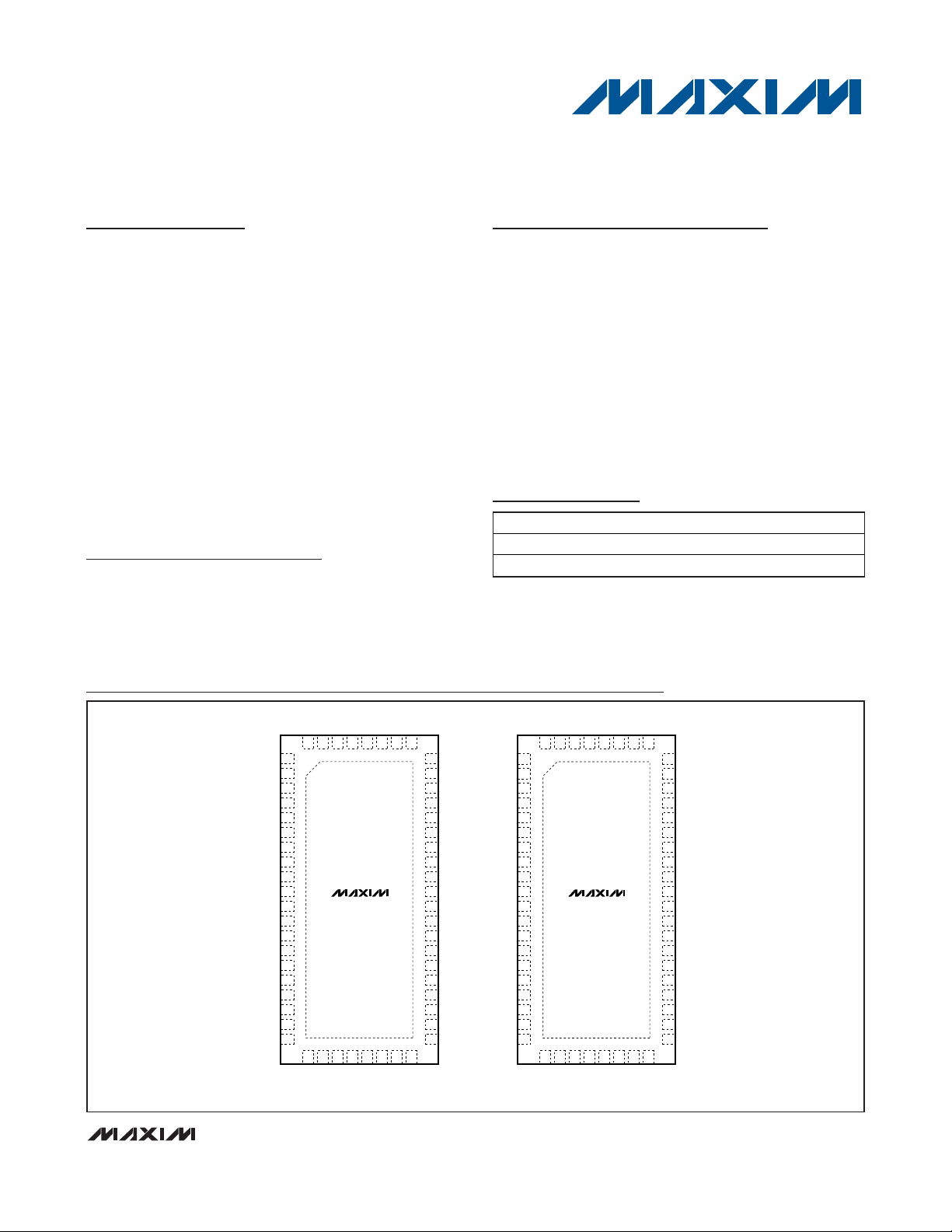
MAX4928A
21 22 23 24 25 26 27 28
V
DD
*EP
GND
TX0+
TX0-
TX1+
TX1-
V
DD
GND
GND
V
DD
HPD2
HPD1
AUX-
AUX+
V
DD
GND
48
47
46
45
44
43
54 5356 55 52 51 50 49
1
+
2
3
4
5
6
7
8
9
10
11
12
13
14
15
16
17
18
19
20
42
41
40
39
38
37
36
35
34
33
32
31
30
29
OUT+
OUT-
X+
GND
IN3-
IN3+
SEL
LE
GND
V
DD
GND
X-
IN2-
IN2+
V
DD
IN1-
IN1+
IN0-
IN0+
GND
D3+
D3-
GND
D2-
D2+
D1-
RX1+
RX1-
GND
RX0-
RX0+
V
DD
D1+
D0-
D0+
TX3-
TX3+
TX2-
TX2+
GND
*CONNECT EXPOSED PADDLE TO GND.
TQFN
TOP VIEW
MAX4928B
21 22 23 24 25 26 27 28
V
DD
*EP
GND
D0+
D0-
D1+
D1-
V
DD
GND
GND
V
DD
RX1-
RX1+
RX0-
RX0+
V
DD
GND
48
47
46
45
44
43
54 5356 55 52 51 50 49
1
+
2
3
4
5
6
7
8
9
10
11
12
13
14
15
16
17
18
19
20
42
41
40
39
38
37
36
35
34
33
32
31
30
29
IN3+
IN3-
OUT+
GND
IN2-
IN2+
X+
X-
GND
V
DD
GND
OUT-
IN1-
IN1+
V
DD
IN0-
IN0+
LE
SEL
GND
TX3+
TX3-
GND
TX2-
TX2+
TX1-
HPD1
HPD2
GND
AUX-
AUX+
V
DD
TX1+
TX0-
TX0+
D3-
D3+
D2-
D2+
GND
TQFN
Pin Configurations
PCI Express is a registered trademark of PCI-SIG.
DisplayPort is a trademark of Video Electronics Standards
Association (VESA).
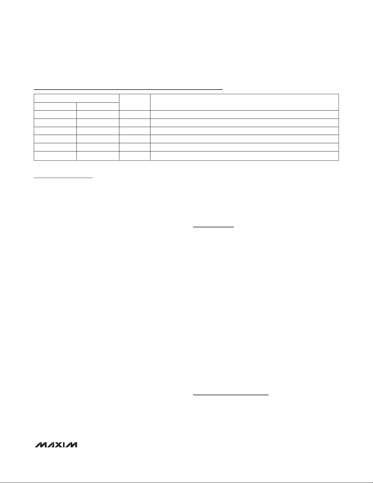
PART TEMP RANGE PIN-PACKAGE
MAX4928AETN+
-40°C to +85°F 56 TQFN-EP
MAX4928BETN+
-40°C to +85°F 56 TQFN-EP
Ordering Information
+
Denotes a lead-free package/RoHS-Compliant package.
EP = Exposed paddle.
Page 2
MAX4928A/MAX4928B
DisplayPort/PCIe Passive Switches
2 _______________________________________________________________________________________
ELECTRICAL CHARACTERISTICS
(VDD= +3.3V ±10%, TA=T
MIN
to T
MAX
, unless otherwise noted. Typical values are at VDD= +3.3V, TA= +25°C, unless otherwise
noted.) (Note 3)
Stresses beyond those listed under “Absolute Maximum Ratings” may cause permanent damage to the device. These are stress ratings only, and functional
operation of the device at these or any other conditions beyond those indicated in the operational sections of the specifications is not implied. Exposure to
absolute maximum rating conditions for extended periods may affect device reliability.
PARAMETER SYMBOL CONDITIONS
ANALOG SWITCH
Analog Signal Range
IN_, X_, OUT_,
D_, TX_, HPD_,
RX_, AUX_
(VDD -
V
Voltage Between IN and D/TX, X
and HPD/RX1, and OUT and
AUX/RX0
|V
IN_
- V
TX_
|,
|V
IN_
- VD_|,
|V
X_
- V
HPD_
|,
|V
OUT_
-
V
AUX_
|,
01.8V
On-Resistance R
ON
I
IN_
= IX_ = I
OUT_
= 15mA, VD_, V
TX_
,
V
HPD_
, V
AUX_
, or V
RX_
= 0V, +1.2V
8 Ω
On-Resistance Match
Between Pairs of Same Channel
ΔR
ON
V
D D
= + 3.0V , I
I N _
= I
X _
= I
OU T _
= 15m A,
V
D _, V T X _
, V
H P D _
, V
A U X _
, or V
R X _
= 0V
( N otes 4, 5)
0.1 2
On-Resistance Match
Between Channels
ΔR
ON
V
D D
= + 3.0V , I
I N _
= I
X _
= I
OU T _
= 15m A,
V
D _, V T X _
, V
H P D _
, V
A U X _
, or V
R X _
= 0V
( N otes 4, 5)
1.5 4
Ω
On-Resistance Flatness R
FLAT(ON)
V
D D
= + 3.0V , I
I N _
= I
X _
= I
OU T _
= 15m A,
V
D _, V T X _
, V
H P D _
, V
A U X _
, or V
R X _
= 0V ,
+ 1.2V ( N otes 5, 6)
0.3 1.5 Ω
ABSOLUTE MAXIMUM RATINGS
(All voltages referenced to GND, unless otherwise noted.)
V
DD
...........................................................................-0.3V to +4V
LE, SEL, IN_, X_, OUT_, D_, TX_, HPD_, RX_, AUX_
(Note 1) ...............................................-0.3V to + (V
DD
+ 0.3V)
|V
IN_
- V
TX_
|, |V
IN_
- VD_|, |VX_- V
HPD_
|, |VX_- V
RX1_
|,
|V
OUT_
- V
AUX_
|, |V
OUT_
- V
RX0_
| (Note 1)...................0 to +2V
Continuous Current (IN_ to D_/TX_, X_ to HPD_/RX1_,
OUT_ to AUX_/RX0_ .....................................................±70mA
Peak Current (IN_ to D_/TX_, X_ to HPD_/RX1_, OUT_ to
AUX_/RX0_) (pulsed at 1ms, 10% duty cycle) .............±70mA
Continuous Current (LE, SEL)...........................................±30mA
Peak Current (LE, SEL)
(pulsed at 1ms, 10% duty cycle)..................................±70mA
Continuous Power Dissipation (T
A
= +70°C) for Multilayer Board
56-Pin TQFN (derate 41.0mW/°C above +70°C) .......3279mW
Operating Temperature Range ...........................-40°C to +85°C
Junction Temperature......................................................+150°C
Storage Temperature Range .............................-65°C to +150°C
Package Junction-to-Ambient Thermal Resistance (θ
JA
)
(Note 2) .....................................................................24.4°C/W
Package Junction-to-Case Thermal Resistance (θ
JC
)
(Note 2) .......................................................................1.5°C/W
Lead Temperature (soldering) .........................................+300°C
Note 1: Signals on IN_, X_, OUT_, D_, TX_, HPD_, RX_, or AUX_, LE, SEL exceeding V
DD
or GND are clamped by internal diodes.
Limit forward-diode current to maximum current rating.
Note 2: Package thermal resistances were obtained using the method described in JEDEC specification JESD51-7, using a 4-layer
board. For detailed information on package thermal considerations, see www.maxim-ic.com/thermal-tutorial.
MIN TYP MAX UNITS
|VX_ - V
|V
OUT_
- V
RX1_
RX0_
-0.1
|,
|
1.8)
Page 3
MAX4928A/MAX4928B
DisplayPort/PCIe Passive Switches
_______________________________________________________________________________________ 3
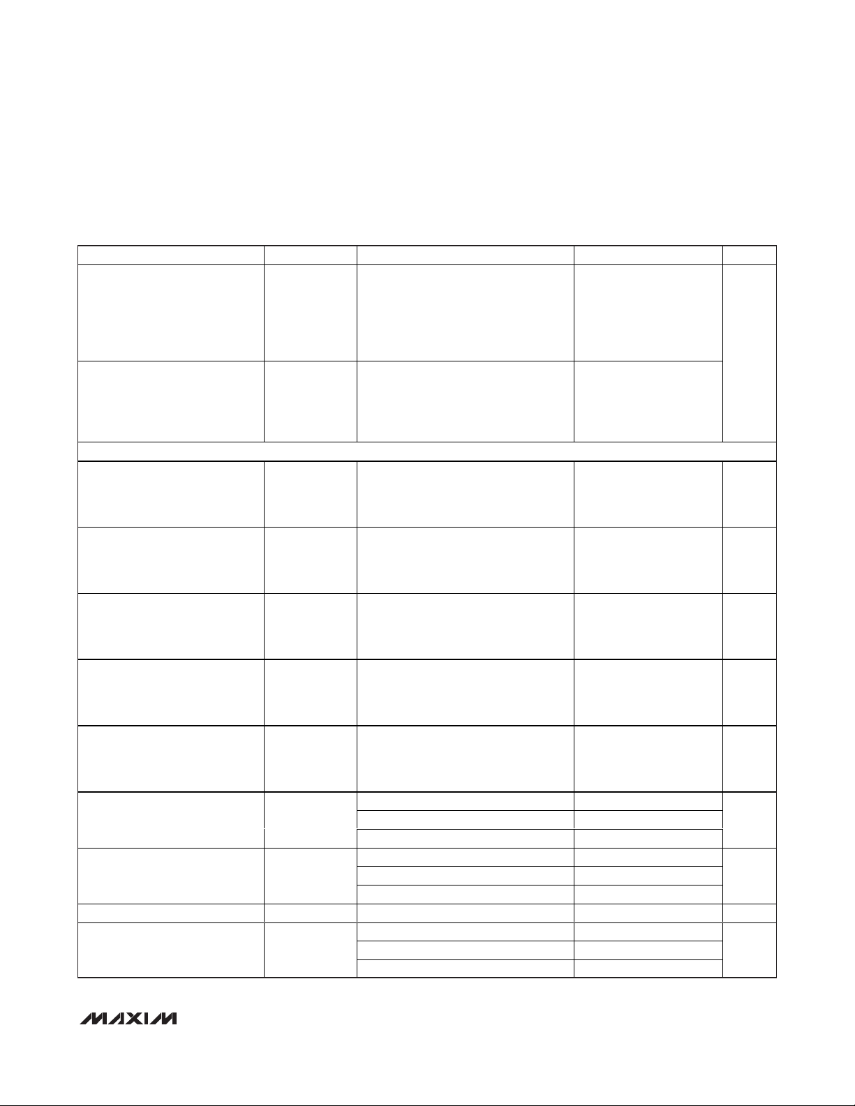
PARAMETER SYMBOL CONDITIONS
D_ or TX_/
HPD_ or RX1_/
AUX_ or RX0_ Off-Leakage
Current
I
D_ (OFF)
I
TX_ (OFF)
I
HPD_ (OFF)
I
RX1_ (OFF)
I
AUX_ (OFF)
I
RX0_ (OFF)
V
D D
= + 3.6V , V
I N _
= V
X _
= V
OU T _
= 0V ,
+ 1.2V ; V
D _
or V
T X _
, V
H P D _
or V
R X 1 _
,
V
A U X _
or V
R X 0 _
= + 1.2V , 0V
-1 +1
IN_/X_/OUT_ On-Leakage
Current
I
IN_ (ON)
I
X_ (ON)
I
OUT_ (ON)
V
D D
= + 3.6V , V
I N _
= V
X _
= V
OU T _
= 0V ,
+ 1.2V ; V
D _
or V
T X _
= V
I N _
or
unconnected , V
H P D _
or V
R X 1 _
= V
X _
or
unconnected , V
A U X _
or V
R X 0 _
= V
OU T _
or unconnected
-1 +1
µA
DIGITAL SIGNALS
SEL to Switch Turn-On Time t
ON_SEL
VD_ or V
TX_
= +1.0V, RL = 50Ω,
V
HPD_
or V
RX1_
= +1.0V, R
L
= 50Ω,
V
AUX_
or V
RX0_
= +1.0V, RL = 50Ω,
LE = V
DD
, CL = 100pf (Figure 1)
55 120 ns
SEL to Switch Turn-Off Time t
OFF_SEL
VD_ or V
TX_
= +1.0V, RL = 50Ω,
V
HPD_
or V
RX1_
= +1.0V, RL = 50Ω,
V
AUX_
or V
RX0_
= +1.0V, R
L
= 50Ω,
LE = V
DD
, CL = 100pf (Figure 1)
850ns
LE Setup Time
SEL to LE
t
SU
VD_ or V
TX_
= +1.0V, RL = 50Ω,
V
HPD_
or V
RX1_
= +1.0V, R
L
= 50Ω,
V
AUX_
or V
RX0_
= +1.0V, R
L
= 50Ω
(Figure 1)
2ns
LE Hold Time
SEL to LE
t
HOLD
VD_ or V
TX_
= +1.0V, RL = 50Ω,
V
HPD_
or V
RX1_
= +1.0V, RL = 50Ω,
V
AUX_
or V
RX0_
= +1.0V, RL = 50Ω,
(Figure 1)
2ns
LE Minimum Pulse-Width Low t
W
VD_ or V
TX_
= +1.0V, RL = 50Ω,
V
HPD_
or V
RX1_
= +1.0V, R
L
= 50Ω,
V
AUX_
or V
RX0_
= +1.0V, RL = 50Ω
(Figure 1)
40 ns
f = 2.5GHz
f = 5.0GHz
Differential Insertion Loss
(Figure 2)
S
DD21
f = 7.5GHz
dB
f = 2.5GHz -40
f = 5.0GHz -23Differential Crosstalk (Figure 2) S
DDCTK
f = 7.5GHz -28
dB
Differential Off-Isolation S
DD21_OFF
f = 3.0GHz -22 dB
f = 2.8GHz -21
f = 5.0GHz -8
Differential Return Loss (Figure 2)
S
DD11
f = 7.5GHz -7
dB
ELECTRICAL CHARACTERISTICS (continued)
(VDD= +3.3V ±10%, TA=T
MIN
to T
MAX
, unless otherwise noted. Typical values are at VDD= +3.3V, TA= +25°C, unless otherwise
noted.) (Note 3)
MIN TYP MAX UNITS
-1.5
-3.3
-4.9
Page 4
MAX4928A/MAX4928B
DisplayPort/PCIe Passive Switches
4 _______________________________________________________________________________________
PARAMETER SYMBOL CONDITIONS
Signal Data Rate BR RS = RL = 100Ω balanced 10
Differential -3dB Bandwidth DBW RS = RL = 100Ω balanced 5 GHz
LOGIC INPUT (LE, SEL)
Input Logic-High V
IH
1.4 V
Input Logic-Low V
IL
0.5 V
Input Logic Hysteresis V
HYST
100 mV
Input Leakage Current I
IN
VIN = 0 or V
DD
-1 +1 µA
POWER SUPPLY
Power Supply Range V
DD
3.0 3.6 V
VDD Supply Current I
DD
VIN = 0 or V
DD
µA
ELECTRICAL CHARACTERISTICS (continued)
(VDD= +3.3V ±10%, TA=T
MIN
to T
MAX
, unless otherwise noted. Typical values are at VDD= +3.3V, TA= +25°C, unless otherwise
noted.) (Note 3)
Note 3: All units are 100% production tested at T
A
= +85°C. Limits over the operating temperature range are guaranteed by design
and characterization and are not production tested.
Note 4: ΔR
ON
= R
ON (MAX)
- R
ON (MIN)
.
Note 5: Guaranteed by design. Not production tested.
Note 6: Flatness is defined as the difference between the maximum and minimum value of on-resistance as measured over the
specified analog signal range.
MIN TYP MAX UNITS
Gbps
850
Page 5

MAX4928A/MAX4928B
DisplayPort/PCIe Passive Switches
_______________________________________________________________________________________ 5
5.0
6.0
5.5
7.0
6.5
8.0
7.5
8.5
9.5
9.0
10.0
-0.1 0.3 0.50.1 0.7 0.9 1.1 1.3 1.5
ON-RESISTANCE vs. V
IN_
, VX_, V
OUT_
MAX4928A/B toc01
V
IN_
, VX_, V
OUT_
(V)
ON-RESISTANCE (Ω)
V
DD
= 3.3V
5.0
6.0
5.5
7.0
6.5
8.0
7.5
8.5
9.5
9.0
10.0
-0.1 0.3 0.50.1 0.7 0.9 1.1 1.3 1.5
ON-RESISTANCE vs. V
IN_
, VX_, V
OUT_
MAX4928A/B toc02
V
IN_
, VX_, V
OUT_
(V)
ON-RESISTANCE (Ω)
TA = +85°C
TA = +25°C
TA = -40°C
VDD = 3.3V
0
300
200
100
400
500
600
700
800
900
1000
-40 10-15 356085
SUPPLY CURRENT vs. TEMPERATURE
MAX4928A/B toc03
TEMPERATURE (°C)
SUPPLY CURRENT (μA)
V
DD
= 3.3V
0.5
0. 7
1.1
0.9
1.3
1.5
3.0 3.23.1 3.3 3.4 3.5 3.6
LOGIC THRESHOLD vs. SUPPLY VOLTAGE
SUPPLY VOLTAGE (V)
LOGIC THRESHOLD (V)
VDD = 3.3V
MAX4928A/B toc04
V
IH
V
IL
0
20
60
40
80
100
3.0 3.23.1 3.3 3.4 3.5 3.6
TURN-ON/OFF TIME vs. SUPPLY VOLTAGE
MAX4928A/B toc05
SUPPLY VOLTAGE (V)
TURN-ON/OFF TIME (ns)
t
ON_SEL
t
OFF_SEL
-10
10 10,0001,000100
DIFFERENTIAL INSERTION LOSS
0
-6
-8
-2
-4
MAX4928A/B toc06
FREQUENCY (MHz)
DIFFERENTIAL INSERTION LOSS (dB)
-80
10 10,0001,000100
DIFFERENTIAL OFF-ISOLATION
0
-60
-20
-40
MAX4928A/B toc07
FREQUENCY (MHz)
DIFFERENTIAL OFF-ISOLATION (dB)
-100
10 10,0001,000100
DIFFERENTIAL CROSSTALK
0
-600
-80
-20
-40
MAX4928A/B toc08
FREQUENCY (MHz)
DIFFERENTIAL CROSSTALK (dB)
-40
10 10,0001,000100
DIFFERENTIAL RETURN LOSS
0
-30
-10
-20
MAX4928A/B toc09
FREQUENCY (MHz)
DIFFERENTIAL RETURN LOSS (dB)
Typical Operating Characteristics
(TA = +25°C, unless otherwise noted.)
Page 6

MAX4928A/MAX4928B
DisplayPort/PCIe Passive Switches
6 _______________________________________________________________________________________
tr < 5ns
tf < 5ns
50%
V
IL
LOGIC
INPUT
SEL
V
N_
= VD_ OR V
TX_
, V
HPD_
OR V
RX1_
, V
AUX_
, OR V
RX0_
R
L
IN_, X_,
OR OUT_
GND LE
SEL
C
L
INCLUDES FIXTURE AND STRAY CAPACITANCE.
V
OUT
= V
N_ (
R
L
)
RL + R
ON
V
N_
V
IH
0V
0V
D_ OR TX_,
HPD_ OR
RX1_, AUX_
OR RX0_
0.9 x V
OUT
0.9 x V
OUT
0.9 x V
OUT
0.9 x V
OUT
t
ON_SEL
t
OFF_SEL
V
OUT
SWITCH
OUTPUT
TX_, RX1_,
OR RX0_
SWITCH
OUTPUT
D_, HPD_,
OR AUX
LOGIC
INPUT
SEL
LOGIC
INPUT
LE
V
DD
C
L
+3.3V
V
OUT
MAX4928A/MAX4928B
LOGIC
INPUT
LE
50% 50%
50% 50%
LOGIC
INPUT
LE
LOGIC
INPUT
SEL
V
IL
V
IH
V
IL
V
IH
t
W
t
SU
t
HOLD
t
ON_SEL
t
OFF_SEL
Test Circuits/Timing Diagrams
Figure 1. Switching Time
Page 7

MAX4928A/MAX4928B
DisplayPort/PCIe Passive Switches
_______________________________________________________________________________________ 7
IN_+
X_+
OUT_+
IN_-
X_-
OUT_-
D_+
D_-
V
DD
+3.3V
TX_+
RX1_+
RX0_+
TX_RX1_RX0_-
SELV
DD
GND
DIFFERENTIAL INSERTION-LOSS/DIFFERENTIAL RETURN LOSS
PORT 1
PORT 2
PORT 3
PORT 4
NETWORK
ANALYZER
0.1μF
DIFFERENTIAL INSERTION-LOSS = 20log
V
IN+
V
IN-
V
OUT+
V
OUT-
HPD_+
HPD_-
AUX_+
AUX_-
LE
0V
V
IN+
- V
IN-
V
OUT+
- V
OUT-
( )
MAX4928A
MAX4928B
IN_+
X_+
OUT_+
IN_-
X_-
OUT_-
D_+
D_-
V
DD
+3.3V
TX_+
RX1_+
RX0_+
TX_RX1_RX0_-
SELV
DD
GND
DIFFERENTIAL OFF-ISOLATION
PORT 1
PORT 2
PORT 3
PORT 4
NETWORK
ANALYZER
0.1μF
DIFFERENTIAL OFF-ISOLATION = 20log
V
IN+
V
IN-
V
OUT+
V
OUT-
HPD_+
HPD_-
AUX_+
AUX_-
LE
0V
V
IN+
- V
IN-
V
OUT+
- V
OUT-
( )
MAX4928A
MAX4928B
IN_+
X_+
OUT_+
IN_-
X_-
OUT_-
D_+/D_-
HPD_+/HPD_-
V
DD
+3.3V
IN_+
X_+
OUT_+
IN_-
X_-
OUT_-
SEL
0V OR V
DD
GND
DIFFERENTIAL CROSSTALK
PORT 1
PORT 2
PORT 3
PORT 4
NETWORK
ANALYZER
50Ω
50Ω
50Ω
50Ω
0.1μF
DIFFERENTIAL CROSSTALK = 20log
V
IN+
V
IN-
V
OUT+
V
OUT-
AUX_+/AUX_-
TX_+/TX_-
RX1_+/RX1_-
HP0_+/HP0_-
LE
0V
V
IN+
- V
IN-
V
OUT+
- V
OUT-
( )
MAX4928A
MAX4928B
50Ω
50Ω
50Ω
50Ω
50Ω
50Ω
50Ω
50Ω
50Ω
50Ω
50Ω
50Ω
50Ω
50Ω
50Ω
50Ω
50Ω
50Ω
50Ω
50Ω
50Ω
50Ω
50Ω
50Ω
50Ω
50Ω
MEASUREMENTS ARE STANDARDIZED AGAINST SHORTS AT IC TERMINALS.
DIFFERENTIAL OFF-ISOLATION IS MEASURED BETWEEN IN_ AND “OFF” D_ OR TX_, X_ AND “OFF” HPD_ OR RX1_, OUT_ AND “OFF” AUX_ OR RX0_ TERMINAL ON EACH SWITCH.
DIFFERENTIAL ON-LOSS IS MEASURED BETWEEN IN_ AND “ON” D_ OR TX_, X_ AND “ON” HPD_ OR RX1_, OUT_ AND “ON” AUX_ OR RX0_ TERMINAL ON EACH SWITCH.
DIFFERENTIAL CROSSTALK IS MEASURED BETWEEN ANY TWO PAIRS.
Test Circuits/Timing Diagrams (continued)
Figure 2. Differential On-Loss, Differential Off-Isolation, and Differential Crosstalk
Page 8

MAX4928A/MAX4928B
DisplayPort/PCIe Passive Switches
8 _______________________________________________________________________________________
Pin Description
PIN
MAX4928A MAX4928B
NAME FUNCTION
1, 11, 16, 20, 21,
28, 29, 35, 48,
49, 56
1, 11, 16, 20, 21,
28, 29, 35, 48,
49, 56
GND Ground
2 4 IN0+ Analog Switch 1—Common Positive Terminal
3 5 IN0- Analog Switch 1—Common Negative Terminal
4 7 IN1+ Analog Switch 2—Common Positive Terminal
5 8 IN1- Analog Switch 2—Common Negative Terminal
6, 17, 22, 27, 34,
50, 55
6, 17, 22, 27, 34,
50, 55
V
DD
Positive Supply Voltage Input. Connect VDD to a +3.0V to +3.6V supply voltage.
Bypass V
DD
to GND with a 0.1µF ceramic capacitor placed as close as possible
to the device. See the Board Layout section.
7 9 IN2+ Analog Switch 3—Common Positive Terminal
8 10 IN2- Analog Switch 3—Common Negative Terminal
9 12 IN3+ Analog Switch 4—Common Positive Terminal
10 13 IN3- Analog Switch 4—Common Negative Terminal
12 14 OUT+ Analog Switch 5—Common Positive Terminal
13 15 OUT- Analog Switch 5—Common Negative Terminal
14 18 X+ Analog Switch 6—Common Positive Terminal
15 19 X- Analog Switch 6—Common Negative Terminal
18 2 SEL Control Signal Input
19 3 LE Latch Enable Input
23 30 HPD2 Analog Switch 6—Normally Open Negative Terminal
24 31 HPD1 Analog Switch 6—Normally Open Positive Terminal
25 32 AUX- Analog Switch 5—Normally Open Negative Terminal
26 33 AUX+ Analog Switch 5—Normally Open Positive Terminal
30 23 RX1- Analog Switch 6—Normally Closed Negative Terminal
31 24 RX1+ Analog Switch 6—Normally Closed Positive Terminal
32 25 RX0- Analog Switch 5—Normally Closed Negative Terminal
33 26 RX0+ Analog Switch 5—Normally Closed Positive Terminal
36 44 D3- Analog Switch 4—Normally Open Negative Terminal
37 45 D3+ Analog Switch 4—Normally Open Positive Terminal
38 46 D2- Analog Switch 3—Normally Open Negative Terminal
39 47 D2+ Analog Switch 3—Normally Open Positive Terminal
40 51 D1- Analog Switch 2—Normally Open Negative Terminal
41 52 D1+ Analog Switch 2—Normally Open Positive Terminal
42 53 D0- Analog Switch 1—Normally Open Negative Terminal
43 54 D0+ Analog Switch 1—Normally Open Positive Terminal
44 36 TX3- Analog Switch 4—Normally Closed Negative Terminal
45 37 TX3+ Analog Switch 4—Normally Closed Positive Terminal
46 38 TX2- Analog Switch 3—Normally Closed Negative Terminal
Page 9
MAX4928A/MAX4928B
DisplayPort/PCIe Passive Switches
_______________________________________________________________________________________ 9
Detailed Description
The MAX4928A/MAX4928B high-speed passive switches
route PCI Express (PCIe) data and/or DisplayPort signals
between two possible destinations. The MAX4928A/
MAX4928B are ideal for routing signals between a graphics memory controller hub (GMCH) and either a
DisplayPort or PCIe connector.
The MAX4928A/MAX4928B feature a single digital control input (SEL) to switch signal paths and a latch input
(LE) that holds the switches in a given state.
Digital Control Input (SEL)
The MAX4928A/MAX4928B provide a single digital control input (SEL) to select the signal path between the
IN_ and D_/TX_, X_ and HPD_/RX1_, and OUT_ and
AUX_/RX0_ channels. The truth tables for the
MAX4928A/MAX4928B are depicted in the
Functional
Diagrams/Truth Table
. Drive SEL rail-to-rail to minimize
power consumption.
Latch Control Input (LE)
The MAX4928A/MAX4928B provide a single digital control input (LE) to latch the signal paths between the IN_
and D_/TX_, X_ and HPD_/RX1_, and OUT_ and
AUX_/RX0_ channels. When LE is driven high, the
switches are held in their previous state, regardless of
the input signal to SEL. Drive LE rail-to-rail to minimize
power consumption.
Analog Signal Levels
The MAX4928A/MAX4928B accept standard PCIe signals to a maximum of (VDD- 1.8V). Signals on the IN_+
channels are routed to either the D_+ or TX_+ channels,
signals on the X+ channel are routed to either HPD1 or
RX1+ channels, and signals on the OUT+ channel are
routed to either AUX+ or RX0+ channels. Signals on the
IN_- channels are routed to either the D_- or TX_- channels, signals on the X- channel are routed to either HPD2
or RX1- channels, and signals on the OUT- channel are
routed to either AUX- or RX0- channels. The
MAX4928A/MAX4928B are bidirectional switches, allowing IN_, X_, OUT_, D_, TX_, HPD_, RX_, and AUX_ to be
used as either inputs or outputs.
Applications Information
DisplayPort/PCIe Switching
The MAX4928A/MAX4928B primary applications are
aimed to switch between a GMCH and either a
DisplayPort or PCIe connector. The MAX4928A/
MAX4928B contain n-channel switches to permit differential signals to be selected between a PCIe Gen II
socket or to a DisplayPort connector. Each device handles up to six pairs of signals. The DisplayPort signal is
an AC-coupled 8b/10b encoded differential signal
ranging up to 2.7 Gbps. The PCIe Gen I and Gen II signals are AC-coupled, 8b/10b encoded differential signals ranging up to 5.0Gbps.
Board Layout
High-speed switches require proper layout and design
procedures for optimum performance. Keep designcontrolled impedance PCB traces as short as possible
or follow impedance layouts per the PCIe specification.
Ensure that power-supply bypass capacitors are
placed as close as possible to the device. Multiple
bypass capacitors are recommended. Connect all
grounds and the exposed pad to large ground planes.
Chip Information
PROCESS: CMOS
Pin Description (continued)
PIN
MAX4928A MAX4928B
NAME FUNCTION
47 39 TX2+ Analog Switch 3—Normally Closed Positive Terminal
51 40 TX1- Analog Switch 2—Normally Closed Negative Terminal
52 41 TX1+ Analog Switch 2—Normally Closed Positive Terminal
53 42 TX0- Analog Switch 1—Normally Closed Negative Terminal
54 43 TX0+ Analog Switch 1—Normally Closed Positive Terminal
— — EP Exposed Pad. Connect EP to GND. Exposed pad internally connected to GND.
Page 10

MAX4928A/MAX4928B
DisplayPort/PCIe Passive Switches
10 ______________________________________________________________________________________
LE SEL
IN_ TO TX_,
X_ TO RX1_,
OUT_ TO RX0_
IN_ TO DO_,
X_ TO HPD_,
OUT_ TO AUX_
1X
NO CHANGE
NO CHANGE
00
ON
OFF
01
OFF
ON
X = DON'T CARE.
MAX4928A
MAX4928B
GND
D0+
D0-
IN0+
SEL
IN0-
TX0+
TX0-
D1+
D1-
IN1+
IN1-
TX1+
TX1-
D2+
D2-
IN2+
IN2-
TX2+
TX2-
D3+
D3-
IN3+
IN3-
TX3+
TX3-
HPD1
HPD2
X+
X-
RX1+
RX1-
AUX+
AUX-
OUT+
OUT-
RX0+
RX0-
CONTROL LATCH
LE
V
DD
Functional Diagram/Truth Table
Page 11

MAX4928A/MAX4928B
DisplayPort/PCIe Passive Switches
______________________________________________________________________________________ 11
V
DD
GND
D0+
D0-
IN0+
SEL
IN0-
D1+
D1-
D2+
D2-
IN1+
IN1-
D3+
D3-
HPD1
HPD2
IN2+
IN2-
AUX+
AUX-
TX0+
TX0-
IN3+
IN3-
TX1+
TX1-
TX2+
TX2-
X+
X-
TX3+
TX3-
RX1+
RX1-
OUT+
OUT-
RX0+
RX0-
LE
GRAPHICS AND
MEMORY
CONTROLLER HUB
PCIe GRAPHICS CONNECTOR
PCIe BUFF 1
PCIe BUFF 2
PCIe BUFF 3
PCIe BUFF 4
PCIe IN
AUX
CHANNEL SELECT
DP CONNECTOR
D0
D1
D2
D3
D4
D5
D6
D7
HPD
AUX
AUX
V
CC
N
1.5kΩ
100kΩ
MAX4928A
MAX4928B
V
CC
= 1V
SUPPLY VOLTAGE VCC = 1V
Typical Operating Circuit
Page 12

MAX4928A/MAX4928B
DisplayPort/PCIe Passive Switches
12 ______________________________________________________________________________________
PACKAGE TYPE PACKAGE CODE DOCUMENT NO.
56 TQFN-EP T56511-1
21-0187
Package Information
For the latest package outline information and land patterns, go to www.maxim-ic.com/packages.
Page 13

MAX4928A/MAX4928B
DisplayPort/PCIe Passive Switches
Maxim cannot assume responsibility for use of any circuitry other than circuitry entirely embodied in a Maxim product. No circuit patent licenses are
implied. Maxim reserves the right to change the circuitry and specifications without notice at any time.
Maxim Integrated Products, 120 San Gabriel Drive, Sunnyvale, CA 94086 408-737-7600 ____________________
13
© 2008 Maxim Integrated Products is a registered trademark of Maxim Integrated Products, Inc.
Revision History
REVISION
NUMBER
REVISION
DATE
DESCRIPTION
PAGES
CHANGED
0 2/08 Initial release —
1 8/08 Changed functional diagram and limits 1, 2, 11
 Loading...