

19-0410; Rev 3; 7/96
±15kV ESD-Protected, Slew-Rate-Limited,
Low-Power, RS-485/RS-422 Transceivers
_______________General Description
The MAX481E, MAX483E, MAX485E, MAX487E–MAX491E,
and MAX1487E are low-power transceivers for RS-485 and
RS-422 communications in harsh environments. Each driver
output and receiver input is protected against ±15kV electrostatic discharge (ESD) shocks, without latchup. These parts
contain one driver and one receiver. The MAX483E,
MAX487E, MAX488E, and MAX489E feature reduced slewrate drivers that minimize EMI and reduce reflections caused
by improperly terminated cables, thus allowing error-free
data transmission up to 250kbps. The driver slew rates of the
MAX481E, MAX485E, MAX490E, MAX491E, and MAX1487E
are not limited, allowing them to transmit up to 2.5Mbps.
These transceivers draw as little as 120µA supply current
when unloaded or when fully loaded with disabled drivers
(see
Selection Table
MAX483E, and MAX487E have a low-current shutdown
mode in which they consume only 0.5µA. All parts operate
from a single +5V supply.
Drivers are short-circuit current limited, and are protected
against excessive power dissipation by thermal shutdown
circuitry that places their outputs into a high-impedance
state. The receiver input has a fail-safe feature that guarantees a logic-high output if the input is open circuit.
The MAX487E and MAX1487E feature quarter-unit-load
receiver input impedance, allowing up to 128 transceivers
on the bus. The MAX488E–MAX491E are designed for fullduplex communications, while the MAX481E, MAX483E,
MAX485E, MAX487E, and MAX1487E are designed for halfduplex applications. For applications that are not ESD sensitive see the pin- and function-compatible MAX481,
MAX483, MAX485, MAX487–MAX491, and MAX1487.
). Additionally, the MAX481E,
________________________Applications
Low-Power RS-485 Transceivers
Low-Power RS-422 Transceivers
____________________________Features
♦ ESD Protection: ±15kV—Human Body Model
♦ Slew-Rate Limited for Error-Free Data
Transmission (MAX483E/487E/488E/489E)
♦ Low Quiescent Current:
120µA (MAX483E/487E/488E/489E)
230µA (MAX1487E)
300µA (MAX481E/485E/490E/491E)
♦ -7V to +12V Common-Mode Input Voltage Range
♦ Three-State Outputs
♦ 30ns Propagation Delays, 5ns Skew
(MAX481E/485E/490E/491E/1487E)
♦ Full-Duplex and Half-Duplex Versions Available
♦ Allows up to 128 Transceivers on the Bus
(MAX487E/MAX1487E)
♦ Current Limiting and Thermal Shutdown for
Driver Overload Protection
______________Ordering Information
PIN-PACKAGETEMP. RANGEPART
MAX481ECPA
Ordering Information continued on last page.
8 Plastic DIP0°C to +70°C
8 SO0°C to +70°CMAX481ECSA
8 Plastic DIP-40°C to +85°CMAX481EEPA
8 SO-40°C to +85°CMAX481EESA
Level Translators
Transceivers for EMI-Sensitive Applications
Industrial-Control Local Area Networks
______________________________________________________________Selection Table
PART
NUMBER
MAX481E
MAX483E
MAX485E
MAX487E
MAX488E
MAX489E
MAX490E
MAX491E
MAX1487E
HALF/FULL
DUPLEX
Half
Half
Half
Half
Full
Full
Full
Full
Half
DATA RATE
(Mbps)
2.5
0.25
2.5
0.25
0.25
0.25
2.5
2.5
2.5
SLEW-RATE
LIMITED
No
Yes
No
Yes
Yes
Yes
No
No
No
LOW-POWER
SHUTDOWN
Yes
Yes
No
Yes
No
No
No
No
No
RECEIVER/
DRIVER
ENABLE
Yes
Yes
Yes
Yes
No
Yes
No
Yes
Yes
QUIESCENT
CURRENT
(µA)
300
120
300
120
120
120
300
300
230
NUMBER OF
TRANSMITTERS
ON BUS
32
32
32
128
32
32
32
32
128
PIN
COUNT
8
8
8
8
8
14
8
14
8
MAX481E/MAX483E/MAX485E/MAX487E–MAX491E/MAX1487E
________________________________________________________________
Maxim Integrated Products
1
For free samples & the latest literature: http://www.maxim-ic.com, or phone 1-800-998-8800

±15kV ESD-Protected, Slew-Rate-Limited,
Low-Power, RS-485/RS-422 Transceivers
ABSOLUTE MAXIMUM RATINGS
Supply Voltage (VCC).............................................................12V
Control Input Voltage (–R—E–, DE)...................-0.5V to (V
Driver Input Voltage (DI).............................-0.5V to (V
Driver Output Voltage (Y, Z; A, B)..........................-8V to +12.5V
Receiver Input Voltage (A, B).................................-8V to +12.5V
Receiver Output Voltage (RO)....................-0.5V to (V
Continuous Power Dissipation (T
8-Pin Plastic DIP (derate 9.09mW/°C above +70°C) ....727mW
Stresses beyond those listed under “Absolute Maximum Ratings” may cause permanent damage to the device. These are stress ratings only, and functional
operation of the device at these or any other conditions beyond those indicated in the operational sections of the specifications is not implied. Exposure to
absolute maximum rating conditions for extended periods may affect device reliability.
= +70°C)
A
CC
CC
CC
+ 0.5V)
+ 0.5V)
+ 0.5V)
DC ELECTRICAL CHARACTERISTICS
(VCC= 5V ±5%, TA= T
PARAMETER SYMBOL MIN TYP MAX UNITS
Differential Driver Output (no load) V
Differential Driver Output
(with load)
Change in Magnitude of Driver
Differential Output Voltage for
Complementary Output States
Driver Common-Mode Output
Voltage
Change in Magnitude of Driver
Common-Mode Output Voltage
for Complementary Output States
Input High Voltage V
Input Low Voltage V
Input Current I
Input Current
(A, B)
Receiver Differential Threshold
Voltage
Receiver Input Hysteresis ∆V
Receiver Output High Voltage V
Receiver Output Low Voltage V
Three-State (high impedance)
Output Current at Receiver
Receiver Input Resistance R
MIN
to T
, unless otherwise noted.) (Notes 1, 2)
MAX
OD1
V
∆V
∆V
R = 50Ω (RS-422)
OD2
R = 27Ω (RS-485), Figure 8
R = 27Ω or 50Ω, Figure 8
OD
V
R = 27Ω or 50Ω, Figure 8
OC
R = 27Ω or 50Ω, Figure 8
OD
DE, DI, –R—E
IH
DE, DI, –R—E
IL
DE, DI, –R—E
IN1
DE = 0V;
VCC= 0V or 5.25V,
all devices except
I
IN2
MAX487E/MAX1487E
MAX487E/MAX1487E,
DE = 0V, VCC= 0V or 5.25V
-7V ≤ VCM≤ 12V
V
TH
VCM= 0V
TH
IO= -4mA, VID= 200mV
OH
IO = 4mA, VID= -200mV
OL
I
0.4V ≤ VO≤ 2.4V
OZR
-7V ≤ VCM≤ 12V, all devices except
MAX487E/MAX1487E
IN
-7V ≤ V
CM
–
–
–
≤ 12V, MAX487E/MAX1487E 48 kΩ
14-Pin Plastic DIP (derate 10.00mW/°C above +70°C)..800mW
8-Pin SO (derate 5.88mW/°C above +70°C).................471mW
14-Pin SO (derate 8.33mW/°C above +70°C)...............667mW
Operating Temperature Ranges
MAX4_ _C_ _/MAX1487EC_ A.............................0°C to +70°C
MAX4_ _E_ _/MAX1487EE_ A...........................-40°C to +85°C
Storage Temperature Range.............................-65°C to +160°C
Lead Temperature (soldering, 10sec).............................+300°C
CONDITIONS
2
1.5 5
0.2 V
0.2 V
2.0 V
0.8 V
±2 µA
VIN= 12V
VIN= -7V
VIN= 12V
VIN= -7V
-0.2 0.2 V
3.5
12 kΩ
1.0
-0.8
0.25
-0.2
70 mV
0.4
±1 µA
5 V
V
3 V
mA
mA
V
V
MAX481E/MAX483E/MAX485E/MAX487E–MAX491E/MAX1487E
2 _______________________________________________________________________________________
±15kV ESD-Protected, Slew-Rate-Limited,
Low-Power, RS-485/RS-422 Transceivers
DC ELECTRICAL CHARACTERISTICS (continued)
(VCC= 5V ±5%, TA= T
No-Load Supply Current
(Note 3)
Supply Current in Shutdown
Driver Short-Circuit Current,
VO= High
Driver Short-Circuit Current,
VO= Low
Receiver Short-Circuit Current
MIN
to T
, unless otherwise noted.) (Notes 1, 2)
MAX
MAX488E/MAX489E,
DE, DI, –R—E–= 0V or V
MAX490E/MAX491E,
DE, DI, –R—E–= 0V or V
MAX481E/MAX485E,
–R—E–
I
CC
SHDN
OSD1
OSD2
I
OSR
= 0V or V
MAX1487E,
–R—E–
= 0V or V
MAX483E/MAX487E,
–R—E–
= 0V or V
CC
CC
CC
CC
CONDITIONS UNITSMIN TYP MAXSYMBOLPARAMETER
CC
CC
DE = V
CC
120 250
300 500
500 900
300 500DE = 0V
DE = V
DE = 0V
DE = V
DE = 0V
CC
CC
MAX483E
MAX487E
CC
300 500
230 400
350 650
250 400
120 250
0.5 10I
7950V ≤ VO≤ V
SWITCHING CHARACTERISTICS—MAX481E/MAX485E, MAX490E/MAX491E, MAX1487E
(VCC= 5V ±5%, TA= T
PARAMETER SYMBOL MIN TYP MAX UNITS
Driver Input to Output
Driver Output Skew to Output
Driver Rise or Fall Time tR, t
Driver Enable to Output High t
Driver Enable to Output Low t
Driver Disable Time from Low t
Driver Disable Time from High
Receiver Input to Output t
| t
- t
PLH
| Differential
PHL
Receiver Skew
Receiver Enable to Output Low t
Time to Shutdown t
MIN
to T
, unless otherwise noted.) (Notes 1, 2)
MAX
t
Figures 10 and 12, R
PLH
CL1= CL2= 100pF
t
PHL
t
SKEW
Figures 10 and 12, R
Figures 10 and 12,
R
F
ZH
ZL
LZ
t
HZ
= 54Ω,
DIFF
CL1= CL2= 100pF
Figures 11 and 13, CL= 100pF, S2 closed
Figures 11 and 13, CL= 100pF, S1 closed
Figures 11 and 13, CL= 15pF, S1 closed
Figures 11 and 13, CL= 15pF, S2 closed
Figures 10 and 14,
, t
R
PLH
t
SKD
ZL
t
ZH
LZ
HZ
MAX
SHDN
PHL
= 54Ω,
DIFF
CL1= CL2= 100pF
Figures 10 and 14, R
CL1= CL2= 100pF
Figures 9 and 15, CRL= 15pF, S1 closed
Figures 9 and 15, CRL= 15pF, S2 closed
Figures 9 and 15, CRL= 15pF, S1 closed
Figures 9 and 15, CRL= 15pF, S2 closed
MAX481E (Note 5)
CONDITIONS
= 54Ω,
DIFF
= 54Ω, CL1= CL2= 100pF
DIFF
MAX481E, MAX485E, MAX1487E
MAX481E, MAX485E, MAX1487E
MAX490EC/E, MAX491EC/E
= 54Ω,
DIFF
10 40 60
10 40 60
510
32040
52025MAX490EC/E, MAX491EC/E
45 70
45 70 ns
45 70
45 70
20 60 200
20 60 150
5 ns
20 50
20 50
20 50
20 50
2.5
50 200 600
MAX481E/MAX483E/MAX485E/MAX487E–MAX491E/MAX1487E
µA
µAMAX481E/483E/487E, DE = 0V, –R—E–= V
mA35 250-7V ≤ VO≤12V (Note 4)I
mA35 250-7V ≤ VO≤12V (Note 4)I
mA
kV±15A, B, Y and Z pins, tested using Human Body ModelESD Protection
ns
ns
ns
ns
ns
ns
ns
ns
nsReceiver Enable to Output High
nsReceiver Disable Time from Low t
nsReceiver Disable Time from High t
MbpsMaximum Data Rate f
ns
_______________________________________________________________________________________ 3
±15kV ESD-Protected, Slew-Rate-Limited,
Low-Power, RS-485/RS-422 Transceivers
SWITCHING CHARACTERISTICS—MAX481E/MAX485E, MAX490E/MAX491E, MAX1487E
(VCC= 5V ±5%, TA= T
Driver Enable from Shutdown to
Output High (MAX481E)
Driver Enable from Shutdown to
Output Low (MAX481E)
Receiver Enable from Shutdown
to Output High (MAX481E)
Receiver Enable from Shutdown
to Output Low (MAX481E)
MIN
to T
, unless otherwise noted.) (Notes 1, 2)
MAX
ZH(SHDN)
ZL(SHDN)
ZH(SHDN)
t
ZL(SHDN)
SWITCHING CHARACTERISTICS—MAX483E, MAX487E/MAX488E/MAX489E
(VCC= 5V ±5%, TA= T
Driver Input to Output
Driver Output Skew to Output ns20 800
Driver Rise or Fall Time
Driver Enable to Output High
Driver Enable to Output Low
Driver Disable Time from Low
Driver Disable Time from High
Receiver Input to Output
I t
- t
PLH
Receiver Skew
Receiver Enable to Output Low
Receiver Enable to Output High
Receiver Disable Time from Low
Receiver Disable Time from High
Maximum Data Rate
Time to Shutdown
Driver Enable from Shutdown to
Output High
Driver Enable from Shutdown to
Output Low
Receiver Enable from Shutdown
to Output High
Receiver Enable from Shutdown
to Output Low
MAX481E/MAX483E/MAX485E/MAX487E–MAX491E/MAX1487E
I Differential
PHL
MIN
to T
, unless otherwise noted.) (Notes 1, 2)
MAX
t
PLH
t
PHL
t
SKEW
ZH
ZL
LZ
HZ
t
PLH
t
PHL
t
SKD
ZL
ZH
LZ
HZ
MAX
SHDN
t
ZH(SHDN)
t
ZL(SHDN)
t
ZH(SHDN)
t
ZL(SHDN)
(continued)
CONDITIONS
Figures 11 and 13, CL= 100pF, S2 closed
Figures 11 and 13, CL= 100pF, S1 closed
Figures 9 and 15, CL= 15pF, S2 closed,
A - B = 2V
Figures 9 and 15, CL= 15pF, S1 closed,
B - A = 2V
CONDITIONS
Figures 10 and 12, R
CL1= CL2= 100pF
Figures 10 and 12, R
CL1= CL2= 100pF
Figures 10 and 12, R
F
CL1= CL2= 100pF
Figures 11 and 13, CL= 100pF, S2 closed
Figures 11 and 13, CL= 100pF, S1 closed
Figures 11 and 13, CL= 15pF, S1 closed
Figures 11 and 13, CL= 15pF, S2 closed
Figures 10 and 14, R
CL1= CL2= 100pF
Figures 10 and 14, R
CL1= CL2= 100pF
Figures 9 and 15, CRL= 15pF, S1 closed
Figures 9 and 15, CRL= 15pF, S2 closed
Figures 9 and 15, CRL= 15pF, S1 closed
Figures 9 and 15, CRL= 15pF, S2 closed
t
, t
PLH
MAX483E/MAX487E, Figures 11 and 13,
CL= 100pF, S2 closed
MAX483E/MAX487E, Figures 11 and 13,
CL= 100pF, S1 closed
MAX483E/MAX487E, Figures 9 and 15,
CL= 15pF, S2 closed
MAX483E/MAX487E, Figures 9 and 15,
CL= 15pF, S1 closed
< 50% of data period
PHL
DIFF
DIFF
DIFF
DIFF
DIFF
= 54Ω,
= 54Ω,
= 54Ω,
= 54Ω,
= 54Ω,
225 1000
250 800 2000
250 800 2000
250 2000t
300 3000t
250 2000
250 2000
100
25 50t
UNITSMIN TYP MAXSYMBOLPARAMETER
ns45 100t
ns45 100t
ns225 1000t
ns
UNITSMIN TYP MAXSYMBOLPARAMETER
ns
ns250 2000tR, t
ns
ns250 2000t
ns300 3000t
ns
ns
ns
ns25 50t
ns25 50t
ns
ns25 50t
kbps250f
ns50 200 600MAX483E/MAX487E (Note 5) t
ns2000
ns2000
ns2500
ns2500
4 _______________________________________________________________________________________
±15kV ESD-Protected, Slew-Rate-Limited,
Low-Power, RS-485/RS-422 Transceivers
NOTES FOR ELECTRICAL/SWITCHING CHARACTERISTICS
Note 1: All currents into device pins are positive; all currents out of device pins are negative. All voltages are referenced to device
ground unless otherwise specified.
Note 2: All typical specifications are given for V
Note 3: Supply current specification is valid for loaded transmitters when DE = 0V.
Note 4: Applies to peak current. See
Typical Operating Characteristics.
= 5V and TA= +25°C.
CC
Note 5: The MAX481E/MAX483E/MAX487E are put into shutdown by bringing–R—E–high and DE low. If the inputs are in this state for
less than 50ns, the parts are guaranteed not to enter shutdown. If the inputs are in this state for at least 600ns, the parts are
guaranteed to have entered shutdown. See
Low-Power Shutdown Mode
section.
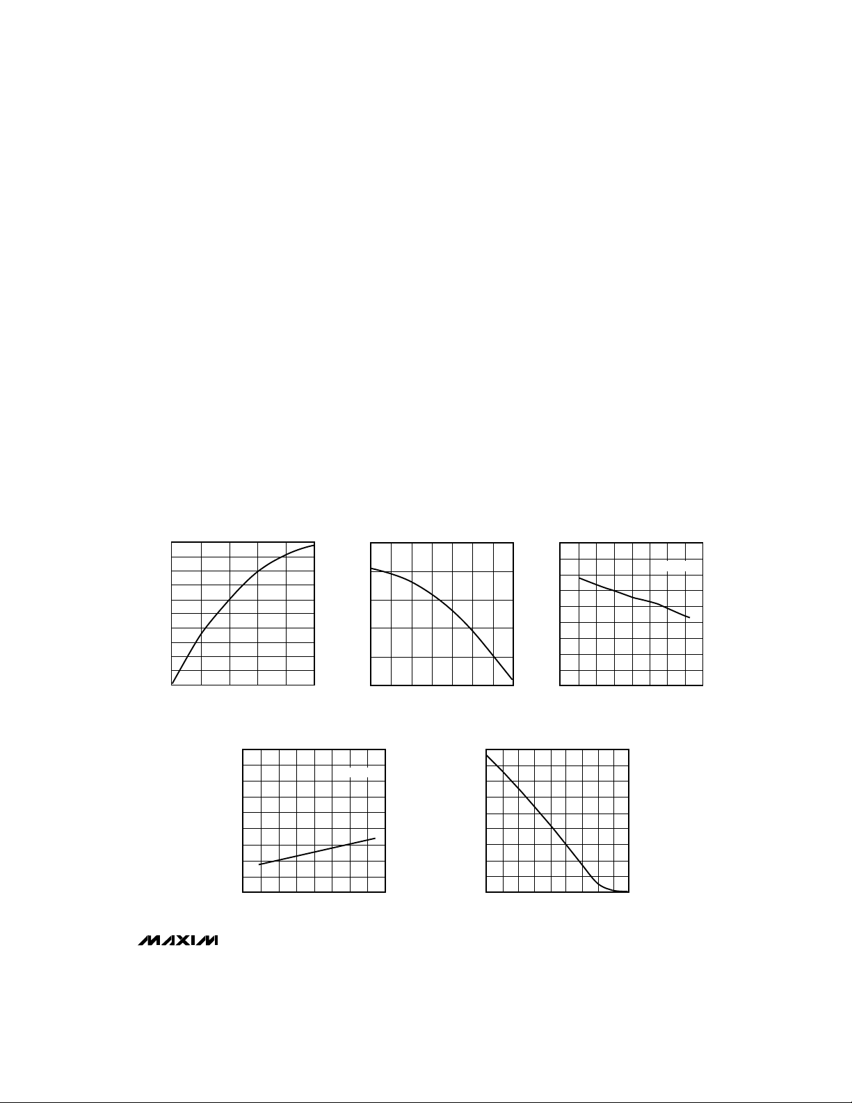
__________________________________________Typical Operating Characteristics
(VCC= 5V, TA = +25°C, unless otherwise noted.)
OUTPUT CURRENT vs.
RECEIVER OUTPUT LOW VOLTAGE
50
45
40
35
30
25
20
15
OUTPUT CURRENT (mA)
10
5
0
OUTPUT LOW VOLTAGE (V)
OUTPUT LOW VOLTAGE (V)
1.5 2.0 2.51.00.50
RECEIVER OUTPUT LOW VOLTAGE
0.9
0.8
0.7
0.6
0.5
0.4
0.3
0.2
0.1
0
-60 -20 60
vs. TEMPERATURE
20 100-40 40080
TEMPERATURE (°C)
-25
MAX481E-01
-20
-15
-10
OUTPUT CURRENT (mA)
-5
0
I
= 8mA
RO
OUTPUT CURRENT vs.
RECEIVER OUTPUT HIGH VOLTAGE
1.5 3.0
OUTPUT HIGH VOLTAGE (V)
MAX481E-04
OUTPUT CURRENT (mA)
4.8
4.6
MAX481E-02
4.4
4.2
4.0
3.8
3.6
OUTPUT HIGH VOLTAGE (V)
3.4
3.2
3.0
5.04.54.02.0 2.5 3.5
DRIVER OUTPUT CURRENT vs.
DIFFERENTIAL OUTPUT VOLTAGE
90
80
70
60
50
40
30
20
10
0
1.5 2.0 2.5 3.0 3.5 4.0 4.51.00.50
DIFFERENTIAL OUTPUT VOLTAGE (V)
RECEIVER OUTPUT HIGH VOLTAGE
vs. TEMPERATURE
I
-60 -20 60
20 100-40 40080
TEMPERATURE (°C)
MAX481E-05
RO
= 8mA
MAX481E/MAX483E/MAX485E/MAX487E–MAX491E/MAX1487E
MAX481E-03
_______________________________________________________________________________________
5

±15kV ESD-Protected, Slew-Rate-Limited,
Low-Power, RS-485/RS-422 Transceivers
____________________________Typical Operating Characteristics (continued)
(VCC= 5V, TA = +25°C, unless otherwise noted.)
DRIVER DIFFERENTIAL OUTPUT
VOLTAGE vs. TEMPERATURE
2.3
2.2
2.1
2.0
1.9
1.8
1.7
1.6
DIFFERENTIAL OUTPUT VOLTAGE (V)
1.5
-60 -20 60
MAX481E/MAX485E/MAX490E/MAX491E
SUPPLY CURRENT vs. TEMPERATURE
600
500
400
300
200
SUPPLY CURRENT (µA)
100
0
-60 -20 60
20 100-40 40080
TEMPERATURE (°C)
MAX481E/MAX485E; DE = VCC, RE = X
MAX485E; DE = 0, RE = X,
MAX481E; DE = RE = 0
MAX490E/MAX491E; DE = RE = X
MAX481E; DE = 0, RE = V
20 100-40 40080
TEMPERATURE (°C)
R = 54Ω
CC
140
MAX481E-06
120
100
80
60
40
OUTPUT CURRENT (mA)
20
0
600
MAX481E-09
500
400
300
200
SUPPLY CURRENT (µA)
100
0
-60 -20 60
OUTPUT CURRENT vs.
DRIVER OUTPUT LOW VOLTAGE
MAX481E-07
024681012
OUTPUT LOW VOLTAGE (V)
MAX483E/MAX487E–MAX489E
SUPPLY CURRENT vs. TEMPERATURE
MAX481E-10
MAX483E; DE = VCC, RE = X
MAX487E; DE = VCC, RE = X
MAX483E/MAX487E; DE = RE = 0,
MAX488E/MAX489E; DE = RE = X
MAX483E/MAX487E; DE = 0, RE = V
20 100-40 40080
TEMPERATURE (°C)
CC
OUTPUT CURRENT vs.
DRIVER OUTPUT HIGH VOLTAGE
-100
-90
-80
-70
-60
-50
-40
-30
OUTPUT CURRENT (mA)
-20
-10
0
-8 -2
OUTPUT HIGH VOLTAGE (V)
SUPPLY CURRENT vs. TEMPERATURE
600
500
400
300
200
SUPPLY CURRENT (µA)
100
0
-60 -20 60
MAX1487E
MAX1487E; DE = VCC, RE = X
MAX1487E; DE = 0V, RE = X
20 100-40 40080
TEMPERATURE (°C)
MAX481E-08
642-6 -4 0
MAX481E-11
MAX481E/MAX483E/MAX485E/MAX487E–MAX491E/MAX1487E
6 _______________________________________________________________________________________

±15kV ESD-Protected, Slew-Rate-Limited,
Low-Power, RS-485/RS-422 Transceivers
______________________________________________________________Pin Description
PIN
MAX481E/MAX483E/MAX485E/MAX487E–MAX491E/MAX1487E
MAX481E/MAX483E/MAX485E/MAX487E–MAX491E/MAX1487E
MAX481E/MAX483E
MAX485E/MAX487E
MAX1487E
1 2
2 —
3 —
4 3
5 4 Ground
— 5 Noninverting Driver Output
— 6 Inverting Driver Output
6 —
— 8 Noninverting Receiver Input
7 — Inverting Receiver Input and Inverting Driver Output
— 7 Inverting Receiver Input
8 1 Positive Supply: 4.75V ≤ VCC≤ 5.25V
— — No Connect—not internally connected
MAX488E
MAX490E
MAX489E
MAX491E
2
3
4
5
6, 7
9
10
—
12
—
11
14
1, 8, 13
NAME
RO
–R—E–
DE
DI
GND
Y
Z
A
A
B
B
V
CC
N.C.
Receiver Output: If A > B by 200mV, RO will be high;
If A < B by 200mV, RO will be low.
Receiver Output Enable. RO is enabled when–R—E–is
low; RO is high impedance when–R—E–is high.
Driver Output Enable. The driver outputs, Y and Z, are
enabled by bringing DE high. They are high impedance when DE is low. If the driver outputs are enabled,
the parts function as line drivers. While they are high
impedance, they function as line receivers if–R—E–is low.
Driver Input. A low on DI forces output Y low and output Z high. Similarly, a high on DI forces output Y high
and output Z low.
Noninverting Receiver Input and Noninverting Driver
Output
FUNCTION
_______________________________________________________________________________________ 7

±15kV ESD-Protected, Slew-Rate-Limited,
Low-Power, RS-485/RS-422 Transceivers
MAX481E
0.1µF
TOP VIEW
RO
2
RE
3
DE
4
D
DI
8
V
CC
7
B
6
A
5
GND
R
1
RO
RE
DE
R
1
2
3
4
D
DI
8
V
CC
B
7
Rt
6
A
5
GND
DIP/SO
NOTE: PIN LABELS Y AND Z ON TIMING, TEST, AND WAVEFORM DIAGRAMS REFER TO PINS A AND B WHEN DE IS HIGH.
TYPICAL OPERATING CIRCUIT SHOWN WITH DIP/SO PACKAGE.
Figure 1. MAX481E/MAX483E/MAX485E/MAX487E/MAX1487E Pin Configuration and Typical Operating Circuit
MAX483E
MAX485E
MAX487E
MAX1487E
B
Rt
A
DE
DI
D
R
RO
RE
TOP VIEW
V
GND
0.1µF
V
1
CC
Y
3
A
1
CC
RO
R
2
3
DI
4
D
8
B
7
6
Z
Y
5
DI
RO
DR
2
5
6
Z
8
A
R
7
B
MAX488E
MAX490E
Rt
Rt
V
CC
RO
DI
D
DIP/SO
4
GND
NOTE: TYPICAL OPERATING CIRCUIT SHOWN WITH DIP/SO PACKAGE.
GND
Figure 2. MAX488E/MAX490E Pin Configuration and Typical Operating Circuit
V
CC
TOP VIEW
N.C.
GND
GND
1
R
2
RO
3
RE
4
DE
5
DI
6
7
14
V
CC
13
N.C.
DI
A
12
B
11
10
Z
D
9
8
Y
N.C.
RO
1, 8, 13
NC
DIP/SO
MAX481E/MAX483E/MAX485E/MAX487E–MAX491E/MAX1487E
Figure 3. MAX489E/MAX491E Pin Configuration and Typical Operating Circuit
DE
5
D
2
RD
3 6, 7
RE
0.1µF
144
9
10
12
11
GND
MAX489E
MAX491E
Y
Z
A
Rt
B
VCCRE
Rt
R
GND DE
RO
DI
8 _______________________________________________________________________________________

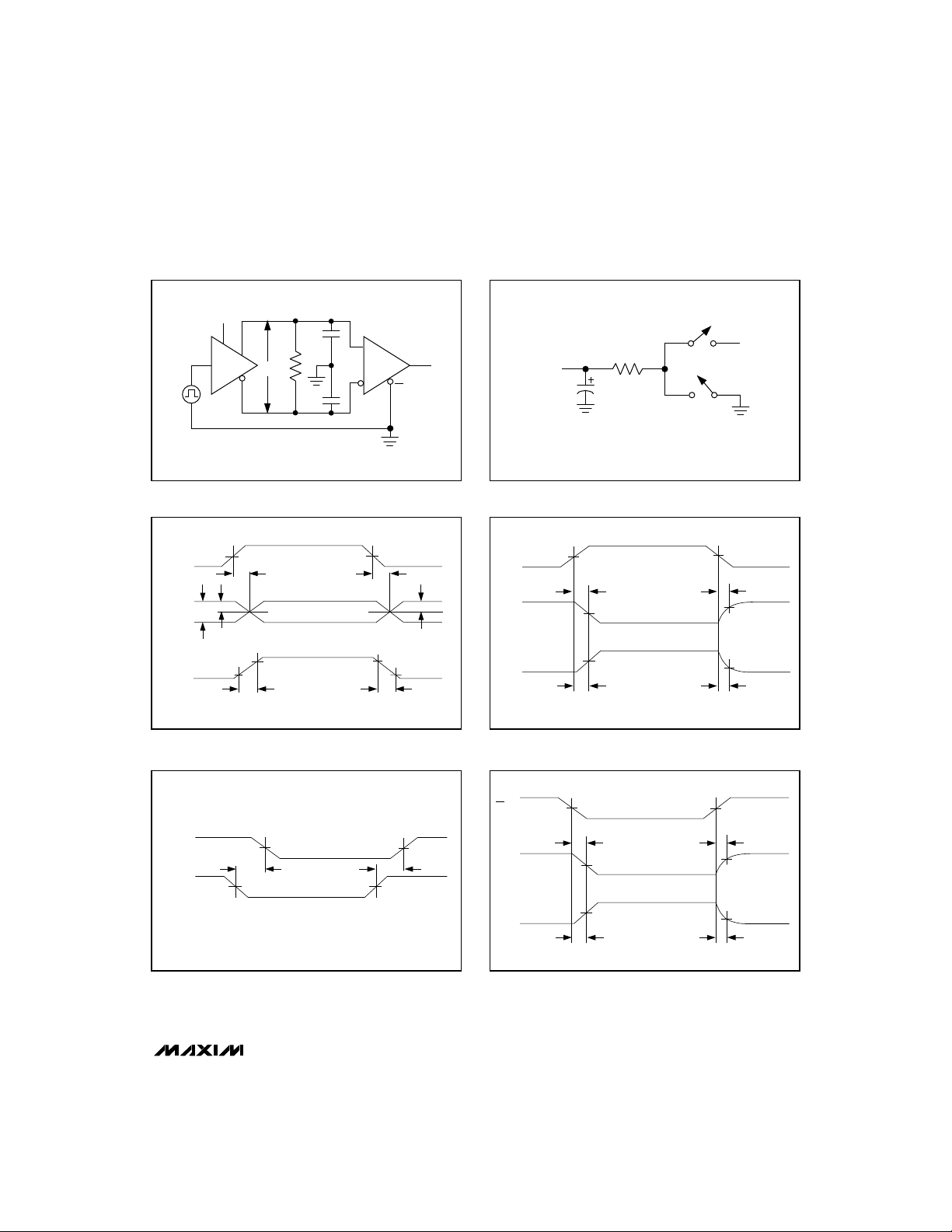
±15kV ESD-Protected, Slew-Rate-Limited,
Low-Power, RS-485/RS-422 Transceivers
__________Function Tables
(MAX481E/MAX483E/MAX485E/MAX487E/MAX1487E)
Table 1. Transmitting Table 2. Receiving
INPUTS OUTPUTS
RE
X
X
0
1
X = Don't care
High-Z = High impedance
Shutdown mode for MAX481E/MAX483E/MAX487E
*
DE DI Z Y
1
1
0
0
1
0
X
X
0
1
High-Z
High-Z
High-Z
High-Z
*
1
0
*
__________Applications Information
The MAX481E/MAX483E/MAX485E/MAX487E–MAX491E
and MAX1487E are low-power transceivers for RS-485
and RS-422 communications. These “E” versions of the
MAX481, MAX483, MAX485, MAX487–MAX491, and
MAX1487 provide extra protection against ESD. The
rugged MAX481E, MAX483E, MAX485E, MAX497E–
MAX491E, and MAX1487E are intended for harsh environments where high-speed communication is important.
These devices eliminate the need for transient suppressor diodes and the associated high capacitance loading.
The standard (non-“E”) MAX481, MAX483, MAX485,
MAX487–MAX491, and MAX1487 are recommended for
applications where cost is critical.
The MAX481E, MAX485E, MAX490E, MAX491E, and
MAX1487E can transmit and receive at data rates up to
2.5Mbps, while the MAX483E, MAX487E, MAX488E,
and MAX489E are specified for data rates up to
250kbps. The MAX488E–MAX491E are full-duplex
transceivers, while the MAX481E, MAX483E, MAX487E,
and MAX1487E are half-duplex. In addition, driverenable (DE) and receiver-enable (RE) pins are included
on the MAX481E, MAX483E, MAX485E, MAX487E,
MAX489E, MAX491E, and MAX1487E. When disabled,
the driver and receiver outputs are high impedance.
As with all Maxim devices, ESD-protection structures
are incorporated on all pins to protect against electrostatic discharges encountered during handling and
assembly. The driver outputs and receiver inputs have
extra protection against static electricity. Maxim’s engi-
±15kV ESD Protection
RE DE A-B RO
0
0
0
1
X = Don't care
High-Z = High impedance
Shutdown mode for MAX481E/MAX483E/MAX487E
*
neers developed state-of-the-art structures to protect
these pins against ESD of ±15kV without damage. The
ESD structures withstand high ESD in all states: normal
operation, shutdown, and powered down. After an ESD
event, Maxim’s MAX481E, MAX483E, MAX485E,
MAX487E–MAX491E, and MAX1487E keep working
without latchup.
ESD protection can be tested in various ways; the
transmitter outputs and receiver inputs of this product
family are characterized for protection to ±15kV using
the Human Body Model.
Other ESD test methodologies include IEC10004-2 contact discharge and IEC1000-4-2 air-gap discharge (formerly IEC801-2).
ESD performance depends on a variety of conditions.
Contact Maxim for a reliability report that documents
test set-up, test methodology, and test results.
Figure 4 shows the Human Body Model, and Figure 5
shows the current waveform it generates when discharged into a low impedance. This model consists of
a 100pF capacitor charged to the ESD voltage of interest, which is then discharged into the test device
through a 1.5kΩ resistor.
The IEC1000-4-2 standard covers ESD testing and performance of finished equipment; it does not specifically
refer to integrated circuits (Figure 6).
INPUTS OUTPUT
0
0
0
0
> +0.2V
< -0.2V
Inputs open
X
1
0
1
High-Z
ESD Test Conditions
Human Body Model
IEC1000-4-2
MAX481E/MAX483E/MAX485E/MAX487E–MAX491E/MAX1487E
*
_______________________________________________________________________________________ 9

±15kV ESD-Protected, Slew-Rate-Limited,
Low-Power, RS-485/RS-422 Transceivers
1M RD 1500Ω
R
C
I
r
PEAK-TO-PEAK RINGING
(NOT DRAWN TO SCALE)
HIGH
VOLTAGE
DC
SOURCE
CHARGE CURRENT
LIMIT RESISTOR
Cs
100pF
DISCHARGE
RESISTANCE
STORAGE
CAPACITOR
DEVICE
UNDER
TEST
AMPERES
IP 100%
90%
36.8%
10%
0
0
t
RL
TIME
t
DL
CURRENT WAVEFORM
Figure 4. Human Body ESD Test Model
50M to 100M RD 330Ω
R
C
DISCHARGE
RESISTANCE
STORAGE
Cs
CAPACITOR
HIGH-
VOLTAGE
DC
SOURCE
CHARGE CURRENT
LIMIT RESISTOR
150pF
Figure 6. IEC1000-4-2 ESD Test Model
Y
R
V
OD
R
Z
Figure 5. Human Body Model Current Waveform
I
100%
90%
PEAK
I
DEVICE
UNDER
TEST
10%
tr = 0.7ns to 1ns
30ns
60ns
t
Figure 7. IEC1000-4-2 ESD Generator Current Waveform
TEST POINT
RECEIVER
OUTPUT
C
RL
15pF
V
OC
1k
1k
V
S1
S2
CC
Figure 8. Driver DC Test Load
Figure 9. Receiver Timing Test Load
MAX481E/MAX483E/MAX485E/MAX487E–MAX491E/MAX1487E
10 ______________________________________________________________________________________
±15kV ESD-Protected, Slew-Rate-Limited,
Low-Power, RS-485/RS-422 Transceivers
3V
DE
Y
DI
Z
Figure 10. Driver/Receiver Timing Test Circuit Figure 11. Driver Timing Test Load
C
L1
A
R
V
DIFF
ID
B
C
L2
RO
RE
OUTPUT
UNDER TEST
500Ω
C
L
MAX481E/MAX483E/MAX485E/MAX487E–MAX491E/MAX1487E
V
S1
S2
CC
3V
DI
1.5V
0V
t
PLH
1.5V
t
PHL
1/2 V
O
Z
V
O
Y
1/2 V
O
V
O
V
DIFF
0V
10%
-V
O
t
R
90%
V
= V (Y) - V (Z)
DIFF
t
SKEW =
90%
t
F
| t
- t
|
PLH
PHL
10%
3V
DE
1.5V 1.5V
0V
t
, t
ZL(SHDN)
Y, Z
Y, Z
V
OL
0V
2.3V
2.3V
ZL
OUTPUT NORMALLY LOW
OUTPUT NORMALLY HIGH
t
, t
ZH(SHDN)
ZH
t
LZ
V
+0.5V
OL
V
-0.5V
OH
t
HZ
Figure 12. Driver Propagation Delays Figure 13. Driver Enable and Disable Times (except MAX488E
and MAX490E)
3V
RE
V
OH
RO
V
OL
V
ID
A-B
0V
-V
ID
1.5V
OUTPUT
t
PHL
INPUT
1.5V
t
PLH
RO
0V
RO
1.5V 1.5V
0V
t
, t
V
CC
ZL(SHDN)
1.5V
OUTPUT NORMALLY LOW
OUTPUT NORMALLY HIGH
0V
1.5V
t
ZH(SHDN)
, t
t
LZ
ZL
VOL + 0.5V
V
- 0.5V
OH
t
ZH
HZ
Figure 14. Receiver Propagation Delays Figure 15. Receiver Enable and Disable Times (except MAX488E
and MAX490E)
______________________________________________________________________________________ 11

±15kV ESD-Protected, Slew-Rate-Limited,
Low-Power, RS-485/RS-422 Transceivers
10dB/div
0Hz 5MHz
Figure 16. Driver Output Waveform and FFT Plot of
MAX485E/MAX490E/MAX491E/MAX1487E Transmitting a
150kHz Signal
The major difference between tests done using the
Human Body Model and IEC1000-4-2 is higher peak
current in IEC1000-4-2, because series resistance is
lower in the IEC1000-4-2 model. Hence, the ESD withstand voltage measured to IEC1000-4-2 is generally
lower than that measured using the Human Body
Model. Figure 7 shows the current waveform for the 8kV
IEC1000-4-2 ESD contact-discharge test.
The air-gap test involves approaching the device with a
charged probe. The contact-discharge method connects
the probe to the device before the probe is energized.
500kHz/div
Machine Model
The Machine Model for ESD tests all pins using a
200pF storage capacitor and zero discharge resistance. Its objective is to emulate the stress caused by
contact that occurs with handling and assembly during
manufacturing. Of course, all pins require this protection during manufacturing—not just inputs and outputs.
Therefore, after PC board assembly, the Machine Model
is less relevant to I/O ports.
MAX487E/MAX1487E:
128 Transceivers on the Bus
The 48kΩ, 1/4-unit-load receiver input impedance of the
MAX487E and MAX1487E allows up to 128 transceivers
on a bus, compared to the 1-unit load (12kΩ input
impedance) of standard RS-485 drivers (32 transceivers
maximum). Any combination of MAX487E/MAX1487E
and other RS-485 transceivers with a total of 32 unit
loads or less can be put on the bus. The MAX481E,
MAX483E, MAX485E, and MAX488E–MAX491E have
standard 12kΩ receiver input impedance.
MAX481E/MAX483E/MAX485E/MAX487E–MAX491E/MAX1487E
10dB/div
0Hz 5MHz
Figure 17. Driver Output Waveform and FFT Plot of
MAX483E/MAX487E–MAX489E Transmitting a 150kHz Signal
MAX483E/MAX487E/MAX488E/MAX489E:
Reduced EMI and Reflections
The MAX483E and MAX487E–MAX489E are slew-rate
limited, minimizing EMI and reducing reflections
caused by improperly terminated cables. Figure 16
shows the driver output waveform and its Fourier analysis of a 150kHz signal transmitted by a MAX481E,
MAX485E, MAX490E, MAX491E, or MAX1487E. Highfrequency harmonics with large amplitudes are evident.
Figure 17 shows the same information displayed for a
MAX483E, MAX487E, MAX488E, or MAX489E transmitting under the same conditions. Figure 17’s high-frequency harmonics have much lower amplitudes, and
the potential for EMI is significantly reduced.
Low-Power Shutdown Mode
(MAX481E/MAX483E/MAX487E)
A low-power shutdown mode is initiated by bringing
both RE high and DE low. The devices will not shut
down unless both the driver and receiver are disabled.
In shutdown, the devices typically draw only 0.5µA of
supply current.
RE and DE may be driven simultaneously; the parts are
guaranteed not to enter shutdown if RE is high and DE
is low for less than 50ns. If the inputs are in this state
for at least 600ns, the parts are guaranteed to enter
shutdown.
For the MAX481E, MAX483E, and MAX487E, the t
and tZLenable times assume the part was not in the
low-power shutdown state (the MAX485E, MAX488E–
MAX491E, and MAX1487E can not be shut down). The
t
ZH(SHDN)
parts were shut down (see
and t
ZL(SHDN)
500kHz/div
enable times assume the
Electrical Characteristics
ZH
).
12 ______________________________________________________________________________________

±15kV ESD-Protected, Slew-Rate-Limited,
Low-Power, RS-485/RS-422 Transceivers
100pF
TTL IN
t
, tF < 6ns
R
Figure 18. Receiver Propagation Delay Test Circuit
Z
D
R = 54Ω
Y
100pF
B
A
RECEIVER
R
OUT
It takes the drivers and receivers longer to become
enabled from the low-power shutdown state (t
t
ZL(SHDN)
) than from the operating mode (tZH, tZL). (The
ZH(SHDN
parts are in operating mode if the RE, DE inputs equal a
logical 0,1 or 1,1 or 0, 0.)
Driver Output Protection
Excessive output current and power dissipation caused
by faults or by bus contention are prevented by two
mechanisms. A foldback current limit on the output stage
provides immediate protection against short circuits over
the whole common-mode voltage range (see
Operating Characteristics
). In addition, a thermal shut-
Typical
down circuit forces the driver outputs into a high-impedance state if the die temperature rises excessively.
Propagation Delay
Many digital encoding schemes depend on the difference between the driver and receiver propagation
delay times. Typical propagation delays are shown in
Figures 19–22 using Figure 18’s test circuit.
The difference in receiver delay times, t
typically under 13ns for the MAX481E, MAX485E,
MAX490E, MAX491E, and MAX1487E, and is typically
less than 100ns for the MAX483E and MAX487E–
MAX489E.
The driver skew times are typically 5ns (10ns max) for
the MAX481E, MAX485E, MAX490E, MAX491E, and
MAX1487E, and are typically 100ns (800ns max) for the
MAX483E and MAX487E–MAX489E.
Typical Applications
The MAX481E, MAX483E, MAX485E, MAX487E–
MAX491E, and MAX1487E transceivers are designed for
bidirectional data communications on multipoint bus
transmission lines. Figures 25 and 26 show typical network application circuits. These parts can also be used as
line repeaters, with cable lengths longer than 4000 feet.
,
)
To minimize reflections, the line should be terminated at
both ends in its characteristic impedance, and stub
lengths off the main line should be kept as short as possible. The slew-rate-limited MAX483E and MAX487E–
MAX489E are more tolerant of imperfect termination.
Bypass the VCCpin with 0.1µF.
Isolated RS-485
For isolated RS-485 applications, see the MAX253 and
MAX1480 data sheets.
Line Length vs. Data Rate
The RS-485/RS-422 standard covers line lengths up to
4000 feet. Figures 23 and 24 show the system differential voltage for the parts driving 4000 feet of 26AWG
twisted-pair wire at 110kHz into 100Ω loads.
PLH
- t
PHL
MAX481E/MAX483E/MAX485E/MAX487E–MAX491E/MAX1487E
, is
______________________________________________________________________________________ 13

±15kV ESD-Protected, Slew-Rate-Limited,
Low-Power, RS-485/RS-422 Transceivers
A
B
500mV/div
B
RO
5V/div
25ns/div
Figure 19. MAX481E/MAX485E/MAX490E/MAX1487E Receiver
t
PHL
A
500mV/div
B
RO
5V/div
200ns/div
Figure 21. MAX483E/MAX487E–MAX489E Receiver t
PHL
500mV/div
A
5V/div
RO
25ns/div
Figure 20. MAX481E/MAX485E/MAX490E/MAX491E/
MAX1487E Receiver t
PLH
B
500mV/div
A
5V/div
RO
200ns/div
Figure 22. MAX483E/MAX487E–MAX489E Receiver t
PLH
DI
V
- V
A
B
DO 0V
2µs/div
5V
0V
0
-1V
5V
Figure 23. MAX481E/MAX485E/MAX490E/MAX491E/
MAX1487E System Differential Voltage at 110kHz Driving
MAX481E/MAX483E/MAX485E/MAX487E–MAX491E/MAX1487E
4000ft of Cable
DI
V
- V
B
A
DO
2µs/div
Figure 24. MAX483E/MAX1487E–MAX489E System Differential
Voltage at 110kHz Driving 4000ft of Cable
5V
0V
1V
0
-1V
5V
0V
14 ______________________________________________________________________________________

±15kV ESD-Protected, Slew-Rate-Limited,
Low-Power, RS-485/RS-422 Transceivers
MAX481E/MAX483E/MAX485E/MAX487E–MAX491E/MAX1487E
120Ω
DI
B
120Ω
B
D
DE
RO
RE
R
A
MAX481E
B
A
R
D
B
A
A
R
D
MAX483E
MAX485E
MAX487E
DE
DI RO DE
DI
RO
RERE
MAX1487E
Figure 25. MAX481E/MAX483E/MAX485E/MAX487E/MAX1487E Typical Half-Duplex RS-485 Network
A
120Ω
RO
RE
DE
DI
R
B
Z
D
120Ω
Y
Z
Y
AA
BB
Z
Y
R
D
DI DIRO RO
DE DE
RE
D
RE
120Ω
120Ω
R
DE
D
DI
R
Y
Z
B
R
A
RO
RE
DI
D
DE
RE
RO
MAX488E
MAX489E
MAX490E
MAX491E
NOTE: RE AND DE ON MAX489E/MAX491E ONLY.
Figure 26. MAX488E–MAX491E Full-Duplex RS-485 Network
______________________________________________________________________________________ 15

±15kV ESD-Protected, Slew-Rate-Limited,
Low-Power, RS-485/RS-422 Transceivers
___________________________________________Ordering Information (continued)
PIN-PACKAGETEMP. RANGEPART
MAX483ECPA
MAX485ECPA
MAX487ECPA
MAX488ECPA
8 Plastic DIP0°C to +70°C
8 SO0°C to +70°CMAX483ECSA
8 Plastic DIP-40°C to +85°CMAX483EEPA
8 SO-40°C to +85°CMAX483EESA
8 Plastic DIP0°C to +70°C
8 SO0°C to +70°CMAX485ECSA
8 Plastic DIP-40°C to +85°CMAX485EEPA
8 SO-40°C to +85°CMAX485EESA
8 Plastic DIP0°C to +70°C
8 SO0°C to +70°CMAX487ECSA
8 Plastic DIP-40°C to +85°CMAX487EEPA
8 SO-40°C to +85°CMAX487EESA
8 Plastic DIP0°C to +70°C
8 SO0°C to +70°CMAX488ECSA
8 Plastic DIP-40°C to +85°CMAX488EEPA
8 SO-40°C to +85°CMAX488EESA
___________________Chip Information
TRANSISTOR COUNT: 295
MAX489ECPD
MAX490ECPA
MAX491ECPD
MAX1487ECPA
PIN-PACKAGETEMP. RANGEPART
14 Plastic DIP0°C to +70°C
14 SO0°C to +70°CMAX489ECSD
14 Plastic DIP-40°C to +85°CMAX489EEPD
14 SO-40°C to +85°CMAX489EESD
8 Plastic DIP0°C to +70°C
8 SO0°C to +70°CMAX490ECSA
8 Plastic DIP-40°C to +85°CMAX490EEPA
8 SO-40°C to +85°CMAX490EESA
14 Plastic DIP0°C to +70°C
14 SO0°C to +70°CMAX491ECSD
14 Plastic DIP-40°C to +85°CMAX491EEPD
14 SO-40°C to +85°CMAX491EESD
8 Plastic DIP0°C to +70°C
8 SO0°C to +70°CMAX1487ECSA
8 Plastic DIP-40°C to +85°CMAX1487EEPA
8 SO-40°C to +85°CMAX1487EESA
Maxim cannot assume responsibility for use of any circuitry other than circuitry entirely embodied in a Maxim product. No circuit patent licenses are
MAX481E/MAX483E/MAX485E/MAX487E–MAX491E/MAX1487E
implied. Maxim reserves the right to change the circuitry and specifications without notice at any time.
16
__________________Maxim Integrated Products, 120 San Gabriel Drive, Sunnyvale, CA 94086 (408) 737-7600
© 1996 Maxim Integrated Products Printed USA is a registered trademark of Maxim Integrated Products.
 Loading...