

Page 1
现货库存、技术资料、百科信息、热点资讯,精彩尽在鼎好!
General Description
The MAX4906/MAX4906F/MAX4907/MAX4907F analog
switches combine the low on-capacitance (CON) and
low on-resistance (RON) necessary for high-performance switching applications. These devices are
designed for USB 2.0 high-speed applications at
480Mbps. These switches will also handle all the
requirements for USB low- and full-speed signaling.
The MAX4906/MAX4906F feature two single-pole/double-throw (SPDT) switches, and the MAX4907/
MAX4907F feature two single-pole/single-throw switches
(SPST). The MAX4907/MAX4907F have a low 7Ω (max)
on-resistance and 7pF (max) on-capacitance. These
devices are fully specified to operate from a single
+3.0V to +3.6V power supply and are protected against
a +5.5V short to COM1 and COM2. This feature makes
them fully compliant with the USB 2.0 specification of
+5.5V fault protection. These devices feature a low
threshold voltage and a +1.4V VIH, permitting them to
be used with low-voltage logic. The MAX4906/
MAX4906F/MAX4907/MAX4907F operate at 300µA
(max) quiescent current and feature a shutdown input
to reduce the quiescent current to less than 2µA (max).
The MAX4906/MAX4906F/MAX4907/MAX4907F are available in space-saving, 2mm x 2mm µDFN packages and
operate over a -40°C to +85°C temperature range.
Applications
Features
♦ Fully Specified for a Single +3.0V to +3.6V
Power-Supply Voltage
♦ Low 4Ω (typ), 7Ω (max) On-Resistance (RON)
♦ MAX4907/MAX4907F Ultra-Low 4pF (typ),
7pF (max) On-Capacitance (C
ON
)
♦ -3dB Bandwidth: 1GHz (typ)
♦ Low Bit-to-Bit Skew ≤ 100ps
♦ Shutdown Input Reduces Power Consumption
to 2µA (max)
♦ 3.3V, 1.8V, and 1.4V Logic Compatible
♦ COM
_
Analog Inputs Fault Protected Against
Shorts to USB Supply Rail Up to +5.5V
♦ Space-Saving Packages
8-Pin and 10-Pin, 2mm x 2mm µDFN Packages
MAX4906/MAX4606F/MAX4907/MAX4907F
High-/Full-Speed USB 2.0 Switches
________________________________________________________________ Maxim Integrated Products 1
Ordering Information
19-3797; Rev 2; 1/07
For pricing, delivery, and ordering information, please contact Maxim/Dallas Direct! at
1-888-629-4642, or visit Maxim’s website at www.maxim-ic.com.
Note: All devices operate over the -40°C to +85°C operating
temperature range.
Selector Guide appears at end of data sheet.
PART PIN-PACKAGE PKG CODE
MAX4906ELB 10 µDFN L1022-1
MAX4906FELB 10 µDFN L1022-1
MAX4907ELA 8 µDFN L822-1
MAX4907FELA 8 µDFN L822-1
Cell Phones
PDAs
Digital Still Cameras
GPS
Notebook Computers
Relay Replacements
USB Switching
Ethernet Switching
Video Switching
Bus Switches
T3/E3 Switches for
Redundancy Protection
1
2
3
4
5
10
9
8
7
6
V+
NC1
NC2
NO1COM1
GND
SHDN/EN
IN
MAX4906
MAX4906F
μDFN
NO2COM2
TOP VIEW
Pin Configurations
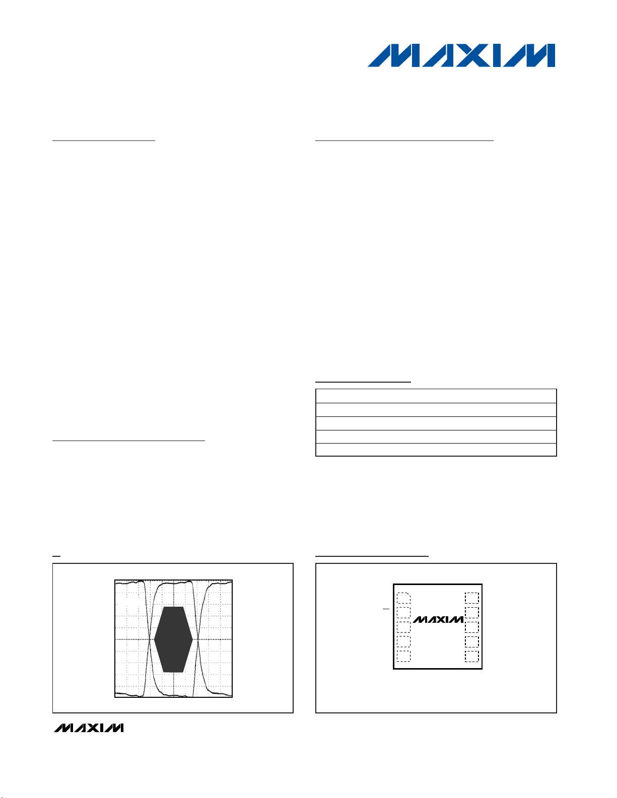
EYE DIAGRAM
500ps/div
V+ =3.3V
I
BIAS = 9mA
f = 240MHz
USB 2.0
HIGH SPEED
TRANSMIT
TEMPLATE
V
NO1OUT
100mV/div
V
NO2OUT
Typical Operating Characteristics
Pin Configurations continued at end of data sheet.
Page 2
High-/Full-Speed USB 2.0 Switches
2 _______________________________________________________________________________________
ABSOLUTE MAXIMUM RATINGS
ELECTRICAL CHARACTERISTICS
(V+ = +3V to +3.6V, TA= T
MIN
to T
MAX
, unless otherwise noted. Typical values are at V+= 3.3V, TA= +25°C.) (Note 2)
Stresses beyond those listed under “Absolute Maximum Ratings” may cause permanent damage to the device. These are stress ratings only, and functional
operation of the device at these or any other conditions beyond those indicated in the operational sections of the specifications is not implied. Exposure to
absolute maximum rating conditions for extended periods may affect device reliability.
Note 1: Signals on IN, SHDN or SHDN/EN exceeding V+ or GND are clamped by internal diodes. Limit forward-diode current to
maximum current rating.
Voltages Referenced to GND
V+ .............................................................................-0.3V to +4V
IN, SHDN, SHDN/EN (Note 1) ......................-0.3V to (V+ + 0.3V)
COM_, NO_, NC_ ..................................................-0.5V to +5.5V
Continuous Current (COM_ to NO_/NC_) ......................±120mA
Peak Current, (COM_ to NO_/NC_)
(pulsed at 1ms 10% duty cycle).................................±240mA
Continuous Power Dissipation (T
A
= +70°C)
8-Pin µDFN (derate 5.0mW/°C above +70°C) .............400mW
10-Pin µDFN (derate 5.3mW/°C above +70°C) ........423.7mW
Operating Temperature Range ..........................-40°C to +85°C
Junction Temperature .....................................................+150°C
Storage Temperature Range .............................-65°C to +150°C
Lead Temperature (soldering, 10s) .................................+300°C
MAX4906/MAX4606F/MAX4907/MAX4907F
PARAMETER
CONDITIONS
UNITS
ANALOG SWITCH
Analog Signal Range
V
NC _
SHDN or SHDN/EN = 0 (Note 3) 0 V+ V
Fault-Protection Trip Threshold V
FP
3.6 4.0 V
TA = +25°C 4 7
On-Resistance R
ON
I
COM_
= -40mA,
0V ≤ V
COM_
≤ V+,
8
Ω
TA = +25°C 4 10
On-Resistance During Shutdown
R
ONSH
I
C OM _
= - 40m A,
0V ≤ V
C OM _
≤ 1.5V ,
S H D N = V +
13
Ω
TA = +25°C 0.7 1.2
On-Resistance Match Between
Channels
ΔR
ON
V+ = 3.0V,
I
COM_
= -40mA,
1.5
Ω
On-Resistance Flatness
)
V+ = 3.0V, I
COM_
= -40mA,
V
COM_
= 1.5V, 3.0V (Note 5)
1.0 Ω
Off-Leakage Current
)
V+ = 3.6V, V
COM_
= 0.3V, 3.3V;
V
NO_
or V
NC_
= 3.3V, 0.3V
-1 +1 µA
On-Leakage Current
)
V+ = 3.6V, V
COM
= 0.3V, 3.3V;
V
NO_
or V
NC_
= 0.3V, 3.3V, or floating
-1 +1 µA
SWITCH AC PERFORMANCE
On-Channel -3dB Bandwidth BW RL = RS = 50Ω, signal = 0dBm, Figure 1
MHz
f = 10MHz; V
NO_
, V
NC_
= 1V
P-P
;
R
L
= RS = 50Ω, Figure 1
-60
f = 250MHz; V
NO_
, V
NC_
= 1V
P-P
;
R
L
= RS = 50Ω, Figure 1
-32
Off-Isolation V
ISO
f = 500MHz; V
NO_
, V
NC_
= 1V
P-P
;
R
L
= RS = 50Ω, Figure 1
-26
dB
SYMBOL
V
_,V
NO_
,
COM
MIN TYP MAX
R
FLAT (ON
I
COM_(OFF
I
COM_(ON
SHDN or SHDN/EN = 0
( M AX 4907/M AX 4907F)
V
= 1.5V (Note 4)
COM_
= T
T
A
T
A
T
A
to T
MIN
MAX
= T
to T
MIN
MAX
= T
to T
MIN
MAX
1000
Page 3
MAX4906/MAX4606F/MAX4907/MAX4907F
High-/Full-Speed USB 2.0 Switches
_______________________________________________________________________________________ 3
ELECTRICAL CHARACTERISTICS (continued)
(V+ = +3V to +3.6V, TA= T
MIN
to T
MAX
, unless otherwise noted. Typical values are at V+ = 3.3V, TA= +25°C.) (Note 2)
PARAMETER
CONDITIONS
UNITS
f = 10MHz; V
NO_
, V
NC_
= 1V
P-P
;
R
L
= RS = 50Ω, Figure 1
-59
f = 250MHz; V
NO_
, V
NC_
= 1V
P-P
;
R
L
= RS = 50Ω, Figure 1
-31
Crosstalk (Note 6) V
CT
f = 500MHz; V
NO_
, V
NC_
= 1V
P-P
;
R
L
= RS = 50Ω, Figure 1
-25
dB
SWITCH DYNAMICS
NO_, NC_ Off-Capacitance C
(OFF)
f = 1MHz, Figure 2 (Note 7) 2 4 pF
MAX4906ELB,
MAX4906FELB
69
Switch On-Capacitance C
(ON)
f = 1MHz, Figure 2
(Note 7)
MAX4907ELA,
MAX4907FELA
47
pF
MAX4906ELB,
MAX4906FELB
0.4
Switch On-Capacitance Matching
C
ONM
f = 1MHz (Note 7)
MAX4907ELA,
MAX4907FELA
0.3
pF
Turn-On Time t
ON
V
N O
_, V
N C
_ = 1.5V ; RL = 300Ω , C L = 35p F,
V
IH
= V + , V IL = 0V , S H D N or S H D N /EN = 0V ,
Fi g ur e 3
60 ns
Turn-Off Time t
OFF
VNO_, VNC_ = 1.5V; RL = 300Ω, CL = 35pF,
Figure 3; TA = +25°C
30 ns
Propagation Delay
RL = RS = 50Ω, Figure 4
ns
Fault-Protection Response Time t
FP
V
COM_
= 0 to 5V step,
R
L
= RS = 50Ω, Figure 5
3.0 µs
Fault-Protection Recovery Time t
FPR
V
COM_
= 5V to 3V step,
R
L
= RS = 50Ω, Figure 5
2µs
Output Skew Between Switches t
SK(o)
Skew between switch 1 and switch 2, RL =
R
S
= 50Ω, Figure 4 (Note 7)
50 100 ps
Output Skew Same Switch t
SK(p)
Skew between opposite transitions in same
switch, R
L
= RS = 50Ω, Figure 4 (Note 7)
50 100 ps
SYMBOL
MIN TYP MAX
VIH = V+, VIL = 0V, SHDN or SHDN/EN = 0V,
t
PLH_,tPHL
0.25
Page 4
MAX4906/MAX4606F/MAX4907/MAX4907F
High-/Full-Speed USB 2.0 Switches
4 _______________________________________________________________________________________
ELECTRICAL CHARACTERISTICS (continued)
(V+ = +3V to +3.6V, TA= T
MIN
to T
MAX
, unless otherwise noted. Typical values are at V+ = 3.3V, TA= +25°C.) (Note 2)
PARAMETER
CONDITIONS
UNITS
Total Harmonic Distortion Plus
Noise
V
COM_
= 2V
P-P
, RL = 600Ω, f = 20Hz to
20kHz
%
Charge Injection Q
V
GEN
= 1.5V, R
GEN
= 0Ω, CL = 100pF,
Figure 6
5pC
SWITCH LOGIC
Logic-Input-Voltage Low V
IL
0.4 V
Logic-Input-Voltage High V
IH
1.1 V
Input-Logic Hysteresis V
HYST
mV
Input Leakage Current I
IN
V+ = 3.6V, VIN = 0 or V+ -1 +1 µA
Operating Supply-Voltage Range
V+ 3.0 3.6 V
Quiescent Supply Current I+
V+ = 3.6V, V
IN
= 0 or V+, SHDN or
SHDN/EN = 0
300 µA
Quiescent Supply Current During
Shutdown
I+
V+ = 3.6V, V
IN
= 0 or V+, SHDN or
SHDN/EN = V+
2µA
Note 2: All units are 100% production tested at TA= +25°C. Limits over the operating temperature range are guaranteed by design
and not production tested.
Note 3: The switch will turn off for voltages above (V
FP
); therefore, protecting downstream circuits in case of a fault condition
(MAX4906F/MAX4907F).
Note 4: ΔR
ON(MAX)
= | R
ON(CH1) – RON(CH2)
|
Note 5: Flatness is defined as the difference between the maximum and minimum value of on-resistance, as measured over
specified analog signal ranges.
Note 6: Between any two switches.
Note 7: Switch off-capacitance, switch on-capacitance, output skew between switches, and output skew same-switch limits are not
production tested; design guaranteed by bench characterization.
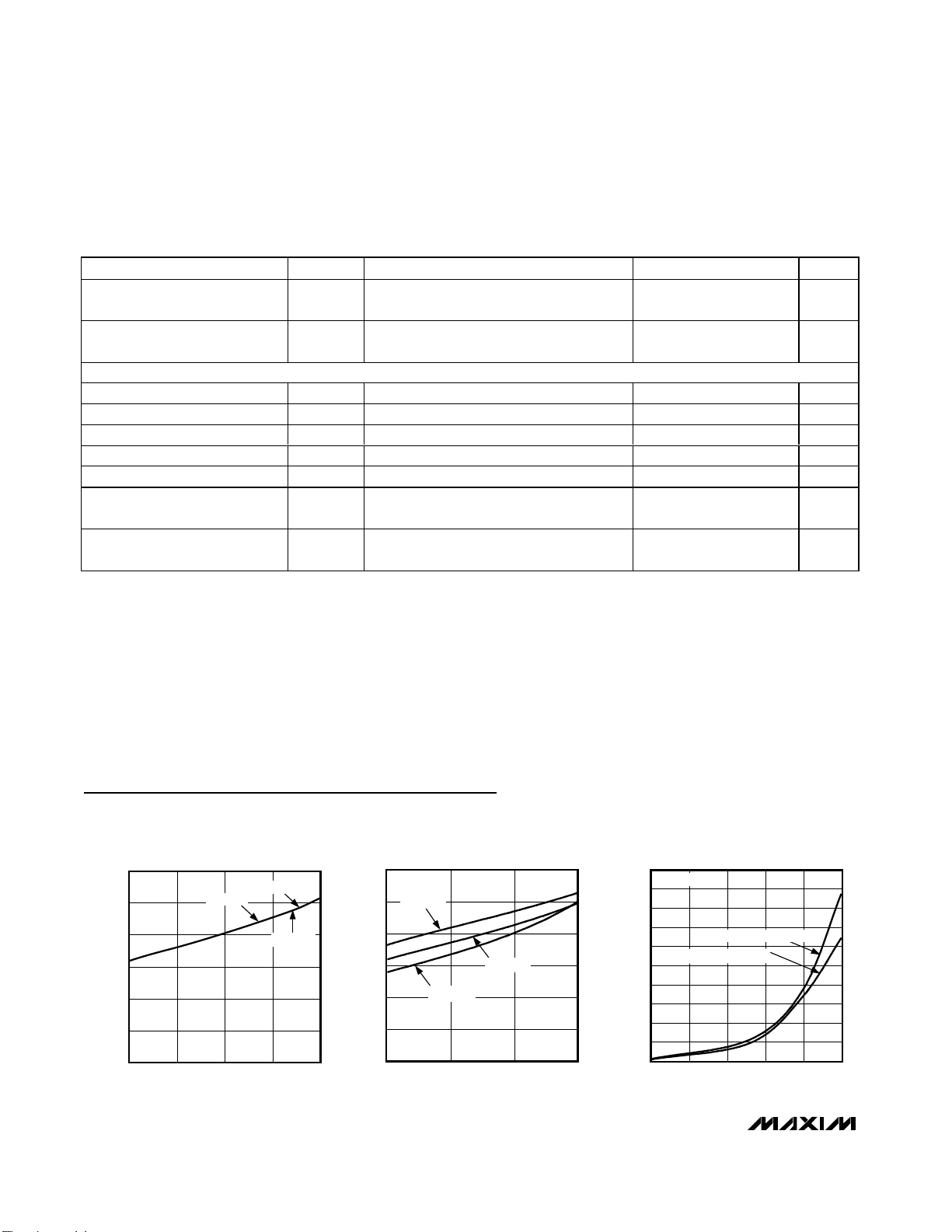
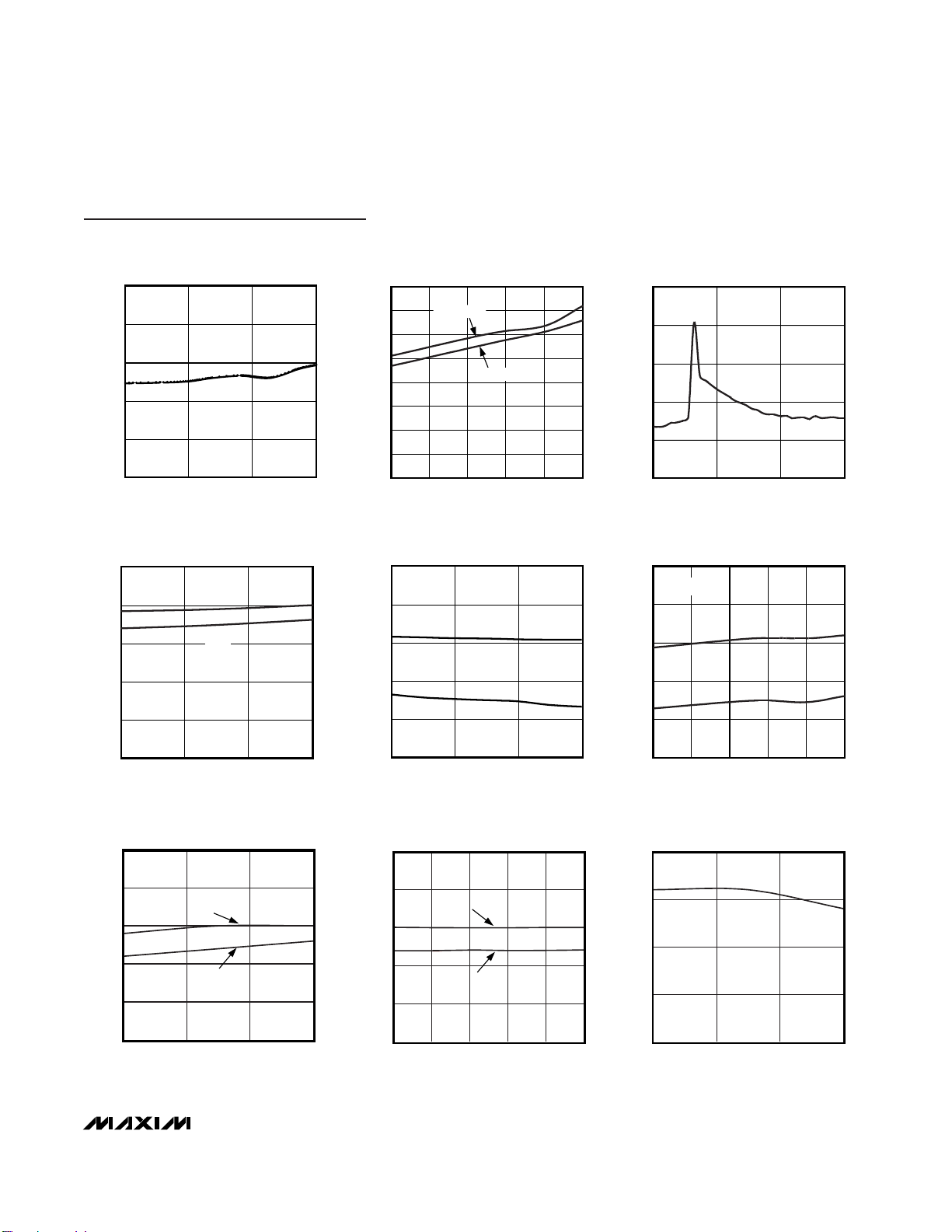
Typical Operating Characteristics
(TA = +25°C, unless otherwise noted.)
0
1500
1000
500
2000
2500
3000
3500
4000
4500
5000
-40 10-15 35 60 85
LEAKAGE CURRENT vs. TEMPERATURE
MAX4906 toc03
TEMPERATURE (°C)
LEAKAGE CURRENT (pA)
COM ON-LEAKAGE
COM OFF-LEAKAGE
V+ = 3.6V
0
2
1
4
3
5
6
01.80.9 2.7 3.6
ON-RESISTANCE vs. V
COM
MAX4906 toc01
V
COM
(V)
R
ON
(Ω)
V+ = 3.3V
V+ = 3.0V
V+ = 3.6V
0
2
1
4
3
5
6
0 1.1 2.2 3.3
MAX4906 toc02
V
COM
(V)
ON-RESISTANCE vs. V
COM
R
ON
(Ω)
TA = +40°C
TA = +25°C
TA = +85°C
V+ = 3.3V
SYMBOL
MIN TYP MAX
THD+N
0.03
100
120
Page 5
MAX4906/MAX4606F/MAX4907/MAX4907F
High-/Full-Speed USB 2.0 Switches
_______________________________________________________________________________________ 5
100
110
130
120
140
150
QUIESCENT SUPPLY CURRENT
vs. LOGIC LEVEL
MAX4906 toc06
LOGIC LEVEL (V)
QUIESCENT SUPPLY CURRENT (μA)
0 2.21.1 3.3
V+ = 3.3V
O
0.2
0.6
0.4
0.8
1
LOGIC THRESHOLD vs. SUPPLY VOLTAGE
MAX4906 toc07
SUPPLY VOLTAGE (V)
LOGIC THRESHOLD (V)
3.0 3.43.2 3.6
V
IH
V
IL
O
10
30
20
40
50
TURN-ON/OFF TIME
vs. SUPPLY VOLTAGE
MAX4906 toc08
SUPPLY VOLTAGE (V)
t
ON
/t
OFF
(ns)
3.0 3.43.2 3.6
t
ON
t
OFF
0
10
30
20
40
50
-40 10-15 35 60 85
TURN-ON/OFF TIME
vs. TEMPERATURE
MAX4906 toc09
TEMPERATURE (°C)
t
ON
/t
OFF
(ns)
t
ON
t
OFF
V+ = 3.3V
200
210
230
220
240
250
RISE/FALL-TIME PROPAGATION DELAY
vs. SUPPLY VOLTAGE
MAX4906 toc10
SUPPLY VOLTAGE (V)
OUTPUT RISE/FALL -TIME DELAY (ps)
33.43.2 3.6
..0
T
PLH
T
PHL
200
210
230
220
240
250
-40 10-15 35 60 85
RISE/FALL-TIME PROPAGATION DELAY
vs. TEMPERATURE
MAX4906 toc11
TEMPERATURE (°C)
OUTPUT RISE/FALL -TIME DELAY (ps)
V+ = 3V
T
PLH
T
PHL
0
10
5
-5
-10
3.0 3.43.2 3.6
SAME SWITCH OUTPUT SKEW
vs. SUPPLY VOLTAGE
XMAX4906 toc12
SUPPLY VOLTAGE (V)
OUTPUT SKEW (ps)
Typical Operating Characteristics (continued)
(TA = +25°C, unless otherwise noted.)
0
2
6
4
8
10
CHARGE INJECTION vs. V
COM
MAX4906 toc04
VCOM (V)
CHARGE INJECTION (pC)
02.21.1 3.3
CL = 100pF
V+ = 3.3V
0
20
40
60
80
100
120
140
160
-40 -15 10 35 60 85
QUIESCENT SUPPLY CURRENT
vs. TEMPERATURE
MAX4906 toc05
TEMPERATURE (°C)
QUIESCENT SUPPLY CURRENT (μA)
V+ = 3.6V
V+ = 3.0V
Page 6

MAX4906/MAX4606F/MAX4907/MAX4907F
High-/Full-Speed USB 2.0 Switches
6 _______________________________________________________________________________________
FREQUENCY RESPONSE
MAX4906 toc13
FREQUENCY (MHz)
ON-LOSS (dB)
10010
-90
-80
-70
-60
-50
-40
-30
-20
-10
0
-100
11000
CROSS-TALK
OFF-ISOLATION
ON-LOSS
OUTPUT SKEW BETWEEN SWITCHES
vs. SUPPLY VOLTAGE
MAX4906 toc13
SUPPLY VOLTAGE (V)
OUTPUT SKEW (ps)
3.43.2
-5
0
5
10
-10
3.0 3.6
TOTAL HARMONIC DISTORTION
PLUS NOISE vs. FREQUENCY
MAX4906 toc15
FREQUENCY (Hz)
THD+N (%)
10k1k100
0.1
10 100k
1
0.01
V+ = 3.3V
R
L
= 600
Ω
Typical Operating Characteristics (continued)
(TA = +25°C, unless otherwise noted.)
Page 7

MAX4906/MAX4606F/MAX4907/MAX4907F
High-/Full-Speed USB 2.0 Switches
Pin Description
PIN
MAX4906/
MAX4906F
NAME
FUNCTION
1 8 IN Digital Control Input. IN controls switch 1 and switch 2.
2—
S hutd ow n and E nab l e Inp ut. D r i ve S H D N /EN hi g h to consum e m i ni m um cur r ent and to p ut the
d evi ce i n hi g h- i m p ed ance m od e. D r i ve the S H D N /EN l ow for nor m al op er ati on.
3 2 GND Ground
43
Analog Switch 1—Common Terminal
54
Analog Switch 2—Common Terminal
6 5 NO2 Analog Switch 2—Normally Open Terminal
7 6 NO1 Analog Switch 1—Normally Open Terminal
8 — NC2 Analog Switch 2—Normally Closed Terminal
9 — NC1 Analog Switch 1—Normally Closed Terminal
10 7 V+
Positive-Supply Voltage Input. Connect V+ to a 3.0V to 3.6V supply voltage. Bypass V+ to
GND with a 0.1µF capacitor.
—1
Shutdown Input. Drive SHDN high to put the device into shutdown mode. For normal
operation, drive SHDN low.
Test Circuits/Timing Diagrams
_______________________________________________________________________________________ 7
Figure 1. On-Loss, Off-Isolation, and Crosstalk
MAX4907/
MAX4907F
S H D N /E N
COM1
COM2
SHDN
10nF
+3.3V
NETWORK
ANALYZER
50Ω
MEAS REF
50Ω 50Ω
0V OR V+
50Ω
IN_
MAX4906/MAX4906F
NC1
MAX4907/MAX4907F
GND
V+
COM1
NO1*
V
IN
V
OUT
MEASUREMENTS ARE STANDARDIZED AGAINST SHORTS AT IC TERMINALS.
OFF-ISOLATION IS MEASURED BETWEEN COM_ AND "OFF" NO_ OR NC_ TERMINAL ON EACH SWITCH.
ON-LOSS IS MEASURED BETWEEN COM_ AND "ON" NO_ OR NC_ TERMINAL ON EACH SWITCH.
CROSSTALK IS MEASURED FROM ONE CHANNEL TO THE OTHER CHANNEL.
SIGNAL DIRECTION THROUGH SWITCH IS REVERSED; WORST VALUES ARE RECORDED.
50Ω
OFF-ISOLATION = 20log
ON-LOSS = 20log
CROSSTALK = 20log
*FOR CROSSTALK THIS PIN IS NO2.
NC2 AND COM2 ARE OPEN.
V
V
V
V
V
V
OUT
IN
OUT
IN
OUT
IN
Page 8

MAX4906/MAX4606F/MAX4907/MAX4907F
High-/Full-Speed USB 2.0 Switches
8 _______________________________________________________________________________________
Test Circuits/Timing Diagrams (continued)
CAPACITANCE
METER
NC_ or
NO_
COM_
GND
IN
V
IL
OR V
IH
10nF
V+
f = 1MHz
V+
MAX4906/MAX4906F
MAX4907/MAX4907F
Figure 2. Channel Off/On-Capacitance
tr < 5ns
tf < 5ns
50%
V
IL
LOGIC
INPUT
R
L
COM_
GND
IN
C
L
INCLUDES FIXTURE AND STRAY CAPACITANCE.
V
OUT
= V
N_ (
R
L
)
RL + R
ON
V
N_
V
IH
t
OFF
0V
NO_
OR NC_
0.9 x V
0UT
0.9 x V
OUT
t
ON
V
OUT
SWITCH
OUTPUT
LOGIC
INPUT
IN DEPENDS ON SWITCH CONFIGURATION;
INPUT POLARITY DETERMINED BY SENSE OF SWITCH.
V+
C
L
V+
V
OUT
MAX4906/MAX4906F
MAX4907/MAX4907F
Figure 3. Switching Time
Page 9

MAX4906/MAX4606F/MAX4907/MAX4907F
High-/Full-Speed USB 2.0 Switches
_______________________________________________________________________________________ 9
IN+
IN-
IN IN
OUT+
OUT-
V
IN+
V
IN-
V
OUT+
V
OUT-
NC1 OR
NO1
NC2 OR
NO2
COM1
COM2
0V
V+
0V
V+
0V
V+
0V
V+
t
PLHX
t
PHLX
t
INRISE
t
OUTRISE
t
OUTFALL
RISE-TIME PROPAGATION DELAY = t
PHLX
OR t
PHLY
FALL-TIME PROPAGATION DELAY = t
PHLX
OR t
PHLY
t
SK(O)
= |t
PHLX
- t
PHLY
| OR |t
PHLX
- t
PHLY
|
t
SK(P)
= |t
PHLX
- t
PHLX
| OR |t
PHLY
- t
PHLY
|
50%
50%
50%
50%
90%
10% 10%
90%
10% 10%
MAX4906/MAX4906F
MAX4907/MAX4907F
R
L
R
L
50%
50%
50%
50%
t
INFALL
90%
90%
t
PHLY
t
PLHY
R
S
R
S
VIL TO V
IH
Figure 4. Output Signal Skew, Rise/Fall Time, Propagation Delay
_______________________________________________________________________________________ 9
Test Circuits/Timing Diagrams (continued)
Page 10
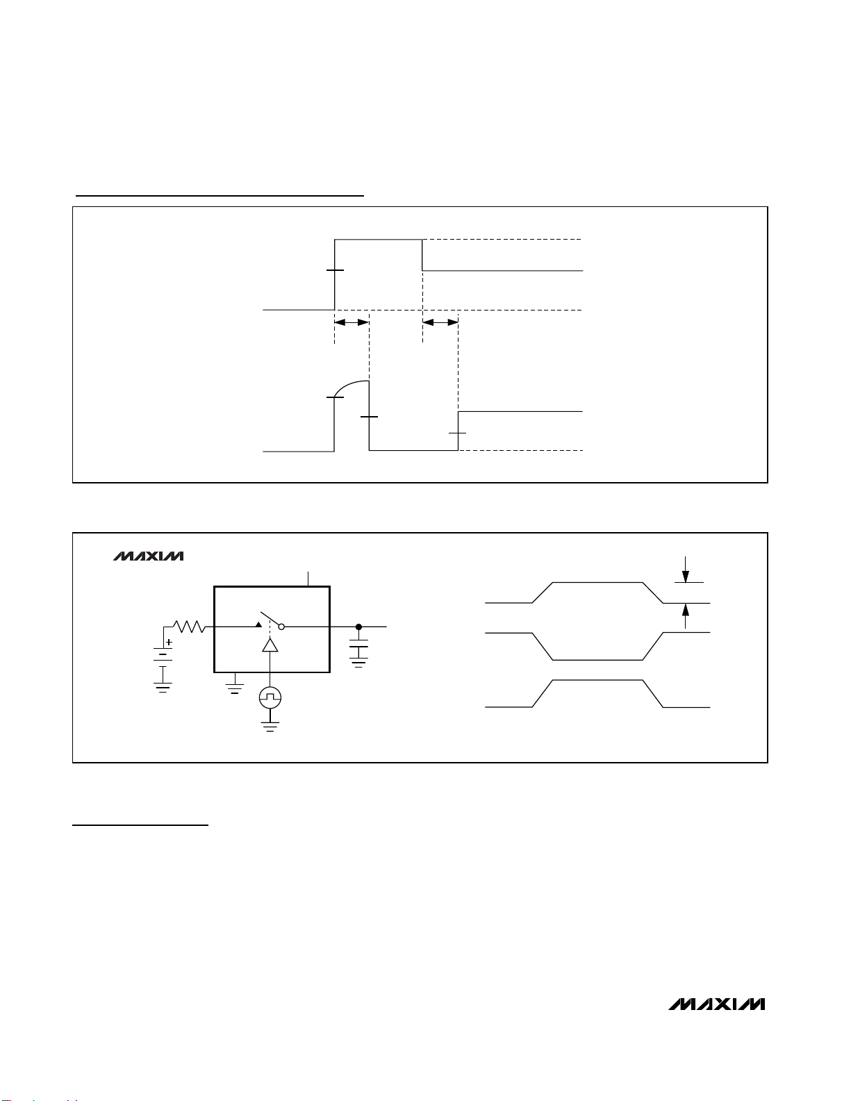
MAX4906/MAX4606F/MAX4907/MAX4907F
High-/Full-Speed USB 2.0 Switches
10 ______________________________________________________________________________________
2.5V
V
PF
t
PF
t
FPR
5V
3V
0V
3V
1.5V
2.5V
0V
VCOM_
VNC_
VNO_
Figure 5. MAX4906F/MAX4907F Fault-Protection Response/Recovery Time
Test Circuits/Timing Diagrams (continued)
V
GEN
GND
COM_
C
L
V
OUT
V+
V
OUT
IN
OFF
ON
OFF
ΔV
OUT
Q = (ΔV
OUT
)(CL)
NC_
LOGIC INPUT WAVEFORMS INVERTED FOR SWITCHES
THAT HAVE THE OPPOSITE LOGIC SENSE.
OFF
ON
OFF
IN
V
IL
TO V
IH
V+
R
GEN
IN
MAX4906/MAX4906F
MAX4907/MAX4907F
OR NO_
Figure 6. Charge Injection
Detailed Description
The MAX4906/MAX4906F/MAX4907/MAX4907F analog
switches are targeted for USB 2.0 high-speed
(480Mbps) switching applications. These devices still
meet USB low- and full-speed requirements and are
suitable for 10/100 Ethernet switching. The MAX4906/
MAX4906F feature two SPDT switches, while the
MAX4907/MAX4907F feature two SPST switches. The
MAX4907/MAX4907F switch configurations have a low
7Ω (max) on-resistance and 7pF (max) on-capacitance.
The MAX4906/MAX4906F/MAX4907/MAX4907F are fully
specified to operate from a single +3.0V to +3.6V supply
and are available with +5.5V fault protection (MAX4906F/
MAX4907F). When operating from a +3.0V to +3.6V supply, the low threshold of these devices permits them to
be used with logic levels as low as 1.4V.The
MAX4906/MAX4906F/MAX4907/MAX4907F are based
on a charge-pump-assisted n-channel architecture and
thus operate at 300µA (max) quiescent current. These
devices all feature a shutdown input to reduce the quiescent current to less than 2µA (max).
Page 11

MAX4906/MAX4606F/MAX4907/MAX4907F
High-/Full-Speed USB 2.0 Switches
______________________________________________________________________________________ 11
Functional Diagram/Truth Table
IN
V+ V+
NC1
NO1
NC2
NO2
COM1
COM2
GND
SHDN/EN
SHDN I N
1
1
00 OFF
OFF
ON
IN
NO1
NO2
COM1
COM2
GND
SHDN
COM1- NO1
COM2- NO1
0
1
ON0
1
MAX4906/MAX4906F
MAX4907/MAX4907F
SHDN/EN IN
1
1
00OFF
MAX4906/MAX4906F
MAX4907/MAX4907F
OFF
NO1
NO2
x
ON
ON
OFF
NC1
NC2
OFF
0
Digital Control Input
The MAX4906/MAX4906F/MAX4907/MAX4907F provide
a single-digit control logic input, IN. IN controls the
position of the switches as shown in the Functional
Diagram/Truth Table. Driving IN rail-to-rail minimizes
power consumption. With a +3.0V to +3.6V supply voltage range, these devices are +1.4V logic compatible.
Analog Signal Levels
The on-resistance of the MAX4906/MAX4906F/
MAX4907/MAX4907F is very low and stable as the analog input signals are swept from ground to V+ (see the
Typical Operating Characteristics). These switches are
bidirectional, allowing NO_, NC_, and COM_ to be configured as either inputs or outputs.
Overvoltage Fault Protection
The MAX4906F and MAX4907F feature +5.5V fault protection to COM1 and COM2. Fault protection prevents
these switches from being damaged due to shorts to
the USB bus voltage rail.
Shutdown Mode
The MAX4906/MAX4906F feature a shutdown mode
that reduces the quiescent current supply to less than
2µA. Drive SHDN/EN high to place the devices in highimpedance mode. When SHDN/EN is driven low, the
devices are normal in operation.
The MAX4907/MAX4907F feature a SHDN input that
reduces the quiescent current supply to less than 2µA.
Drive SHDN high to place the devices in low current
mode. The devices can be used in low current mode, but
with a reduced analog voltage range of 0 < V
ANALOG
<
1.5V and reduced performance. When SHDN is driven
low, the MAX4907/MAX4907F are in normal operation.
Applications Information
USB Switching
The MAX4906/MAX4906F/MAX4907/MAX4907F analog
switches are fully compliant with the USB 2.0 specification. The low on-resistance and low on-capacitance of
these switches make them ideal for high-performance
switching applications. The MAX4906/MAX4906F are
Page 12
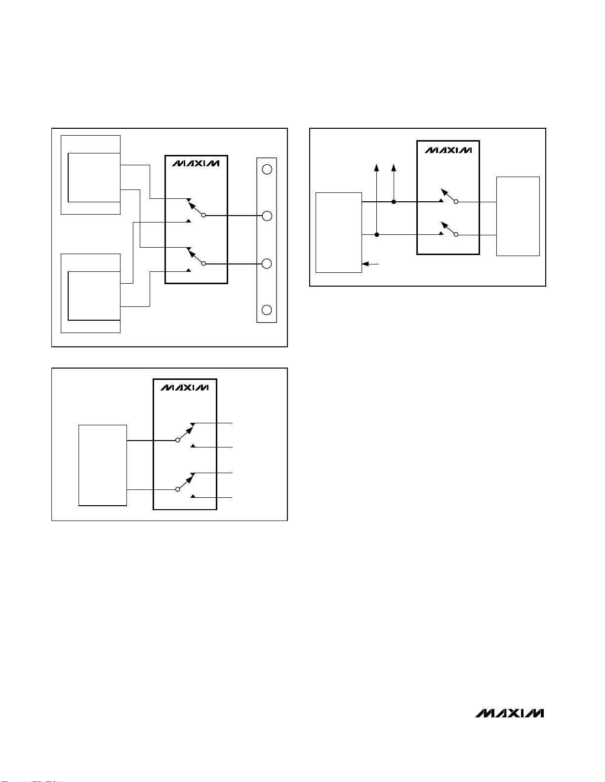
MAX4906/MAX4606F/MAX4907/MAX4907F
High-/Full-Speed USB 2.0 Switches
12 ______________________________________________________________________________________
ideal for routing USB data lines (see Figure 7) and for
applications that require switching between multiple
USB hosts (see Figure 8). The MAX4907/MAX4907F
can be used in applications that require different data
types to share the same pins (see Figure 9); however,
the shared device must be capable of going into the tristate mode. The MAX4906F/MAX4907F also feature
+5.5V fault protection to guard systems against shorts
to the USB bus voltage. The fault-protected versions
are recommended for all USB applications.
Ethernet Switching
The wide bandwidth of the MAX4906/MAX4906F/
MAX4907/MAX4907F meets the needs of 10/100 Ethernet
switching. These devices switch the signals from two
interface transformers and connect the signals to a single
10/100 Base-T Ethernet PHY, simplifying docking station
design and reducing manufacturing costs.
Power-Supply Sequencing
Caution: Do not exceed the absolute maximum ratings because stresses beyond the listed ratings
may cause permanent damage to the device.
Proper power-supply sequencing is recommended for
all CMOS devices. Always apply V+ before applying
analog signals, especially if the analog signal is not
current limited.
Layout
High-speed switches require proper layout and design
procedures for optimum performance. Keep designcontrolled-impedance PC board traces as short as possible. Ensure that bypass capacitors are as close to the
device as possible. Use large ground planes where
possible.
V
BUS
ASIC I
ASIC II
USB
TRANSCEIVER
D+
D-
D+
NC1
NO1
NC2
NO2
D-
D+
D-
GND
USB
CONNECTOR
COM1
COM2
USB
TRANSCEIVER
MAX4906/
MAX4906F
Figure 7. MAX4906/MAX4906F USB Data Routing
Figure 8. MAX4906/MAX4906F Switching Between Multiple
USB Hosts
DATA
SPI/GPIO
DEVICE
CLOCK
EN
TRI-STATE
ENABLE
SHARED
DATA PINS
COM1
COM2
MAX4907/
MAX4907F
USB
TRANSCEIVER
NO1
NO2
Figure 9. MAX4907/MAX4907F USB/SPI/GPIO Switch
MAX4906/
MAX4906F
USB
TRANSCEIVER
COM1
COM2
NC1
NO1
NC2
NO2
USB
USB
USB
USB
+
0
+
1
-
0
-
1
Page 13
MAX4906/MAX4606F/MAX4907/MAX4907F
High-/Full-Speed USB 2.0 Switches
______________________________________________________________________________________ 13
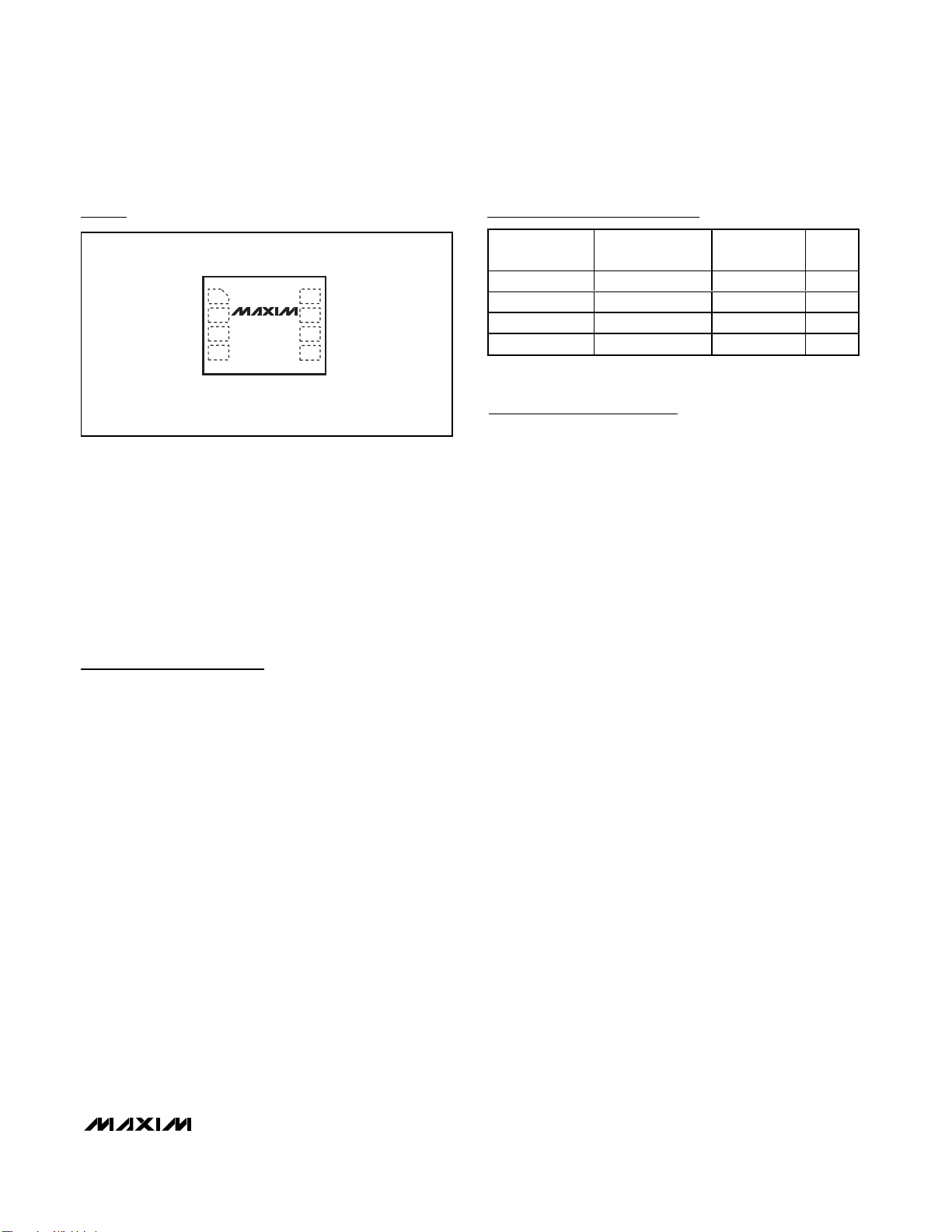
PART
CONFIGURATION
FAULT
TOP
MARK
MAX4906ELB Dual SPDT NO AAB
MAX4906FELB
Dual SPDT YES AAA
MAX4907ELA Dual SPST NO AAE
MAX4907FELA
Dual SPST YES
AAD
Selector Guide
Chip Information
PROCESS: BiCMOS
TOP VIEW
1
2
3
4
8
7
6
5
IN
V+
NO1
NO2COM2
COM1
GND
SHDN
MAX4907
MAX4907F
μDFN
Pin Configurations (continued)
Revision History
Pages changed at Rev 2: 1, 2, 3, 7, 11, 14
PROTECTION
Page 14

MAX4906/MAX4606F/MAX4907/MAX4907F
High-/Full-Speed USB 2.0 Switches
Maxim cannot assume responsibility for use of any circuitry other than circuitry entirely embodied in a Maxim product. No circuit patent licenses are
implied. Maxim reserves the right to change the circuitry and specifications without notice at any time.
14 ____________________Maxim Integrated Products, 120 San Gabriel Drive, Sunnyvale, CA 94086 408-737-7600
© 2007 Maxim Integrated Products is a registered trademark of Maxim Integrated Products. Inc.
6, 8, 10L UDFN.EPS
EVEN TERMINAL
L
C
ODD TERMINAL
L
C
L
e
L
A
e
E
D
PIN 1
INDEX AREA
b
e
A
b
N
SOLDER
MASK
COVERAGE
A A
1
PIN 1
0.10x45∞
L
L1
(N/2 -1) x e)
XXXX
XXXX
XXXX
SAMPLE
MARKING
A1
A2
7
A
1
2
21-0164
PACKAGE OUTLINE,
6, 8, 10L uDFN, 2x2x0.80 mm
-DRAWING NOT TO SCALE-
COMMON DIMENSIONS
SYMBOL MIN. NOM.
A
0.70 0.75
A1
D 1.95 2.00
E
1.95 2.00
L
0.30 0.40
PKG. CODE N e b
PACKAGE VARIATIONS
L1
6L622-1 0.65 BSC 0.30±0.05
0.25±0.050.50 BSC8L822-1
0.20±0.030.40 BSC10L1022-1
2.05
0.80
MAX.
0.50
2.05
0.10 REF.
(N/2 -1) x e
1.60 REF.
1.50 REF.
1.30 REF.
A2
-
-DRAWING NOT TO SCALE-
A
2
2
21-0164
PACKAGE OUTLINE,
6, 8, 10L uDFN, 2x2x0.80 mm
0.15 0.20 0.25
0.020 0.025 0.035
Package Information
(The package drawing(s) in this data sheet may not reflect the most current specifications. For the latest package outline information
go to www.maxim-ic.com/packages
.)
 Loading...