

Page 1
现货库存、技术资料、百科信息、热点资讯,精彩尽在鼎好!
General Description
The MAX4901–MAX4905 switches feature negative
signal capability that allows signals below ground to pass
through without distortion. The MAX4901/MAX4902 are a
dual SPST (single-pole/single-throw) and the MAX4903/
MAX4904/MAX4905 are a single SPDT (singlepole/double-throw) configuration. These analog switches
operate from a single +1.8V to +5.5V supply and have
low 0.6Ω on-resistance, making them ideal for switching
audio signals.
The MAX4905 includes a comparator that can be used
for headphone detection or mute/send key function. The
MAX4902/MAX4904/MAX4905 have internal shunt resistors to automatically discharge any capacitance at the
NO_ and NC connection points. This reduces click-andpop sounds that occur when switching audio signals
between pre-charged points. A break-before-make feature and auto-discharge also help to reduce popping.
These SPST and SPDT switches are available in
space-saving 8-pin TDFN and 9-bump UCSP™ packages and operate over the -40°C to +85°C extended
temperature range.
Applications
Features
♦ Distortion-Free Signal Throughput Down
to VCC- 5.5V
♦ Comparator for Headphone or
Mute Detection (MAX4905)
♦ Clickless Switches with Internal Shunt Resistors
(MAX4902/MAX4904/MAX4905)
♦ 0.6Ω (typ) Low On-Resistance (R
ON
)
♦ 0.25Ω On-Resistance Flatness
♦ +1.8V to +5.5V Supply Voltage
♦ 0.04% THD
MAX4901–MAX4905
Low-R
ON
, Dual-SPST/Single-SPDT Clickless
Switches with Negative Rail Capability
________________________________________________________________ Maxim Integrated Products 1
19-3775; Rev 2; 5/06
For pricing, delivery, and ordering information, please contact Maxim/Dallas Direct! at
1-888-629-4642, or visit Maxim’s website at www.maxim-ic.com.
Ordering Information/Selector Guide
PART PIN-PACKAGE
TOP MARK
CONFIGURATION
COMPARATOR
SHUNT
PKG CODE
MAX4901EBL-T
AEU 2 x SPST No No B9-1
MAX4901ETA-T
8 TD FN - 8 AOW 2 x SPST No No T833-2
MAX4902EBL-T
AEV 2 x SPST No Yes B9-1
MAX4902ETA-T
8 TD FN - 8AOX 2 x SPST No Yes T833-2
MAX4903EBL-T
AEY 1 x SPDT No No B9-1
MAX4903ETA-T
8 TD FN - 8AOY 1 x SPDT No No T833-2
MAX4904EBL-T
AEW 1 x SPDT No Yes B9-1
MAX4904ETA-T
8 TD FN - 8AOZ 1 x SPDT No Yes T833-2
MAX4905EBL-T
AEX 1 x SPDT Yes Yes B9-1
MAX4905ETA-T
8 TD FN - 8 APA 1 x SPDT Yes Yes T833-2
Note: All devices operate over the -40°C to +85°C operating temperature range.
UCSP is a trademark of Maxim Integrated Products, Inc.
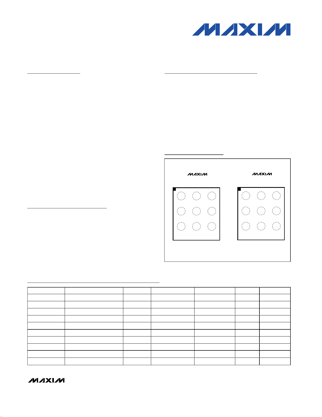
Pin Configurations
3 x 3 UCSP
MAX4901/MAX4902
123
B
C
A
B
C
A
TOP VIEW
BUMPS ON BOTTOM
COM1
NO1 IN1
V
CC
N.C. GND
COM2
NO2
IN2
3 x 3 UCSP
MAX4903/MAX4904/MAX4905
123
V
CC
NO
IN
COM N.C. (CMPO) GND
N.C.
NC
N.C. (CMP-)
( ) MAX4905 ONLY
Pin Configurations continued at end of data sheet.
Cell Phones
PDAs and Handheld Devices
Notebook Computers
MP3 Players
1.5m m x 1.5m m 9 U C S P - 9
1.5m m x 1.5m m 9 U C S P - 9
1.5m m x 1.5m m 9 U C S P - 9
1.5m m x 1.5m m 9 U C S P - 9
1.5m m x 1.5m m 9 U C S P - 9
Page 2
MAX4901–MAX4905
Low-R
ON
, Dual-SPST/Single-SPDT Clickless
Switches with Negative Rail Capability
2 _______________________________________________________________________________________
ABSOLUTE MAXIMUM RATINGS
Stresses beyond those listed under “Absolute Maximum Ratings” may cause permanent damage to the device. These are stress ratings only, and functional
operation of the device at these or any other conditions beyond those indicated in the operational sections of the specifications is not implied. Exposure to
absolute maximum rating conditions for extended periods may affect device reliability.
(All voltages referenced to GND.)
V
CC
, IN_, CMP-......................................................-0.3V to +6.0V
COM_, NO_, NC ................................(V
CC
- 6V) to (VCC+ 0.3V)
CMPO.........................................................-0.3V to (V
CC
+ 0.3V)
Open-Switch Continuous Current NO_, NC
(MAX4902/MAX4904/MAX4905)...................................±30mA
Closed-Switch Continuous Current COM_, NO_, NC.....±100mA
Peak Current COM_, NO_, NC
(Pulsed at 1ms, 50% duty cycle)................................±200mA
Peak Current COM_, NO_, NC
(Pulsed at 1ms, 10% duty cycle)................................±300mA
Continuous Power Dissipation (T
A
= +70°C)
8-Pin TDFN (derate 18.2mW/°C above +70°C) .........1455mW
9-Bump UCSP (derate 5.2mW/°C above +70°C).........412mW
ESD Method 3015.7 .............................................................±2kV
Operating Temperature Range ...........................-40°C to +85°C
Junction Temperature......................................................+150°C
Storage Temperature Range .............................-65°C to +150°C
Lead Temperature (soldering, 10s) .................................+300°C
Bump Temperature (soldering)
Infrared (15s) ...............................................................+220°C
Vapor Phase (60s) .......................................................+215°C
ELECTRICAL CHARACTERISTICS
(V
CC
= +2.7V to +5.5V, TA= -40°C to +85°C, unless otherwise noted. Typical values are at VCC= +3.0V, TA= +25°C, unless other-
wise noted.) (Note 1)
PARAMETER
SYMBOL
CONDITIONS
MIN
TYP
MAX
UNITS
POWER SUPPLY
Power-Supply Range V
CC
1.8 5.5 V
MAX4901–
MAX4904
1
Supply Current I+
V
CC
= 5.5V,
V
IN_
= 0V or V
CC
MAX4905 5 10
µA
ANALOG SWITCH
Analog Signal Range
V
NO
_ VNC,
V
COM_
(Note 2)
V
CC
-
5.5
V
TA = +25°C 0.6 1.0
On-Resistance
R
ON(NC),
)
VCC = 2.7V, V
NC
or V
NO_
= VCC - 5.5V, -1V, 0, 1V,
2V, V
CC; ICOM
= 100mA
(Notes 3, 4)
T
A
= T
MIN
to
T
MAX
1.2
Ω
TA = +25°C
On-Resistance Match Between
Channels
∆R
ON
VCC = 2.7V, I
NO_
or
I
NC
= 100mA or V
NO_
(Notes 3, 4, 5)
T
A
= T
MIN
to
T
MAX
Ω
TA = +25°C
0.5
On-Resistance Flatness R
FLAT
V
C C
= 2.7V, V
N C
or V
NO_
= V
C C
- 5.5V , -1V, 0, 1V,
(Notes 4, 6)
T
A
= T
MIN
to
T
MAX
0.5
Ω
R
ON(NO
2V, VCC; I
= 100mA
COM
0.001
0.01 0.25
0.25
V
CC
0.30
Page 3
MAX4901–MAX4905
Low-R
ON
, Dual-SPST/Single-SPDT Clickless
Switches with Negative Rail Capability
_______________________________________________________________________________________ 3
ELECTRICAL CHARACTERISTICS (continued)
(V
CC
= +2.7V to +5.5V, TA= -40°C to +85°C, unless otherwise noted. Typical values are at VCC= +3.0V, TA= +25°C, unless other-
wise noted.) (Note 1)
PARAMETER
CONDITIONS
UNITS
Shunt Resistance R
SH
I
NO_
or I
NC
= 10mA,
V
CC
= 2.7V
(MAX4902/MAX4904/
MAX4905)
TA = T
MIN
to T
MAX
30 50 Ω
-6 +6
NO_, NC Off-Leakage Current
),
)
VCC = 2.7V, switch open; V
NC
or V
NO_
= -2.5V, +2.5V; V
COM_
= +2.5V, -2.5V (MAX4901/
MAX4903) (Notes 3, 7)
TA = T
MIN
to T
MAX
nA
-6 +6
COM_ Off-Leakage Current
)
VCC = 2.7V, switch open;
V
NC
or V
NO_
= -2.5V, +2.5V;
V
COM_
= -2.5V, +2.5V
(MAX4901) (Note 3)
T
A
= T
MIN
to T
MAX
nA
-6 +6
COM_ On-Leakage Current
)
VCC = 2.7V, switch closed;
V
NC
or V
NO_
= -2.5V, +2.5V,
or unconnected ; V
C OM _
= - 2.5V ,
TA = T
MIN
to T
MAX
nA
DYNAMIC CHARACTERISTICS
Turn-On Time
t
ON
VCC = 2.7V, VNO = 1.5V, V
IN_
= 0V to VCC;
V
NC
= 1.5V, V
IN_
= VCC to 0; RL = 50Ω,
C
L
= 5pF (Figure 1)
25
ns
Turn-Off Time t
OFF
VCC = 2.7V, VNO_ = 1.5V, V
IN_
= VCC to 0;
V
NC
= 1.5V, V
IN_
= 0 to VCC; RL = 50Ω,
C
L
= 5pF (Figure 1)
15
ns
210
Break-Before-Make Time Delay
(MAX4903/MAX4904/MAX4905)
t
BBM
VCC = 2.7V, V
NO_
= 1.5V,
V
IN_
= VCC to 0; VNC = 1.5V,
V
IN_
= 0 to VCC; RL = 50Ω,
C
L
= 5pF (Figure 2)
T
A
= T
MIN
to T
MAX
1
ns
Charge Injection Q
pC
Off-Isolation (Note 8) V
ISO
f = 100kHz, V
COM_
= 1V
RMS
,
R
L
= 50Ω, CL = 5pF (Figure 4)
dB
Crosstalk V
CT
f = 100kHz, V
COM_
= 1V
RMS
,
R
L
= 50Ω, CL = 5pF (Figure 4)
dB
Power-Supply Rejection Ratio PSRR
f = 10kHz, V
COM_
= 1V
RMS
,
R
L
= 50Ω, CL = 5pF
60 dB
On-Channel -3dB Bandwidth BW
Signal = 0dBm, R
L
= 50Ω,
C
L
= 5pF (Figure 4)
27
MHz
Total Harmonic Distortion THD
f = 20Hz to 20kHz, V
COM
= 0.5V
P-P
,
DC bias = 0, R
L
= 32Ω
%
SYMBOL
I
NO_(OFF
I
NC (OFF
I
COM_(OFF
I
COM_(ON
+2.5V or unconnected (Note 3)
TA = +25°C
TA = +25°C
TA = +25°C
MIN TYP MAX
-50 +50
-50 +50
-50 +50
100
V
= 0V, RS = 0Ω, CL = 1.0nF (Figure 3) 125
COM_
TA = +25°C
-70
-75
0.04
100
Page 4
MAX4901–MAX4905
Low-R
ON
, Dual-SPST/Single-SPDT Clickless
Switches with Negative Rail Capability
4 _______________________________________________________________________________________
PARAMETER
SYMBOL
CONDITIONS
MIN
TYP
MAX
UNITS
NO_, NC Off-Capacitance
)
)
f = 1MHz, V
COM
= 0.5V
P-P
, DC bias = 0
(Figure 5)
40 pF
COM On-Capacitance
)
f = 1MHz, V
COM
= 0.5V
P-P
, DC bias = 0
(Figure 5)
pF
DIGITAL I/O (IN_)
VCC = 2.7V to 3.6V 1.4
Input Logic-High Voltage V
IH
VCC = 4.2V to 5.5V 2.0
V
VCC = 2.7V to 3.6V 0.5
Input Logic-Low Voltage V
IL
VCC = 4.2V to 5.5V 0.8
V
Input Leakage Current I
IN
V
IN_
= 0V or V
CC
-1 +1 µA
COMPARATOR (MAX4905)
Comparator Threshold
V
Comparator Output-High Voltage
I
SOURCE
= 1mA
V
CC
V
Comparator Output-Low Voltage
I
SINK
= 1mA 0.4 V
Comparator Input Leakage
V
CMP
- = 0 to 2.7V
nA
Comparator Switching Time
V
CC
= 2.7V, V
CMP-
= 0V to VCC, from 50%
of V
CMP
- to 50% of V
CMPO
12µs
Note 1: UCSP and TDFN parts are 100% tested at TA= +25°C only, and guaranteed by design over the specified temperature
range.
Note 2: Signals on COM_, NO_, or NC exceeding V
CC
are clamped by internal diodes. Limit forward-diode current to maximum cur-
rent rating.
Note 3: Guaranteed by design.
Note 4: I
COM
for UCSP is 10mA.
Note 5: ∆RON= R
ON(MAX)
– R
ON(MIN)
.
Note 6: Flatness is defined as the difference between the maximum and minimum value of on-resistance as measured over the
specified analog signal ranges.
Note 7: The MAX4902/MAX4904/MAX4905 have an internal shunt resistor when, in off-state, will determine off-current.
Note 8: Off-Isolation = 20log10(V
COM
/ VNO), V
COM
= output, VNO= input to off switch.
ELECTRICAL CHARACTERISTICS (continued)
(V
CC
= +2.7V to +5.5V, TA= -40°C to +85°C, unless otherwise noted. Typical values are at VCC= +3.0V, TA= +25°C, unless other-
wise noted.) (Note 1)
C
NO_(OFF
C
NC(OFF
C
COM_(ON
0.4V
-100 +100
200
VCC / 3
Page 5

MAX4901–MAX4905
Low-R
ON
, Dual-SPST/Single-SPDT Clickless
Switches with Negative Rail Capability
_______________________________________________________________________________________ 5
ON-RESISTANCE vs. COM VOLTAGE
MAX4901 toc01
COM VOLTAGE (V)
ON-RESISTANCE (Ω)
43210-1-2-3
1
2
3
4
5
6
0
-4 5
VCC = 1.8V
VCC = 2.0V
VCC = 2.3V
V+ = 2.5V
V+ = 3.0V
V+ = 5.0V
ON-RESISTANCE vs. COM VOLTAGE
MAX4901 toc02
COM VOLTAGE (V)
ON-RESISTANCE (Ω)
43210
0.2
0.4
0.6
0.8
1.0
1.2
0
-1 5
VCC = 5.0V
TA = +85°C
TA = +25°C
TA = -40°C
ON-RESISTANCE vs. COM VOLTAGE
MAX4901 toc03
COM VOLTAGE (V)
ON-RESISTANCE (Ω)
210-1-2
0.2
0.4
0.6
0.8
1.0
1.2
0
-3 3
VCC = 3.0V
TA = +85°C
TA = +25°C
TA = -40°C
SUPPLY CURRENT vs. SUPPLY VOLTAGE
(MAX4901–MAX4904)
SUPPLY VOLTAGE (V)
SUPPLY CURRENT (nA)
MAX4901 toc04
1.8 2.3 2.8 3.3 3.8 4.3 4.8 5.3
0
0.1
0.2
0.3
0.4
0.5
0.6
SUPPLY CURRENT vs. SUPPLY VOLTAGE
(MAX4905)
MAX4901 toc05
SUPPLY VOLTAGE (V)
SUPPLY CURRENT (µA)
5.34.84.33.83.32.82.31.8
1
2
3
4
5
6
0
TURN-ON/TURN-OFF TIME
vs. SUPPLY VOLTAGE
MAX4901 toc06
SUPPLY VOLTAGE (V)
t
ON
/t
OFF
(ns)
5.34.84.33.83.32.82.31.8
10
20
30
40
50
60
70
0
t
ON
t
OFF
TURN-ON/TURN-OFF TIME
vs. TEMPERATURE
MAX4901 toc07
TEMPERATURE (°C)
t
ON
/t
OFF
(ns)
603510-15
10
20
30
40
0
-40 85
t
ON
t
OFF
V
CC
= 3.0V
LOGIC THRESHOLD vs. SUPPLY VOLTAGE
MAX4901 toc08
SUPPLY VOLTAGE (V)
LOGIC THRESHOLD (V)
5.34.84.33.83.32.82.3
0.4
0.8
1.2
1.6
2.0
0
1.8
VIN RISING
VIN FALLING
Typical Operating Characteristics
(TA= +25°C, VCC= 3.0V, unless otherwise noted.)
Page 6

MAX4901–MAX4905
Low-R
ON
, Dual-SPST/Single-SPDT Clickless
Switches with Negative Rail Capability
6 _______________________________________________________________________________________
ON-/OFF-LEAKAGE CURRENT
vs. TEMPERATURE
MAX4901 toc10
TEMPERATURE (°C)
LEAKAGE CURRENT (pA)
603510-15
10
100
1000
1
-40 85
VCC = 3.0V
I
COM(ON)
I
COM(OFF)
0
0.001 0.01 0.1 1 10 100
-3
-9
-12
-6
-15
-18
FREQUENCY RESPONSE
MAX4905 toc11
FREQUENCY (MHz)
LOSS (dB)
VCC = 3.0V
10 1k
100 10k
100k
TOTAL HARMONIC DISTORTION
vs. FREQUENCY
FREQUENCY (Hz)
THD (%)
1
0.01
0.1
MAX4901 toc13
VCC = 3.0V
R
L
= 32
Ω
0
0.001 0.01 0.1 1 10 100
-20
-60
-80
-40
-100
-120
OFF-ISOLATION AND CROSSTALK
vs. FREQUENCY
MAX4901 toc12
FREQUENCY (MHz)
OFF-ISOLATION AND CROSSTALK (dB)
VCC = 3.0V
OFF-ISOLATION
CROSSTALK
0
20
60
40
80
100
POWER-SUPPLY REJECTION RATIO
vs. FREQUENCY
MAX4901 toc14
FREQUENCY (Hz)
PSRR (dB)
100 10k1k 100k 1M
VCC = 1V
RMS
DC BIAS = 3V
C
L
= 5pF
R
L
= 50Ω
COMPARATOR THRESHOLD
vs. TEMPERATURE
MAX4901 toc15
TEMPERATURE (°C)
COMPARATOR THRESHOLD (V)
603510-15
1.60
1.65
1.70
1.75
1.55
-40 85
VCC = 5.0V
V
CMP-
RISING
V
CMP-
FALLING
COMPARATOR THRESHOLD
vs. TEMPERATURE
MAX4901 toc16
TEMPERATURE (°C)
COMPARATOR THRESHOLD (V)
603510-15-40 85
VCC = 3.0V
V
CMP-
RISING
V
CMP-
FALLING
0.94
0.96
0.98
1.00
1.02
0.92
Typical Operating Characteristics (continued)
(TA= +25°C, VCC= 3.0V, unless otherwise noted.)
-200
-100
100
0
200
300
-3 -1 0-2 12345
CHARGE INJECTION
vs. V
COM
MAX4901 toc09
V
COM
(V)
CHARGE INJECTION (pC)
CL = 1nF
VCC = 5.0V
VCC = 2.0V
Page 7

MAX4901–MAX4905
Low-R
ON
, Dual-SPST/Single-SPDT Clickless
Switches with Negative Rail Capability
_______________________________________________________________________________________ 7
Pin Description (MAX4901/MAX4902 Dual-SPST Switches)
PIN
TDFN UCSP
NAME FUNCTION
1B1V
CC
Positive Supply-Voltage Input. Bypass VCC to GND with a 0.1µF capacitor as close
to V
CC
as possible.
2A1COM1 Analog Switch 1, Common Terminal
—B2N.C. No Connection. Leave N.C. unconnected.
3A2NO1
Analog Switch 1, Normally Open Terminal. NO1 (MAX4902) has a shunt resistor to
GND when the switch is in open position.
4A3 IN1
Digital Control Input for Analog Switch 1. A logic high on IN1 connects COM1 to
NO1 and a logic low opens the switch.
5B3GND Ground
6C3 IN2
Digital Control Input for Analog Switch 2. A logic high on IN2 connects COM2 to
NO2 and a logic low opens the switch.
7C2NO2
Analog Switch 2, Normally Open Terminal. NO2 has a shunt resistor to GND when
the switch is in open position (MAX4902).
8C1COM2 Analog Switch 2, Common Terminal
EP — EP Exposed Pad. Connect exposed pad to GND.
Pin Description (MAX4903/MAX4904/MAX4905 SPDT Switches)
PIN
TDFN UCSP
NAME FUNCTION
1A1V
CC
Positive Supply-Voltage Input. Bypass VCC to GND with a 0.1µF capacitor as close
to V
CC
as possible.
2A2 NO
Analog Switch, Normally Open Terminal. NO has a shunt resistor to GND when the
switch is in open position (MAX4904/MAX4905).
3A3 IN
Digital Control Input. Logic low on IN connects COM to NC and logic high connects
COM to NO.
N.C. No Connection. Leave N.C. unconnected (MAX4903/MAX4904).
4B2
CMPO Comparator Output (MAX4905)
5B3GND Ground
N.C. No Connection. Leave N.C. unconnected (MAX4903/MAX4904).
6C3
CMP- Comparator Input (MAX4905)
7C2 NC
Analog Switch, Normally Closed Terminal. NC has a shunt resistor to GND when the
switch is in open position (MAX4904/MAX4905).
8B1COM Analog Switch, Common Terminal
—C1N.C. No Connection. Leave N.C. unconnected (MAX4903/MAX4904/MAX4905)
EP — EP Exposed Pad. Connect exposed pad to GND.
Page 8

MAX4901–MAX4905
Low-R
ON
, Dual-SPST/Single-SPDT Clickless
Switches with Negative Rail Capability
8 _______________________________________________________________________________________
Detailed Description
The MAX4901–MAX4905 are low on-resistance, low-voltage, dual-SPST and single-SPDT analog switches that
operate from a +1.8V to +5.5V supply and are fully specified for nominal 3.0V applications. The devices feature a
negative signal capability that allows signals below
ground to pass through without distortion and
have break-before-make switching (MAX4903/
MAX4904/MAX4905).
The MAX4905 features a comparator that can be used for
headphone or mute detection. The comparator threshold
is internally generated to be approximately 1/3 of V
CC
.
The MAX4902/MAX4904/MAX4905 feature an internal
shunt resistor to discharge any capacitance at NO_ and
NC connection points. This reduces the click-and-pop
sounds that occur when switching audio signals.
Applications Information
Digital Control Inputs
The MAX4901–MAX4905 logic inputs accept up to
+5.5V, regardless of supply voltage. For example, with
a +3.3V supply, IN_ can be driven low to GND and
high to +5.5V, allowing for mixing of logic levels in a
system. Driving IN_ rail-to-rail minimizes power
consumption. For a +1.8V supply voltage, the logic
thresholds are 0.5V (low) and 1.4V (high). For a +5V
supply voltage, the logic thresholds are 0.8V (low) and
2.0V (high).
Analog Signal Levels
The on-resistance of the MAX4901–MAX4905 changes
very little for analog input signals across the entire supply-voltage range (see the Typical Operating
Characteristics). The switches are bidirectional.
The MAX4901–MAX4905 pass signals as low as V
CC
-
5.5V, including signals below ground with minimal distortion. Note that there are shunt resistors on NO_ and
NC when they are unconnected to COM_ for the
MAX4902/MAX4904/MAX4905.
Comparator (MAX4905)
The MAX4905 includes a comparator that can be used
for mute and headphone detection functions. The positive terminal of the comparator is internally set to VCC/ 3.
When the negative terminal (CMP-) is below the threshold, the comparator output (CMPO) is a logic high.
The comparator threshold of VCC/ 3 allows for detection
of headphones because headphone audio signals are
typically biased to VCC/ 2.
Shunt Resistor
(MAX4902/MAX4904/MAX4905)
The 50Ω shunt resistors on the MAX4902/MAX4904/
MAX4905 automatically discharge any capacitance at
the NC or NO_ terminals when they are unconnected to
COM_. This reduces audio click-and-pop sounds that
occur when switching between audio sources.
MAX4905
COM
V
CC
IN
CMP-
GND
MUTE
BUTTON
SPEAKER
AUDIO
SOURCE
1
NC
NO
CMPO
3
V
CC
V
CC
AUDIO
SOURCE
2
DirectDrive
SOURCE
Typical Operating Circuit
Page 9

MAX4901–MAX4905
Low-R
ON
, Dual-SPST/Single-SPDT Clickless
Switches with Negative Rail Capability
_______________________________________________________________________________________ 9
Audible clicks and pops are caused when a step DC
voltage is switched into the speaker. By automatically
discharging the side that is not connected, any residual DC voltage is removed, thereby reducing the clicks
and pops.
Power-Supply Sequencing and Overvoltage
Protection
Caution: Do not exceed the absolute maximum ratings because stresses beyond the listed ratings
may cause permanent damage to the device.
Proper power-supply sequencing is recommended for
all CMOS devices. Always apply VCCbefore applying
analog signals, especially if the analog signal is not
current-limited.
UCSP Applications Information
For the latest application details on UCSP construction,
dimensions, tape carrier information, PC board techniques, bump-pad layout, and recommended reflow
temperature profile, as well as the latest information on
reliability testing results, refer to the Application Note:
UCSP—A Water-Level Chip-Scale Package on Maxim’s
web site at www.maxim-ic.com/ucsp.
TOP VIEW
1
2
3
4
5
6
7
8
*EP
COM2
NO2
IN2
GND
V
CC
COM1
NO1
IN1
MAX4901–MAX4905
IN
NC
NO
0
1ONOFF
OFF
ON
MAX4904/
MAX4905
NCS*
NOS*
OFF
ON
ON
OFF
*NCS AND NOS REFER TO
NORMALLY CLOSED
SHUNT REGISTER
NOTE: N.C. IS NO CONNECTION (SEE PIN DESCRIPTION TABLE)
TDFN
*EXPOSED PAD CONNECTED TO GND
MAX4903/MAX4904
MAX4901/MAX4902
MAX4905
1
2
3
4
5
6
7
8
*EP
COM
NC
N.C.
GND
V
CC
NO
IN
N.C.
1
2
3
4
5
6
7
8
*EP
COM
NC
CMP-
GND
V
CC
NO
IN
CMPO
-
+
VCC/3
TDFN
*EXPOSED PAD CONNECTED TO GND
*EXPOSED PAD CONNECTED TO GND
Pin Configurations/Functional Diagrams/Truth Tables
Page 10

MAX4901–MAX4905
Low-R
ON
, Dual-SPST/Single-SPDT Clickless
Switches with Negative Rail Capability
10 ______________________________________________________________________________________
tr < 5ns
tf < 5ns
50%
0V
LOGIC
INPUT
R
L
COM_
GND
IN_
C
L
INCLUDES FIXTURE AND STRAY CAPACITANCE.
V
CC
t
OFF
0V
0.9 x V
0UT
0.9 x V
OUT
t
ON
V
OUT
SWITCH
OUTPUT
LOGIC
INPUT
IN DEPENDS ON SWITCH CONFIGURATION;
INPUT POLARITY DETERMINED BY SENSE OF SWITCH.
V
CC
C
L
V
CC
V
OUT
MAX4901–MAX4905
NC OR NO_
R
L
RL + R
ON
( )
V
OUT
= VNC OR V
NO_
Test Circuits/Timing Diagrams
Figure 1. Switching Time
50%
V
CC
0V
LOGIC
INPUT
V
OUT
0.9 x V
OUT
t
BBM
LOGIC
INPUT
R
L
GND
C
L
INCLUDES FIXTURE AND STRAY CAPACITANCE.
IN_
V
OUT
V
CC
V
CC
C
L
COM_
MAX4901–MAX4905
NO_ OR NC
Figure 2. Break-Before-Make Interval
V
GEN
GND
COM_
C
L
V
OUT
V
CC
V
OUT
IN
OFF
ON
OFF
∆V
OUT
Q = (∆V
OUT
)(CL)
NC
LOGIC-INPUT WAVEFORMS INVERTED FOR SWITCHES
THAT HAVE THE OPPOSITE LOGIC SENSE.
OFF
ON
OFF
IN
V
IL
TO V
IH
V
CC
R
GEN
IN_
MAX4901–MAX4905
OR NO_
Figure 3. Charge Injection
Page 11

MAX4901–MAX4905
Low-R
ON
, Dual-SPST/Single-SPDT Clickless
Switches with Negative Rail Capability
______________________________________________________________________________________ 11
MEASUREMENTS ARE STANDARDIZED AGAINST SHORTS AT IC TERMINALS.
OFF-ISOLATION IS MEASURED BETWEEN COM_ AND "OFF" NO_ OR NC TERMINAL ON EACH SWITCH.
-3dB BANDWIDTH IS MEASURED BETWEEN COM_ AND "ON" NO_ OR NC TERMINAL ON EACH SWITCH.
CROSSTALK IS MEASURED FROM ONE CHANNEL TO THE OTHER CHANNEL.
SIGNAL DIRECTION THROUGH SWITCH IS REVERSED; WORST VALUES ARE RECORDED.
+5V
V
OUT
V
CC
IN_
NC1
COM1
NO1*
V
IN
MAX4901–MAX4905
OFF-ISOLATION = 20log
V
OUT
V
IN
LOSS = 20log
V
OUT
V
IN
CROSSTALK = 20log
V
OUT
V
IN
NETWORK
ANALYZER
50Ω
50Ω 50Ω
50Ω
MEAS
REF
10nF
0V OR V
CC
50Ω
GND
*FOR CROSSTALK THIS PIN IS NO2.
NC2 AND COM2 ARE OPEN.
Test Circuits/Timing Diagrams (continued)
Figure 4. -3dB Bandwidth, Off-Isolation, and Crosstalk
CAPACITANCE
METER
NC_ or
NO_
COM_
GND
IN
V
IL
OR V
IH
10nF
V
CC
f = 1MHz
V
CC
MAX4901–
MAX4905
Figure 5. Channel Off-/On-Capacitance
Chip Information
PROCESS: BiCMOS
Page 12

MAX4901–MAX4905
Low-R
ON
, Dual-SPST/Single-SPDT Clickless
Switches with Negative Rail Capability
12 ______________________________________________________________________________________
Package Information
(The package drawing(s) in this data sheet may not reflect the most current specifications. For the latest package outline information,
go to www.maxim-ic.com/packages
.)
9LUCSP, 3x3.EPS
PACKAGE OUTLINE, 3x3 UCSP
21-0093
1
1
K
Page 13

MAX4901–MAX4905
Low-R
ON
, Dual-SPST/Single-SPDT Clickless
Switches with Negative Rail Capability
Maxim cannot assume responsibility for use of any circuitry other than circuitry entirely embodied in a Maxim product. No circuit patent licenses are
implied. Maxim reserves the right to change the circuitry and specifications without notice at any time.
Maxim Integrated Products, 120 San Gabriel Drive, Sunnyvale, CA 94086 408-737-7600 ____________________ 13
© 2006 Maxim Integrated Products is a registered trademark of Maxim Integrated Products, Inc.
Package Information (continued)
(The package drawing(s) in this data sheet may not reflect the most current specifications. For the latest package outline information,
go to www.maxim-ic.com/packages
.)
6, 8, &10L, DFN THIN.EPS
H
1
2
21-0137
PACKAGE OUTLINE, 6,8,10 & 14L,
TDFN, EXPOSED PAD, 3x3x0.80 mm
COMMON DIMENSIONS
SYMBOL
MIN. MAX.
A0.700.80
D2.903.10
E2.903.10
A1
0.00 0.05
L0.200.40
PKG. CODE N D2 E2 e JEDEC SPEC b [(N/2)-1] x e
PACKAGE VARIATIONS
0.25 MIN.k
A2 0.20 REF.
2.30±0.101.50±0.106T633-1 0.95 BSC MO229 / WEEA 1.90 REF0.40±0.05
1.95 REF0.30±0.050.65 BSC2.30±0.108T833-1
2.00 REF0.25±0.050.50 BSC2.30±0.1010T1033-1
2.40 REF0.20±0.05- - - - 0.40 BSC1.70±0.10 2.30±0.1014T1433-1
1.50±0.10
1.50±0.10
MO229 / WEEC
MO229 / WEED-3
0.40 BSC - - - - 0.20±0.05 2.40 REFT1433-2 14 2.30±0.101.70±0.10
T633-2 6 1.50±0.10 2.30±0.10
0.95 BSC MO229 / WEEA
0.40±0.05 1.90 REF
T833-2 8 1.50±0.10 2.30±0.10 0.65 BSC MO229 / WEEC 0.30±0.05 1.95 REF
T833-3 8 1.50±0.10 2.30±0.10 0.65 BSC MO229 / WEEC 0.30±0.05 1.95 REF
-DRAWING NOT TO SCALE-
H
2
2
21-0137
PACKAGE OUTLINE, 6,8,10 & 14L,
TDFN, EXPOSED PAD, 3x3x0.80 mm
2.30±0.10
MO229 / WEED-3
2.00 REF0.25±0.05
0.50 BSC
1.50±0.1010T1033-2
 Loading...