

Page 1
现货库存、技术资料、百科信息、热点资讯,精彩尽在鼎好!
General Description
The MAX4899E/MAX4899AE analog multiplexers combine the low on-capacitance (CON) and low on-resistance (R
ON
) necessary for high-performance switching
applications. These devices are designed for USB 2.0
high-speed applications at 480Mbps. The MAX4899E/
MAX4899AE also handle all the requirements for USB
low- and full-speed signaling.
The MAX4899E is a dual 3:1 multiplexer whereas the
MAX4899AE is a dual 4:1 multiplexer. The MAX4899E/
MAX4899AE feature two digital inputs, C
0
and C1, to control the analog signal path. Typical applications include
switching a USB connector between USB and other operations such as serial communications, audio, and video.
An enable input (EN) is provided to disable all channels
and place the device into a high-impedance (off) state,
as well as reducing power consumption.
The MAX4899E/MAX4899AE operate from a 2.7V to
3.6V power-supply voltage and are protected against
+5.5V shorts to COMA- and COMA+. In addition,
COM
A
+ and COMA- are normally connected to outside
circuitry and feature ±15kV ESD protection. The
MAX4899E/MAX4899AE are available in a 3mm x 3mm,
16-pin TQFN package and operate over the -40°C to
+85°C temperature range.
Applications
Cell Phones
Digital Still Cameras
PDAs
Digital Video Cameras
MPEG-4 Players
Portable GPS
Combination Products
KVM
Features
♦ Single 2.7V to 3.6V Power-Supply Voltage
♦ Low 4Ω (typ) On-Resistance (R
ON
)
♦ -3dB Bandwidth: 425MHz
♦ Fault Tolerant to Meet Full USB 2.0 Specification
♦ COM_ Protected to ±15kV ESD Protection per
Human Body Model (MIL-STD-883; Method 3015)
♦ Low Operating Current (200µA), Ultra-Low
Quiescent Current (3.0µA max) in Standby Mode
♦ Low Threshold Eliminates the Need for
Translators in 1.8V Low Voltage Systems
♦ Tiny 16-Pin, 3mm x 3mm, Lead-Free TQFN Package
MAX4899E/MAX4899AE
USB 2.0 High-Speed, Fault-Tolerant 3:1, 4:1
Multiplexers
________________________________________________________________ Maxim Integrated Products 1
19-0616; Rev 0; 7/06
For pricing, delivery, and ordering information, please contact Maxim/Dallas Direct! at
1-888-629-4642, or visit Maxim’s website at www.maxim-ic.com.
EVALUATION KIT
AVAILABLE
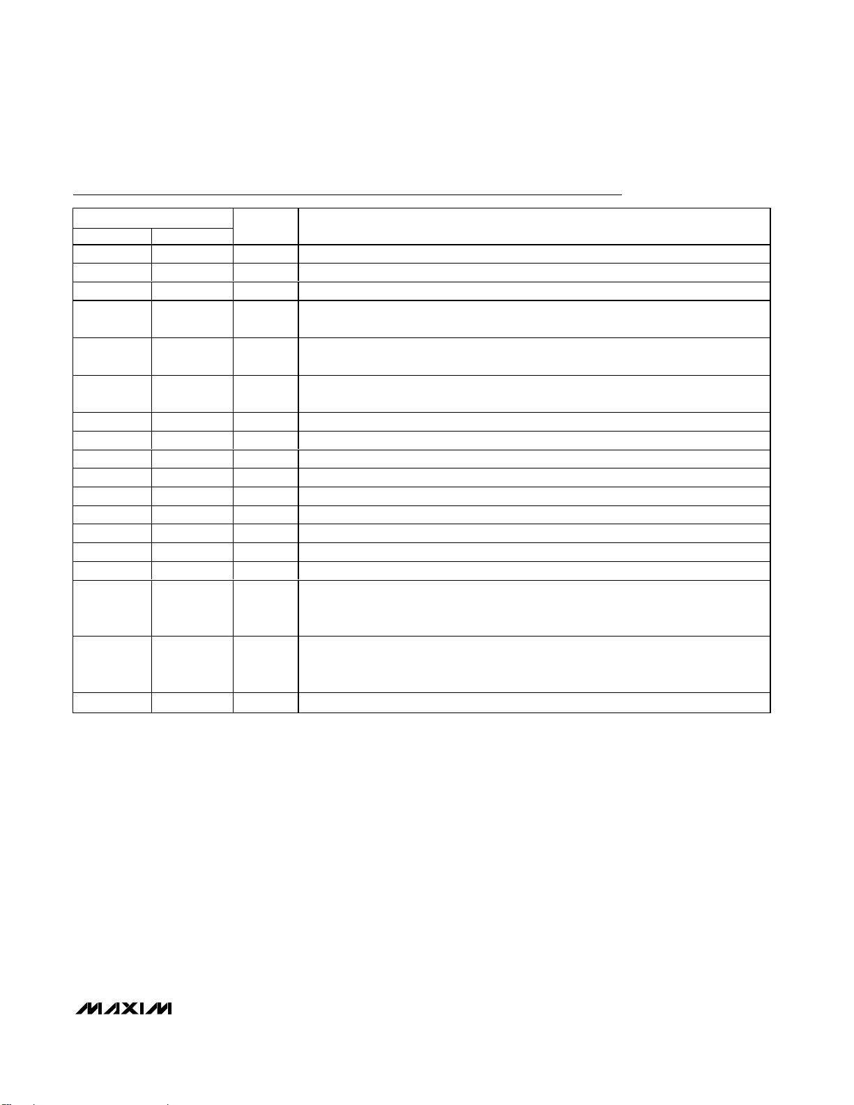
Ordering Information/Selector Guide
Note: All devices are specified over the -40°C to +85°C operating temperature range.
+Denotes lead-free package.
*EP = Exposed paddle.
TIME (ns)
NOTE: UI = 2.08ns
MASK = USB 2.0 HIGH SPEED
2.01.81.4 1.60.4 0.6 0.8 1.0 1.20.2
-0.4
-0.3
-0.2
-0.1
0
0.1
0.2
0.3
0.4
0.5
-0.5
0
COM
A
+ AND COM
A
- (V)
Eye Diagram
Pin Configurations appear at end of data sheet.
MAX4899EETE+ 16 TQFN-EP* DUAL 3:1 AEY T1633-4
MAX4899AEETE+ 16 TQFN-EP* DUAL 4:1 AEZ T1633-4
PART PIN-PACKAGE MUX CONFIGURATION TOP MARK PKG CODE
Page 2
MAX4899E/MAX4899AE
USB 2.0 High-Speed, Fault-Tolerant 3:1, 4:1
Multiplexers
2 _______________________________________________________________________________________
ABSOLUTE MAXIMUM RATINGS
Stresses beyond those listed under “Absolute Maximum Ratings” may cause permanent damage to the device. These are stress ratings only, and functional
operation of the device at these or any other conditions beyond those indicated in the operational sections of the specifications is not implied. Exposure to
absolute maximum rating conditions for extended periods may affect device reliability.
(All Voltages Referenced to GND.)
V+ .............................................................................-0.3V to +4V
QP, EN, C
0
, C1, (Note 1) ..........................................-0.3V to +4V
COM
A+
, COMA_, USB0+, USB0-, USB1+, USB1-, USB2+,
USB2-, USB3+, USB3- ......................................-0.3V to +5.5V
Continuous Current (COM
A
_ to USB_)...........................±120mA
Peak Current (COM
A
_ to USB_)
(pulsed at 1ms, 10% duty cycle).................................±240mA
Continuous Power Dissipation (T
A
= +70°C)
16-Pin TQFN (derate 20.8mW/°C above +70°C) ........1667mW
Operating Temperature Range ...........................-40°C to +85°C
Storage Temperature Range .............................-65°C to +150°C
Junction Temperature......................................................+150°C
Lead Temperature (soldering, 10s) .................................+300°C
ELECTRICAL CHARACTERISTICS
(V+ = +2.7V to +3.6V, TA= -40°C to +85°C, QP = low, EN = low, unless otherwise noted. Typical values are at V+ = +3.3V and TA=
+25°C.) (Note 2)
)
Note 1: Signals exceeding GND are clamped by internal diodes. Limit forward-diode current to maximum current rating.
ANALOG SWITCH (COMA_, USB__)
On-Resistance R
On-Resistance Match Between
Channels
On-Resistance Flatness R
Off-Leakage Current I
On-Leakage Current I
Quiescent Supply Current I+
Fault-Protection Trip Threshold V
ESD PROTECTION
COMA+, COMA- Human Body Model ±15 kV
PARAMETER SYMBOL CONDITIONS MIN TYP MAX UNITS
ON
ΔR
ON
FLAT (ON
L(OFF)
L(ON)
FP
V+ = 2.7V, I
-10mA, V
COMA_
1.5V, QP = low
V+ = 2.7V, I
-10mA, V
COM_
1.5V, 2.7V, QP = low
V+ = 2.7V, I
-10mA, V
COMA_
1.5V, QP = high
V+ = 3.0V, I
-10mA, V
COMA_
1.5V, QP = high
V+ = 2.7V, I
-10mA, V
COMA_
1.5V, 2.7V
V+ = 2.7V, I
1.5V, 2.7V
V+ = 3.6V, V
V+ = 3.6V, V
V+ = 3.6V, C
0 or V+
V+ = 3.3V 3.6 3.9 4.2 V
COMA_
= 0V,
COMA_
= 0V,
COMA_
= 0V,
COMA_
= 0V,
COMA_
= 0V,
COMA_
COMA_
COMA_
= C1 =
0
=
TA = +25°C 4 5
T
= -40°C to +85°C 6
A
=
TA = +25°C 4 7
= -40°C to +85°C 8
T
A
=
TA = +25°C 8 17
T
= -40°C to +85°C 18
A
=
TA = +25°C 4 12
T
= -40°C to +85°C 13
A
=
TA = +25°C 0.5 0.8
= -40°C to +85°C 1.0
T
A
= -10mA, V
= V
USB__
= V
USB__
= 0V,
COMA_
= 0.3V, 3.3V -1 +1 µA
= 0.3V, 3.3V -1 +1 µA
QP = low 250 600
QP = high 3
0.5 1.1 Ω
Ω
Ω
µA
Page 3
MAX4899E/MAX4899AE
USB 2.0 High-Speed, Fault-Tolerant 3:1, 4:1
Multiplexers
_______________________________________________________________________________________ 3
ELECTRICAL CHARACTERISTICS (continued)
(V+ = +2.7V to +3.6V, TA= -40°C to +85°C, QP = low, EN = low, unless otherwise noted. Typical values are at V+ = +3.3V and TA=
+25°C.) (Note 2)
Note 2: Limits at -40°C are guaranteed by design.
Note 3: Guaranteed by design.
Note 4: Charge-pump noise is specified as a peak-to-peak value.
SWITCH AC PERFORMANCE (Note 3)
On-Loss ON
Crosstalk
Off-Isolation V
Charge-Pump Noise V
Bandwidth -3dB BW RS = RL = unbalanced 50Ω 425 MHz
Off-Capacitance C
On-Capacitance C
Propagation Delay t
Output Skew Same Switch t
Fault-Protection Response Time t
Fault-Protection Recovery Time t
Charge Injection Q V
Enable Turn-On Time t
PARAMETER SYMBOL CONDITIONS MIN TYP MAX UNITS
f = 10MHz, 0 < VIN < 1V, Figure 1 0.5 dB
,
f = 50MHz, Figure 1 -50 dB
f = 50MHz, Figure 1 -45 dB
COMA_, USB_, RL = RS = 50Ω (Note 4) 100 µV
QP
f = 1MHz, COMA_, USB_, Figure 2 10.5 pF
f = 1MHz, COMA_, USB_, Figure 2 15 pF
ON
RL = RS = 50Ω, Figure 3 200 ps
Skew between opposite transitions in same
switch, Figure 3
V
50Ω, C
V
50Ω, C
V
= 0V to 5V to V
COMA_
= 10pF, Figure 4
L
= 5V to 3V to V
COMA_
= 10pF, Figure 4
L
= 0, CL = 1000pF, Figure 5 25 pC
GEN
= V + , RL = 50Ω , C L = 10p F, Fi g ur e 6 2.8 µs
U S B 0+
USB__
USB__
= 2.5V, RL =
= 1.5V, RL =
100 ps
1µs
1µs
V
V
LOSS
CT1
DCT1
ISO
OFF
PD
SK
FP
FPR
ON
Enable Turn-Off Time t
Address Transition Time t
Total Harmonic Distortion Plus
Noise
SWITCH LOGIC (QP, EN, C0, C1)
Logic-Input Voltage Low V
Logic-Input Voltage High V
Input Logic Hysteresis V
Input Leakage Current I
TRANS
THD+N
OFF
HYST
LEAK
V
= V + , RL = 50Ω , C L = 10p F, Fi g ur e 6 3 ns
U S B 0+
V
= V + , RL = 50Ω , C L = 10p F, Fi g ur e 7 1.2 µs
U S B 0+
f = 20Hz to 20kHz, V
600Ω
IL
IH
V+ = 3.6V, C0 = 0 or V+, C1 = 0 or V+ -1 1 µA
COMA_
= 1V
P-P
, RL =
0.02 %
0.4 V
1.4 V
100 mV
Page 4
MAX4899E/MAX4899AE
USB 2.0 High-Speed, Fault-Tolerant 3:1, 4:1
Multiplexers
4 _______________________________________________________________________________________
Typical Operating Characteristics
(V+ = 3.3V, QP = EN = low, TA= +25°C, unless otherwise noted.)
2.80
2.86
2.84
2.82
2.88
2.90
2.92
2.94
2.96
2.98
3.00
01.20.6 1.8 2.4 3.0 3.6
ON-RESISTANCE vs. V
COM
MAX4899E toc01
V
COM
(V)
R
ON
(Ω)
V+ = 2.7V
V+ = 3.3V
V+ = 3.6V
2.0
2.2
2.4
2.6
2.8
3.0
3.2
3.4
3.6
0 1.1 2.2 3.3
ON-RESISTANCE vs. V
COM
MAX4899E toc02
V
COM
(V)
R
ON
(Ω)
TA = +85°C
TA = +25°C
TA = -40°C
1500
1000
500
0
-500
3000
2500
2000
3500
4000
5000
4500
5500
-40 -15 10 35 60 85
LEAKAGE CURRENT vs. TEMPERATURE
MAX4899E toc03
TEMPERATURE (°C)
LEAKAGE CURRENT (pA)
COM 0N-LEAKAGE
COM 0FF-LEAKAGE
V+ = 3.6V
0
10
5
20
15
25
30
0 1.1 2.2 3.3
CHARGE INJECTION vs. V
COM
MAX4899E toc04
V
COM
(V)
CHARGE INJECTION (pC)
CL = 1000pF
100
160
140
120
180
200
220
240
260
280
300
-40 10-15 35 60 85
QUIESCENT SUPPLY CURRENT
vs. TEMPERATURE
MAX4899E toc05
TEMPERATURE (°C)
QUIESCENT SUPPLY CURRENT (μA)
V+ = 2.7V
V+ = 3.6V
V+ = 3.3V
0
0.3
0.2
0.1
0.4
0.5
0.6
0.7
0.8
0.9
1.0
2.7 3.0
3.3
3.6
LOGIC THRESHOLD vs. SUPPLY VOLTAGE
MAX4899E toc06
SUPPLY VOLTAGE (V)
LOGIC THRESHOLD (V)
V
IH
V
IL
FREQUENCY RESPONSE
MAX4899E toc07
FREQUENCY (MHz)
LOSS (dB)
10010
-90
-80
-70
-60
-50
-40
-30
-20
-10
0
-100
11000
ON-RESPONSE
OFF-ISOLATION
CROSSTALK
TOTAL HARMONIC DISTORTION
PLUS NOISE vs. FREQUENCY
MAX4899E toc08
FREQUENCY (Hz)
THD+N (%)
10k1k10010 100k
0.1
0.01
RL = 600
Ω
EYE DIAGRAM
TIME (ns)
2.01.81.4 1.60.4 0.6 0.8 1.0 1.20.2
-0.4
-0.3
-0.2
-0.1
0
0.1
0.2
0.3
0.4
0.5
-0.5
0
COM
A
+ AND COM
A
- (V)
MAX4899E toc09
Page 5
MAX4899E/MAX4899AE
USB 2.0 High-Speed, Fault-Tolerant 3:1, 4:1
Multiplexers
_______________________________________________________________________________________ 5
Pin Description
PIN
MAX4899E MAX4899AE
1 1 GND Ground
2 2 COMA+ Analog Switch Common D+ Terminal
3 3 COMA- Analog Switch Common D- Terminal
44V+
55C
66C
7, 8 — N.C. No Connection. Not internally connected.
— 7 USB3- Analog Switch 3 D- Terminal
— 8 USB3+ Analog Switch 3 D+ Terminal
9 9 USB2- Analog Switch 2 D- Terminal
10 10 USB2+ Analog Switch 2 D+ Terminal
11 11 USB1+ Analog Switch 1 D+ Terminal
12 12 USB1- Analog Switch 1 D- Terminal
13 13 USB0+ Analog Switch 0 D+ Terminal
14 14 USB0- Analog Switch 0 D- Terminal
15 15 EN
NAME FUNCTION
Positive Supply-Voltage Input. Connect V+ to a 2.7V to 3.6V supply voltage. Bypass V+
to GND with a 0.1µF capacitor placed as close as possible to the device.
Digital Control Input 1. C1 and C0 control the analog signal path as shown in the
1
Functional Diagrams section.
Digital Control Input 0. C1 and C0 control the analog signal path as shown in the
0
Functional Diagrams section.
Active-Low Enable Input. For normal operation, drive EN low. Drive EN high to place all
channels in a high-impedance state. The internal charge pump is turned off when EN is
a logic-high.
Active-Low Charge-Pump Enable Input. Drive QP low for normal operation. Drive QP
16 16 QP
— — EP Exposed Paddle. Connect EP to GND.
high to disable the charge pump with the switches still active at a reduced analog signal
range and higher R
ON
.
Page 6

MAX4899E/MAX4899AE
USB 2.0 High-Speed, Fault-Tolerant 3:1, 4:1
Multiplexers
6 _______________________________________________________________________________________
Test Circuits/Timing Diagrams
Figure 1. Off-Isolation, On-Loss, and Crosstalk
Figure 2. Channel Off-/On-Capacitance
0.1μF
V+
NETWORK
V
IN
CHANNEL
SELECT
C
C
0
1
V+
MAX4899E
USB_
MAX4899AE
QP
EN
MEASUREMENTS ARE STANDARDIZED AGAINST SHORT AT SOCKET TERMINALS.
OFF-ISOLATION IS MEASURED BETWEEN COM_ AND "OFF" USB_ TERMINAL ON EACH SWITCH.
ON-LOSS IS MEASURED BETWEEN COM_ AND "ON" USB_ TERMINAL ON EACH SWITCH.
CROSSTALK IS MEASURED FROM ONE USB_ CHANNEL TO ANOTHER USB_ CHANNEL.
SIGNAL DIRECTION THROUGH SWITCH IS REVERSED; WORST VALUES ARE RECORDED.
COM_
GND
V
OUT
50Ω
MEAS.
ANALYZER
50Ω
50Ω 50Ω
OFF-ISOLATION = 20log
ON-LOSS = 20log
REF.
CROSSTALK = 20log
V
OUT
V
IN
V
OUT
V
IN
V
OUT
V
IN
CHANNEL
SELECT
C
0
C
1
QP
EN
V+
V+
MAX4899E
MAX4899AE
GND
USB_,
COM_
1MHz
CAPACITANCE
ANALYZER
Page 7

MAX4899E/MAX4899AE
USB 2.0 High-Speed, Fault-Tolerant 3:1, 4:1
Multiplexers
_______________________________________________________________________________________ 7
Test Circuits/Timing Diagrams (continued)
Figure 3. Propagation Delay and Output Skew
MAX4899E
50%
MAX4899AE
C0C
1
COM
COM
A+
A-
50%
OUT+
RISE-TIME PROPAGATION DELAY = t
R
L
R
L
FALL-TIME PROPAGATION DELAY = t
tSK = |t
PLHX
OUT-
t
INRISE
90%
10% 10%
OR t
OR t
PLHY
PHLY
.
.
PLHX
- t
| OR |t
PHLX
PHLY
90%
- t
t
INFALL
PLHY
PHLX
|.
R
S
IN+
IN-
V+
V
IN+
0V
USB_+
R
S
USB_-
V+
V
V
V
OUT+
OUT-
IN-
0V
t
PLHX
V+
0V
V+
0V
t
PHLY
50%
50%
50%
t
PHLX
t
PLHY
50%
50%
50%
t
OUTRISE
90%
10% 10%
90%
t
OUTFALL
Page 8

MAX4899E/MAX4899AE
USB 2.0 High-Speed, Fault-Tolerant 3:1, 4:1
Multiplexers
8 _______________________________________________________________________________________
Figure 4. Fault-Protection Response/Recovery Time
Test Circuits/Timing Diagrams (continued)
Figure 5. Charge Injection
5V
2.5V
COM
A-
t
FP
t
FP
2.5V
USB_
V+
V
CO
C
C
EN
QP
0
1
V+
MAX4899E
MAX4899AE
GND
USB0_
COM
V
CL
1000pF
_
A
V
GEN
OUT
3V
0V
t
FPR
3V
1.5V
0V
V+
V
CO
0
V
OUT
Δ V
OUT
Δ V
IS THE MEASURED VOLTAGE DUE TO CHARGE-
OUT
REPEAT TEST FOR EACH SECTION.
TRANSFER ERROR Q WHEN THE CHANNEL TURNS OFF.
Q = Δ V
X CL.
OUT
Page 9

MAX4899E/MAX4899AE
USB 2.0 High-Speed, Fault-Tolerant 3:1, 4:1
Multiplexers
_______________________________________________________________________________________ 9
Figure 6. Enable Switching Times
Figure 7. Address Transition Time
Test Circuits/Timing Diagrams (continued)
C
0
C
1
MAX4899E
MAX4899AE
V
EN
EN
QP
V
ADD
C
0
C
1
MAX4899E
MAX4899AE
EN
QP
GND
V+
V+
GND
V+
V+
USB0+
COM
USB0+
USB1+
USB2+
USB3+
COM
USB1+
USB2+
USB3+
+
A
V+
V
EN
0
V
OUT
10pF
10pF
V
OUT
0
t
OFF
ADD
V+
0
V
OUT
0
t
TRANS
V
V
OUT
+
A
50Ω
50Ω
50%
50%
90%
90%
90%
90%
t
TRANS
t
ON
Page 10

MAX4899E/MAX4899AE
USB 2.0 High-Speed, Fault-Tolerant 3:1, 4:1
Multiplexers
10 ______________________________________________________________________________________
Detailed Description
The MAX4899E/MAX4899AE analog multiplexers combine the low on-capacitance (CON) and low on-resistance (R
ON
) necessary for high-performance switching
applications. These devices are designed for USB 2.0
high-speed applications at 480Mbps. The MAX4899E/
MAX4899AE also handle all the requirements for USB
low- and full-speed signaling. In the case of USB low/
full speed, these devices can function normally even if
the supply voltage is 2.7V, even though the USB signal
may be higher than the supply voltage.
The MAX4899E is a dual 3:1 multiplexer, whereas the
MAX4899AE is a dual 4:1 multiplexer. The MAX4899E/
MAX4899AE feature two digital inputs, C
0
and C1, to control the analog signal path. Typical applications include
switching a USB connector between USB and other operations such as serial communications, audio, and video.
An enable input (EN) is provided to disable all channels
and place the device into a high-impedance (off) state,
as well as shutting off the charge pump for minimum
power consumption. The MAX4899E/MAX4899AE feature an additional charge-pump enable input (QP) to
disable the charge pump. The switches remain active
at a lower analog signal range and higher RON.
The MAX4899E/MAX4899AE operate from a 2.7V to
3.6V power-supply voltage and are current-limit protected against +5.5V shorts to COMA- and COMA+.
Digital Control Inputs (C0, C1)
The MAX4899E/MAX4899AE provide two digital control
inputs (C0, C1) to select the analog signal path
between the COMA_ and USB__ channels. The truth
tables for the MAX4899E/MAX4899AE are shown in the
Functional Diagrams. Since the MAX4899E only has
three USB__ channels, the code C1:C0= 1:1 can be
used to place all channels into a high-impedance state.
This is particularly useful for eliminating the extra control line to the EN input that is normally used for disabling all channels. Driving C0and C1rail-to-rail
minimizes power consumption.
Enable Input (EN)
The MAX4899E/MAX4899AE feature an enable input
(EN) that when driven high places all channels into a
high-impedance state, as an all-off feature. The internal
charge pump is also disabled when EN is high, thus
minimizing the quiescent supply current. For normal
operation, drive EN low.
Charge-Pump Enable Input (QP)
The charge-pump input (QP) disables and enables the
internal charge pump. Drive QP high to disable the
charge pump and reduce the quiescent supply current.
With the charge pump disabled, the MAX4899E/
MAX4899AE still function normally; however, the analog
signal range is reduced and the switch on-resistance
(R
ON
) is increased. The analog signal range with the
charge pump disabled is 0V to 1.5V. For normal operation, drive QP low.
Analog Signal Levels
Signals applied to COMA+ are routed to the USB_+ terminals, and signals applied to COMA- are routed to the
USB_- terminals. These multiplexers are bidirectional,
allowing COMA_ and USB_ to be configured as either
inputs or outputs. The D+ and D- notation in the Pin
Description table is arbitrary and can be interchanged.
For example, USB D+ signals can be applied to COMAand are routed to the USB_- terminals. Additionally,
these multiplexers can be used for non-USB signals.
COMA+ and COMA- are normally connected to outside
circuitry and are ±15kV ESD protected.
The MAX4899E is a dual 3:1 multiplexer, allowing
COMA+ to be routed to one of three USB_+ channels,
and COMA- to be routed to one of three USB_- channels.
The MAX4899AE is a dual 4:1 multiplexer, allowing
COMA+ to be routed to one of four USB_+ channels, and
COMA- to be routed to one of four USB_- channels.
Overvoltage Fault Protection
The MAX4899E/MAX4899AE feature +5.5V fault protection to COMA+ and COMA-. When a fault occurs
between 4.5V to 5.5V, the switch automatically goes
into a current-limiting mode that limits current to less
than 2mA. Fault protection prevents these switches and
downstream devices from being damaged due to
shorts to the USB bus voltage rail.
Applications Information
USB Switching
The MAX4899E/MAX4899AE analog multiplexers are
fully compliant with the USB 2.0 specification. The low
on-resistance and low on-capacitance of these multiplexers make them ideal for high-performance switching applications. The MAX4899E/MAX4899AE are ideal
for routing USB data lines and for applications that
require switching between different data types (see
Figure 8).
Board Layout
High-speed switches require proper layout and design
procedures for optimum performance. Keep designcontrolled impedance PC board traces as short as possible. Ensure that bypass capacitors are placed as
close to the device as possible and use large ground
planes where possible.
Page 11

MAX4899E/MAX4899AE
USB 2.0 High-Speed, Fault-Tolerant 3:1, 4:1
Multiplexers
______________________________________________________________________________________ 11
ESD Protection
As with all Maxim devices, ESD-protection structures are
incorporated on all pins to protect against electrostatic
discharges encountered during handling and assembly.
The COM
A
+ and COMA- lines have extra protection
against static electricity. Maxim’s engineers have developed state-of-the-art structures to protect these pins
against ESD of ±15kV without damage. The ESD structures withstand high ESD in all states: normal operation,
tri-state output mode, and powered down. After an ESD
event, Maxim’s E-versions keep working without latchup, whereas competing products can latch and must be
powered down to remove latch-up.
Human Body Model
The MAX4899E/MAX4899AE COM
A
+ and COMA- pins
are characterized for ±15kV ESD protection using the
Human Body Model (MIL-STD-883, Method 3015).
Figure 9a shows the Human Body Model and Figure 9b
shows the current waveform it generates when discharged into a low impedance. This model consists of
a 100pF capacitor charged to the ESD voltage of interest, which is then discharged into the device through a
1.5kΩ resistor.
Figure 8. MAX4899AE Multiplexing Four Data Types
Figure 9a. Human Body ESD Test Model
Figure 9b. Human Body Model Current Waveform
Chip Information
PROCESS: BiCMOS
USB
TRANSCEIVER
USB
CONNECTOR
V
BUS
D+
D-
GND
USB0+
COMA+
COM
-
A
USB3+ USB3-
SERIAL DATA LINK
MAX4899AE
USB0-
USB1+
USB1-
USB2+
USB2-
AUDIO
HEADPHONE
AUXILIARY
INPUT
1MΩ RD 1500Ω
R
C
DISCHARGE
RESISTANCE
STORAGE
CAPACITOR
HIGH-
VOLTAGE
DC
SOURCE
CHARGE-CURRENT-
LIMIT RESISTOR
C
s
100pF
DEVICE
UNDER
TEST
PEAK-TO-PEAK RINGING
I
r
(NOT DRAWN TO SCALE)
AMPERES
IP 100%
90%
36.8%
10%
0
0
t
RL
TIME
t
DL
CURRENT WAVEFORM
Page 12

MAX4899E/MAX4899AE
USB 2.0 High-Speed, Fault-Tolerant 3:1, 4:1
Multiplexers
12 ______________________________________________________________________________________
Functional Diagrams
X = 1 or 0.
V+ V+
MAX4899E
COMA+
COM
-
A
EN
C
0
C
1
QP EN C
0000
0001
0010
0 0 1 1 HIGH-Z ALL OFF
0 1 X X HIGH-Z ALL OFF
1 1 X X HIGH-Z ALL OFF
1000
1001
1010
1 0 1 1 HIGH-Z ALL OFF
CONTROL
1C0
LOGIC
GND
MAX4899E
FUNCTION COMMENT
COM
+ →USB0+
A
- →USB0-
COM
A
COM
+ →USB1+
A
- →USB1-
COM
A
COM
+ →USB2+
A
- →USB2-
COM
A
COM
+ →USB0+
A
- →USB0-
COM
A
COM
+ →USB1+
A
- →USB1-
COM
A
COM
+ →USB2+
A
- →USB2-
COM
A
CHARGE
PUMP
NORMAL
OPERATION
NORMAL
OPERATION
NORMAL
OPERATION
LARGER R
LARGER R
LARGER R
USB0+
USB0-
USB1+
USB1-
USB2+
USB2-
QP
ON
ON
ON
MAX4899AE
COM
+
A
-
COM
A
EN
C
0
C
1
QP EN C
0000
0001
0010
0011
0 1 X X HIGH-Z ALL OFF
1 1 X X HIGH-Z ALL OFF
1000
1001
1010
1011
CONTROL
LOGIC
1C0
GND
MAX4899AE
FUNCTION COMMENT
COMA+ →USB0+
COMA- →USB0-
COMA+ →USB1+
COMA- →USB1-
COMA+ →USB2+
COMA- →USB2-
COMA+ →USB3+
COMA- →USB3-
COMA+ →USB0+
COMA- →USB0-
COMA+ →USB1+
COMA- →USB1-
COMA+ →USB2+
COMA- →USB2-
COMA+ →USB3+
COMA- →USB3-
CHARGE
PUMP
NORMAL
OPERATION
NORMAL
OPERATION
NORMAL
OPERATION
NORMAL
OPERATION
LARGER R
LARGER R
LARGER R
LARGER R
USB0+
USB0-
USB1+
USB1-
USB2+
USB2-
USB3+
USB3-
QP
ON
ON
ON
ON
Page 13

MAX4899E/MAX4899AE
USB 2.0 High-Speed, Fault-Tolerant 3:1, 4:1
Multiplexers
______________________________________________________________________________________ 13
Pin Configurations
TOP VIEW
USB0+
USB0-
TOP VIEW
USB2+
-
A
COM
4
USB2-
V+
USB3+
8
USB3-
7
C
6
0
C
5
1
USB2+
-
A
COM
4
USB2-
V+
N.C.
8
N.C.
7
C
6
0
C
5
1
USB0+
USB0-
EN
QP
USB1-
12 10 9
11
13
*EP
14
15
EN
16
QP
MAX4899E
+
13
2
+ USB1+
A
GND
COM
TQFN
*CONNECT EXPOSED PAD TO GND
USB1-
12 10 9
11
13
*EP
14
15
16
MAX4899AE
+
13
2
+ USB1+
A
GND
COM
TQFN
Page 14

MAX4899E/MAX4899AE
USB 2.0 High-Speed, Fault-Tolerant 3:1, 4:1
Multiplexers
Maxim cannot assume responsibility for use of any circuitry other than circuitry entirely embodied in a Maxim product. No circuit patent licenses are
implied. Maxim reserves the right to change the circuitry and specifications without notice at any time.
14 ____________________Maxim Integrated Products, 120 San Gabriel Drive, Sunnyvale, CA 94086 408-737-7600
© 2006 Maxim Integrated Products is a registered trademark of Maxim Integrated Products, Inc.
Boblet
Package Information
(The package drawing(s) in this data sheet may not reflect the most current specifications. For the latest package outline information,
go to www.maxim-ic.com/packages
.)
MARKING
D
E
E/2
D/2
AAAA
C
L
(ND - 1) X e
(NE - 1) X e
D2/2
e
D2
12x16L QFN THIN.EPS
C
L
0.10 C 0.08 C
A
A2
A1
8L 3x3
PKG
REF. MIN.
MIN.
NOM. MAX.
0.70 0.75 0.80
A
b
0.25 0.30 0.35
D
2.90
3.00 3.10
E
2.90 3.00 3.10
e
0.65 BSC.
L
0.35
0.55 0.75
ND
NE
0
0.02
A1
A2
0.20 REF
0.25
k
12L 3x3
NOM. MAX. NOM.
0.70
0.75
0.20
0.25
2.90
3.00
2.90
3.00
0.50 BSC.
0.45
8
2
2
-
0.55
0.05
0.0230.05
0
0.20 REF
-
0.25
12N
3
-
0.80
0.30
3.10
3.10
0.65
-
16L 3x3
MIN. MAX.
0.70
0.75
0.20
0.25
2.90
3.00
2.90
3.00
0.50 BSC.
0.30
0.40
16
4
040.02
0.20 REF
-
0.25
0.80
0.30
3.10
3.10
0.50
0.05
-
k
C
L
L
e
EXPOSED PAD VARIATIONS
PKG.
CODES
TQ833-1 1.250.25 0.70 0.35 x 45° WEEC1.250.700.25
T1233-1
T1233-3
T1233-4
T1633-2 0.95
T1633F-3
T1633FH-3 0.65 0.80 0.95
T1633-4 0.95
T1633-5 0.95
D2
MIN.
NOM.
0.95
1.10
1.10
0.95
1.10
0.65
0.80
1.10 1.25 0.95 1.10
1.10
MAX.
1.25
1.25
1.251.10
1.25
0.95
1.25
E2/2
L
E2
PACKAGE OUTLINE
8, 12, 16L THIN QFN, 3x3x0.8mm
E2
NOM.
MIN.
MAX.
1.10
0.95
1.25
0.95 1.10 0.35 x 45°1.25 WEED-10.95
1.100.95
1.10
1.25
0.95
0.80
0.95
0.65
0.95
0.65 0.80
1.25
1.10 1.25
e
PIN ID
0.35 x 45°
0.35 x 45°
0.35 x 45°
0.225 x 45°
0.225 x 45°
0.35 x 45°
0.35 x 45° WEED-20.95
b
C
L
21-0136
0.10 M C A B
JEDEC
WEED-1
WEED-11.25
WEED-2
WEED-2
WEED-2
WEED-2
L
1
I
2
NOTES:
1. DIMENSIONING & TOLERANCING CONFORM TO ASME Y14.5M-1994.
2. ALL DIMENSIONS ARE IN MILLIMETERS. ANGLES ARE IN DEGREES.
3. N IS THE TOTAL NUMBER OF T ERMINALS.
4. THE TERMINAL #1 IDENTIFIER AND TERMINAL NUMBERING CONVENTION SHALL CONFORM TO
JESD 95-1 SPP-012. DETAILS OF TERMINAL #1 IDENTIFIER ARE OPTIONAL, BUT MUST BE LOCATED
WITHIN THE ZONE INDICATED. THE TERMINAL #1 IDENTIFIER MAY BE EITHER A MOLD OR
MARKED FEATURE.
5. DIMENSION b APPLIES TO METALLIZED TERMINAL AND IS MEASURED BETWEEN 0.20 mm AND 0.25 mm
FROM TERMINAL TIP.
6. ND AND NE REFER TO THE NUMBER OF TERMINALS ON EACH D AND E SIDE RESPECTIVELY.
7. DEPOPULATION IS POSSIBLE IN A SYMMETRICAL FASHION.
8. COPLANARITY APPLIES TO THE EXPOSED HEAT SINK SLUG AS WELL AS THE TERMINALS .
9. DRAWING CONFORMS TO JEDEC MO220 REVISION C.
10. MARKING IS FOR PACKAGE ORIENTATION REFERENCE ONLY.
11. NUMBER OF LEADS SHOWN ARE FOR REFERENCE ONLY.
12. WARPAGE NOT TO EXCEED 0.10mm.
PACKAGE OUTLINE
8, 12, 16L THIN QFN, 3x3x0.8mm
21-0136
2
I
2
 Loading...