

Page 1
现货库存、技术资料、百科信息、热点资讯,精彩尽在鼎好!
General Description
The MAX4890E/MAX4892E meet the needs of high-speed
differential switching. The devices handle the needs of
Gigabit Ethernet (10/100/1000) Base-T switching as
well as LVDS and LVPECL switching. The MAX4890E/
MAX4892E provide enhanced ESD protection up to
±15kV, and excellent high-frequency response, making
the devices especially useful for interfaces that must go to
an outside connection.
Both devices provide extremely low capacitance
(CON), as well as low resistance (RON), for low-insertion
loss and very wide bandwidth. In addition to the four
pairs of DPDT switches, the MAX4892E provides LED
switching for laptop computer/docking station use.
The MAX4890E/MAX4892E are pin-for-pin equivalents
to the MAX4890/MAX4892 and can replace these
devices for those applications requiring the enhanced
ESD protection. Both devices are available in spacesaving TQFN packages and operate over the standard
-40°C to +85°C temperature range.
Applications
Notebooks and Docking Stations
Servers and Routers with Ethernet Interfaces
Board-Level Redundancy Protection
SONET/SDH Signal Routing
T3/E3 Redundancy Protection
LVDS and LVPECL Switching
Features
♦ ±15kV ESD Protected Per MIL-STD-883, Method
3015
♦ Single +3.0V to +3.6V Power-Supply Voltage
♦ Low On-Resistance (RON): 4Ω (typ), 6.5Ω (max)
♦ Ultra-Low On-Capacitance (CON): 8pF (typ)
♦ -23dB Return Loss (100MHz)
♦ -3dB Bandwidth: 650MHz
♦ Optimized Pin Out for Easy Transformer and PHY
Interface
♦ Built-In LED Switches for Switching Indicators to
Docking Station (MAX4892E)
♦ Low 450µA (max) Quiescent Current
♦ Bidirectional 8 to 16 Multiplexer/Demultiplexer
♦ Standard Pin Out, Matching the MAX4890 and
MAX4892
♦ Space-Saving Lead-Free Packages
32-Pin, 5mm x 5mm, TQFN Package
36-Pin, 6mm x 6mm, TQFN Package
MAX4890E/MAX4892E
1000 Base-T, ±15kV ESD Protection LAN Switches
________________________________________________________________ Maxim Integrated Products 1
Ordering Information
19-0624; Rev 0; 8/06
For pricing, delivery, and ordering information, please contact Maxim/Dallas Direct! at
1-888-629-4642, or visit Maxim’s website at www.maxim-ic.com.
PART
PINPACKAGE
LED
PKG
CODE
MAX4890EETJ+
—
T-3255-4
MAX4892EETX+
3
T-3666-3
+Denotes lead-free package.
Note: All devices are specified over the -40°C to +85°C operating
temperature range.
*EP = Exposed pad.
Typical Operating Circuit and Functional Diagrams appear
at end of data sheet.
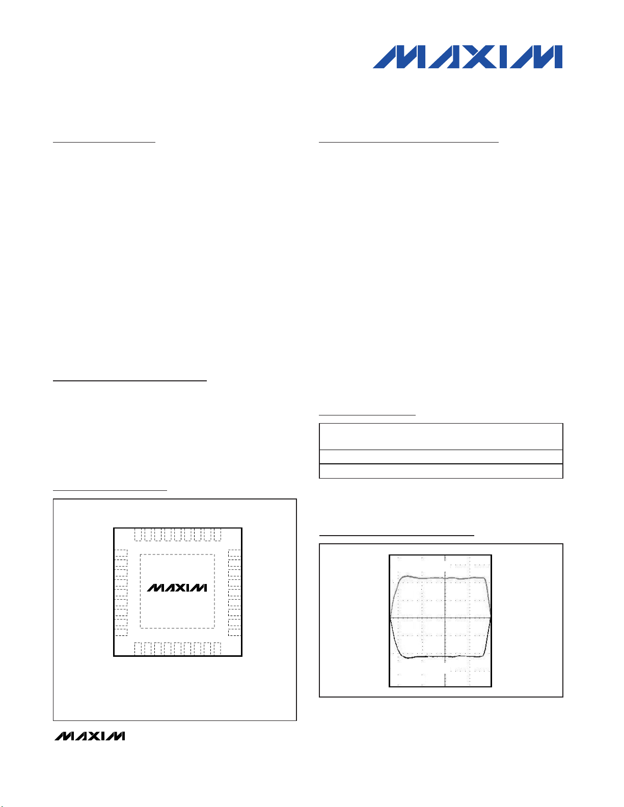
Eye Diagram
CH2: 4B2, 100mV/div
CH1: 5B2, 100mV/div
f = 125MHz
Pin Configurations
SEL
2B1
2B2
3B2
4B2
5B2
4B1
5B1
3B1
A3
LED0
0LED1
A4
A5
A6
A1
1
2
3
4
5
6
7
8
9
101112131415161718
363534333231302928
27
26
25
24
23
22
21
20
19
1LED2
7B2
6B2
6B1
1LED1
LED1
GND
A7
MAX4892E
TOP VIEW
0LED2
7B1
A2
A0
0B2
V+
LED2
2LED1
2LED2
0B1
1B1
1B2
TQFN
*EP
*EXPOSED PAD CONNECTED TO GND.
+
Pin Configurations continued at end of data sheet.
SWITCHES
32 TQFN-EP*
36 TQFN-EP*
Page 2
MAX4890E/MAX4892E
1000 Base-T, ±15kV ESD Protection LAN Switches
2 _______________________________________________________________________________________
ABSOLUTE MAXIMUM RATINGS
Stresses beyond those listed under “Absolute Maximum Ratings” may cause permanent damage to the device. These are stress ratings only, and functional
operation of the device at these or any other conditions beyond those indicated in the operational sections of the specifications is not implied. Exposure to
absolute maximum rating conditions for extended periods may affect device reliability.
V+ ……………………………………………………… -0.3V to +4V
All Other Pins………………………………….. -0.3V to (V+ + 0.3V)
Continuous Current (A_ to _B_) ......................................±120mA
Continuous Current (LED_ to _LED_) .…………………… ±40mA
Peak Current (A_ to _B_)
(pulsed at 1ms, 10% duty cycle) ……………………. ±240mA
Current into Any Other Pin................................................±20mA
Continuous Power Dissipation (T
A
= +70°C)
32-Pin TQFN (derate 34.5mW/°C above +70°C) …….. 2.76W
36-Pin TQFN (derate 35.7mW/°C above +70°C) …….. 2.85W
ESD Protection, Human Body Model .............................±15kV
Operating Temperature Range …………………. -40°C to +85°C
Junction Temperature.……………………………………. +150°C
Storage Temperature Range .…………………. -65°C to +150°C
Lead Temperature (soldering, 10s) .................................+300°C
ELECTRICAL CHARACTERISTICS
(V+ = +3V to +3.6V, TA= TJ= T
MIN
to T
MAX
, unless otherwise noted. Typical values are at V+ = 3.3V, TA= +25°C.) (Note 1)
PARAMETER
SYMBOL
CONDITIONS
MIN
TYP
MAX
UNITS
ANALOG SWITCH
TA = +25°C 4 5.5
On-Resistance R
ON
V+ = 3V,
I
A_
= -40mA,
V
A_
= 0, 1.5V, 3V
T
MIN
to T
MAX
6.5
Ω
On-Resistance LED Switches
(MAX4892E)
40 Ω
TA = +25°C 0.5 1.5
On-Resistance Match
Between Channels
∆R
ON
V+ = 3V,
I
A_
= -40mA,
V
A_
= 0, 1.5V, 3V
(Note 2)
T
MIN
to T
MAX
2
Ω
On-Resistance Flatness
)
V+ = 3V, IA_ = -40mA, V
A_
= 1.5V, 3V
Ω
Off-Leakage Current
)
V+ = 3.6V, VA_ = 0.3V, 3.3V;
V
_B1
or V
_B2
= 3.3V, 0.3V
-1 +1
On-Leakage Current
)
V+ = 3.6V, VA_= 0.3V, 3.3V;
V
_B1
or V
_B2
= 0.3V, 3.3V or floating
-1 +1
µA
ESD PROTECTION
ESD Protection
Human Body Model (spec MIL-STD-883,
Method 3015)
kV
SWITCH AC PERFORMANCE
Insertion Loss I
LOS
RS = RL = 50Ω, unbalanced, f = 1MHz,
(Note 2)
0.6 dB
Return Loss R
LOS
f = 100MHz -23 dB
R
ONLED
R
FLAT(ON
I
LA_(OFF
I
LA_(ON
V + = 3V , I
_L E D _
= - 40m A, V
= 0, 1.5V , 3V
LE D _
0.01
±15
Page 3
MAX4890E/MAX4892E
1000 Base-T ±15kV ESD Protection LAN Switch
_______________________________________________________________________________________ 3
ELECTRICAL CHARACTERISTICS (continued)
(V+ = +3V to +3.6V, TA= TJ= T
MIN
to T
MAX
, unless otherwise noted. Typical values are at V+ = 3.3V, TA= +25°C.) (Note 1)
PARAMETER
SYMBOL
CONDITIONS
MIN
TYP
MAX
UNITS
V
CT1
f = 25MHz -50
Crosstalk
V
CT2
Any switch to any
switch; R
S
= RL =
50Ω, unbalanced,
Figure 1
f = 125MHz -26
dB
SWITCH AC CHARACTERISTIC
-3dB Bandwidth BW RS = RL = 50Ω, unbalanced
MHz
Off-Capacitance C
OFF
f = 1MHz, _B_, A_ 3.5 pF
On-Capacitance C
ON
f = 1MHz, _B_, A_ 6.5 pF
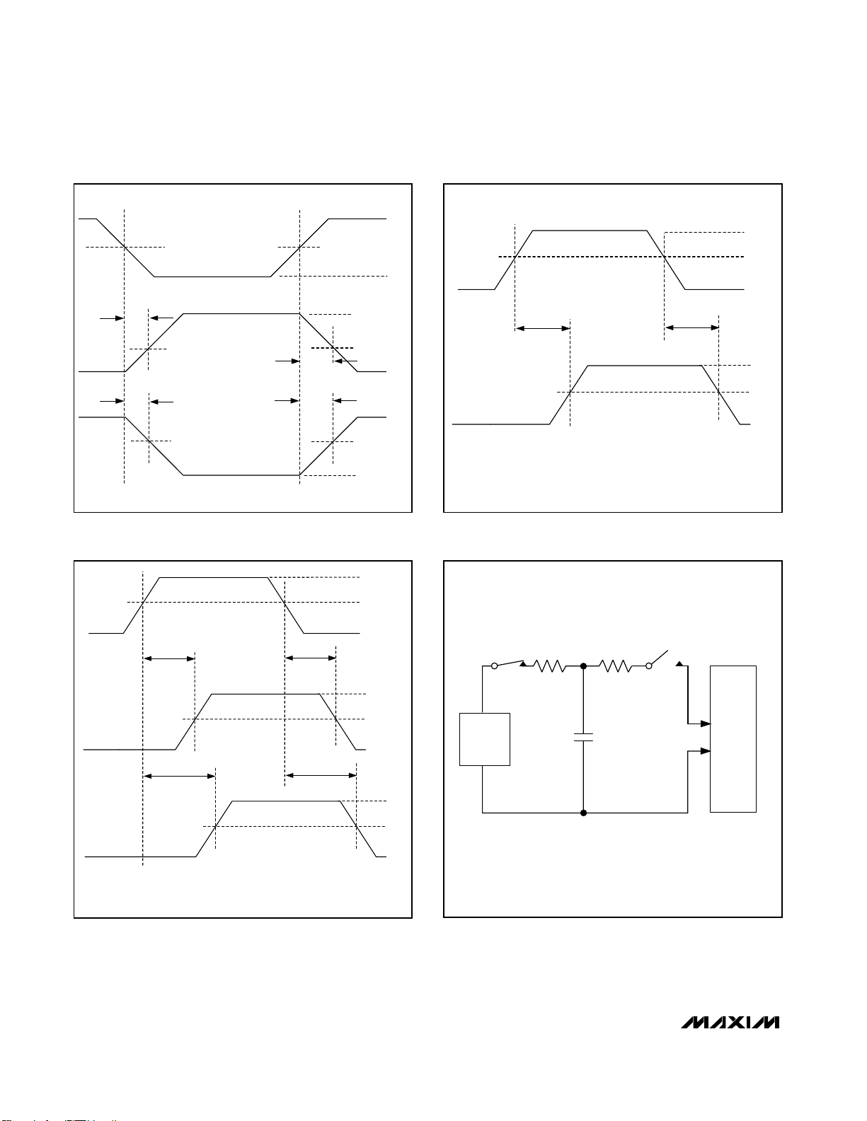
Turn-On Time t
ON
V
A_
= 1V, R
L
, 100Ω, Figure 2 50 ns
Turn-Off Time t
OFF
VA_ = 1V, RL, 100Ω, Figure 2 50 ns
Propagation Delay
RS = RL = 50Ω, unbalanced, Figure 3 0.1 ns
Output Skew Between Ports t
SK(o)
Skew between any two ports, Figure 4
ns
SWITCH LOGIC
Input-Voltage Low V
IL
V+ = 3.0V 0.8
Input-Voltage High V
IH
V+ = 3.6V 2.0
V
Input-Logic Hysteresis V
HYST
V+ = 3.3V
mV
Input Leakage Current I
SEL
V+ = 3.6V, V
SEL
= 0 or V+ -5 +5 µA
Operating Supply-Voltage Range
V+ 3.0 3.6 V
Quiescent Supply Current I+ V+ = 3.6V, V
SEL
= 0 or V+
µA
Note 1: Specifications at -40°C are guaranteed by design.
Note 2: Guaranteed by design.
t
PLH, tPHL
650
0.01
100
280 450
Page 4
MAX4890E/MAX4892E
1000 Base-T, ±15kV ESD Protection LAN Switches
4 _______________________________________________________________________________________
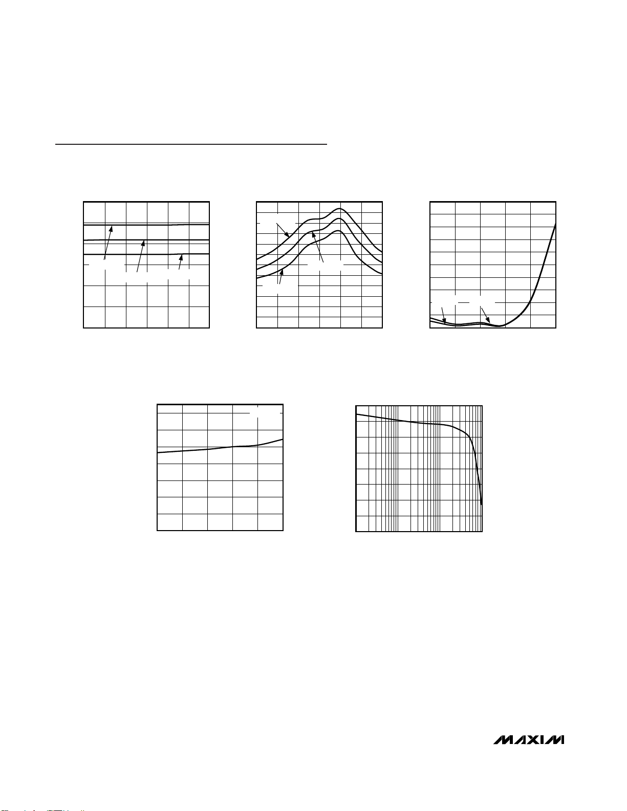
0
2
1
4
3
5
6
0 1.0 1.50.5 2.0 2.5 3.0
ON-RESISTANCE vs. V
A_
MAX4890E toc01
VA_ (V)
R
ON
(Ω)
TA = +85°C
TA = +25°C
TA = -40°C
0
8
10
12
14
6
2
4
16
18
22
20
24
01.0
0.5
1.5 2.0 2.5 3.0
LED_ON-RESISTANCE vs. V
LED_
MAX4890E toc02
V
LED_
(V)
R
ONLED
(Ω)
TA = +85°C
TA = +25°C
TA = -40°C
0
12
8
4
16
20
24
28
32
36
40
-40 10-15 35 60 85
LEAKAGE CURRENT vs. TEMPERATURE
MAX4890E toc03
TEMPERATURE (°C)
LEAKAGE CURRENT (pA)
ILA_(ON)
ILA_(OFF)
200
220
240
260
280
300
320
340
-40 -15 10 35 60 85
QUIESCENT SUPPLY CURRENT
vs. TEMPERATURE
MAX4890E toc04
TEMPERATURE (°C)
QUIESCENT SUPPLY CURRENT (µA)
V+ = 3.6V
SINGLE-ENDED INSERTION LOSS
vs. FREQUENCY
MAX4890E toc05
FREQUENCY (MHz)
INSERTION LOSS (dB)
10010
-7
-6
-5
-4
-3
-2
-1
0
-8
1 1000
Typical Operating Characteristics
(V+ = 3.3V, TA= +25°C, unless otherwise noted.)
Page 5

MAX4890E/MAX4892E
1000 Base-T ±15kV ESD Protection LAN Switch
_______________________________________________________________________________________ 5
Pin Description
PIN
MAX4892E
NAME FUNCTION
1 32 A1 Differential PHY Interface Pair. Connect to the Ethernet PHY.
2 1 A2 Differential PHY Interface Pair. Connect to the Ethernet PHY.
3 2 A3 Differential PHY Interface Pair. Connect to the Ethernet PHY.
4 — LED0 LED0 Input
5 — 0LED1 0LED1 Output. Drive SEL low (SEL = 0) to connect LED0 to 0LED1.
6 — 0LED2 0LED2 Output. Drive SEL high (SEL = 1) to connect LED0 to 0LED2.
7 7 A4 Differential PHY Interface Pair. Connect to the Ethernet PHY.
8 8 A5 Differential PHY Interface Pair. Connect to the Ethernet PHY.
9 9 A6 Differential PHY Interface Pair. Connect to the Ethernet PHY.
10 10 A7 Differential PHY Interface Pair. Connect to the Ethernet PHY.
11 11 GND Ground
12 — LED1 LED1 Input
13 — 1LED1 1LED1 Output. Drive SEL low (SEL = 0) to connect LED1 to 1LED1.
14 — 1LED2 1LED2 Output. Drive SEL high (SEL = 1) to connect LED1 to 1LED2.
15 13 7B2 B2 Differential Pair
16 14 6B2 B2 Differential Pair
17 15 7B1 B1 Differential Pair
18 16 6B1 B1 Differential Pair
19 17 5B2 B2 Differential Pair
20 18 4B2 B2 Differential Pair
21 19 5B1 B1 Differential Pair
22 20 4B1 B1 Differential Pair
23 21 3B2 B2 Differential Pair
24 22 2B2 B2 Differential Pair
25 23 3B1 B1 Differential Pair
26 24 2B1 B1 Differential Pair
27 29 SEL Select Input. SEL selects switch connection. See the Truth Table (Table1).
28 25 1B2 B2 Differential Pair
29 26 0B2 B2 Differential Pair
30 27 1B1 B1 Differential Pair
31 28 0B1 B1 Differential Pair
32 — 2LED2 2LED2 Output. Drive SEL high (SEL = 1) to connect LED2 to 2LED2.
33 — 2LED1 2LED1 Output. Drive SEL low (SEL = 0) to connect LED2 to 2LED1.
34 — LED2 LED2 Input
35 30 V+ Positive-Supply Voltage Input. Bypass to GND with a 0.1µF ceramic capacitor.
36 31 A0 Differential PHY Interface Pair. Connect to the Ethernet PHY.
— 3-6, 12 N.C. No Connection. Not internally connected.
——EP Exposed Pad. Connect exposed pad to GND or leave it unconnected.
MAX4890E
Page 6

MAX4890E/MAX4892E
1000 Base-T, ±15kV ESD Protection LAN Switches
6 _______________________________________________________________________________________
Detailed Description
The MAX4890E/MAX4892E are high-speed analog
switches targeted for 1000 Base-T applications. In a
typical application, the MAX4890E/MAX4892E switch
the signals from two separate interface transformers
and connect the signals to a single 1000 Base-T
Ethernet PHY (see the Typical Operating Circuit). This
configuration simplifies docking station design by
avoiding signal reflections associated with unterminated transmission lines in a T configuration. The
MAX4890E/MAX4892E are protected against ±15kV
electrostatic discharge (ESD) shocks. The MAX4892E
also includes LED switches that allow the LED output
signals to be routed to a docking station along with the
Ethernet signals. See the Functional Diagrams.
With their low resistance and capacitance, as well as
high ESD protection, the MAX4890E/MAX4892E can be
used to switch most low-voltage differential signals,
such as LVDS, SEREDES, and LVPECL, as long as the
signals do not exceed maximum ratings of the devices.
The MAX4890E/MAX4892E switches provide an
extremely low capacitance and on-resistance to meet
Ethernet insertion and return-loss specifications. The
MAX4892E features three built-in LED switches.
The MAX4890E/MAX4892E incorporate a unique architecture design utilizing only n-channel switches within
the main Ethernet switch, reducing I/O capacitance and
channel resistance. An internal two-stage charge pump
with a nominal output of 7.5V provides the high voltage
needed to drive the gates of the n-channel switches
while maintaining a consistently low RONthroughout the
input signal range. An internal bandgap reference set to
1.23V and an internal oscillator running at 2.5MHz provide proper charge-pump operation. Unlike other
charge-pump circuits, the MAX4890E/MAX4892E
include internal flyback capacitors, reducing design
time, board space, and cost.
R15
49.9Ω
NETWORK
ANALYZER
NETWORK
ANALYZER
NETWORK
ANALYZER
NETWORK
ANALYZER
SINGLE-ENDED BANDWIDTH
50Ω TRACE
SINGLE-ENDED CROSSTALK
50Ω TRACE
SINGLE-ENDED OFF-ISOLATION
50Ω TRACE
50Ω TRACE
A0
36
A2
2
A3
3
A4
7
4B1
22
3B1
25
2B1
26
0B1
31
50Ω TRACE
NETWORK
ANALYZER
NETWORK
ANALYZER
50Ω TRACE
R14
49.9Ω
R13
49.9Ω
MAX4892E
36 TQFN
Figure 1. Single-Ended Bandwidth, Crosstalk, and Off-Isolation
Page 7
MAX4890E/MAX4892E
1000 Base-T, ±15kV ESD Protection LAN Switches
_______________________________________________________________________________________ 7
Digital Control Inputs
The MAX4890E/MAX4892E provide a single digital control SEL. SEL controls the switches as well as the LED
switches as shown in Table 1.
Analog Signal Levels
The on-resistance of the MAX4890E/MAX4892E is very
low and stable as the analog input signals are swept
from ground to V+ (see the Typical Operating
Characteristics). The switches are bidirectional, allowing A_ and _B_ to be configured as either inputs or outputs.
ESD Protection
The MAX4890E/MAX4892E are characterized using the
Human Body Model for ±15kV of ESD protection. Figure 5
shows the Human Body Model. This model consists of a
100pF capacitor charged to the ESD voltage of interest
which is then discharged into the test device through a
1.5kΩ resistor. All signal and control pins are ESD protected to ±15kV HBM (Human Body Model).
Applications Information
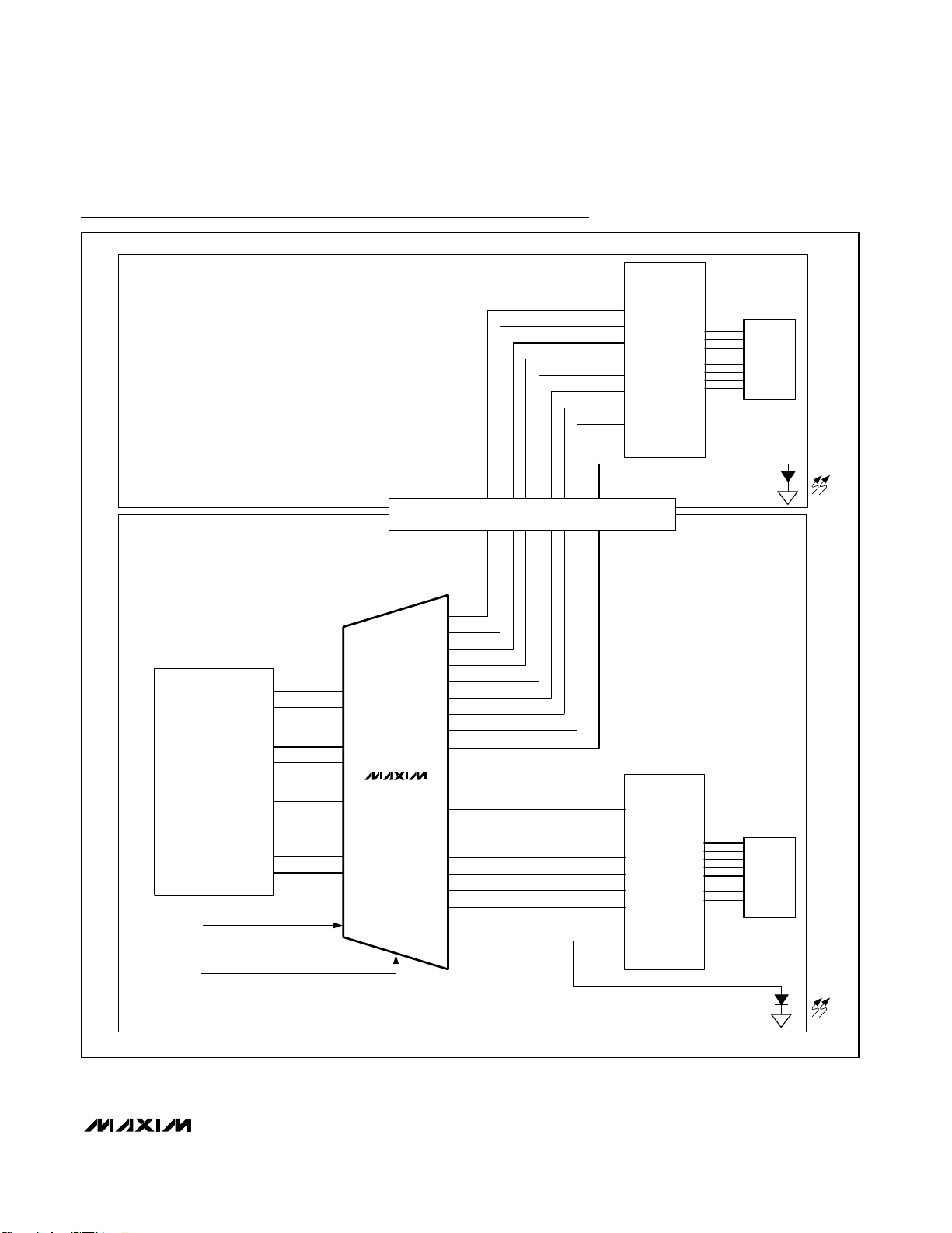
Typical Operating Circuit
The Typical Operating Circuit shows the MAX4890E/
MAX4892E in a 1000 Base-T docking station application.
Power-Supply Sequencing and
Overvoltage Protection
Caution: Do not exceed the absolute maximum ratings.
Stresses beyond the listed ratings may cause permanent damage to the device.
Proper power-supply sequencing is recommended for
all CMOS devices. Always apply V+ before applying
analog signals, especially if the analog signal is not
current limited.
Layout
High-speed switches require proper layout and design
procedures for optimum performance. Keep design-controlled-impedance pc board traces as short as possible.
Ensure that bypass capacitors are as close as possible
to the device. Use large ground planes where possible.
Chip Information
PROCESS: BiCMOS
SEL CONNECTION
0 A_ to _B1, LED_ to _LED1
1 A_ to _B2, LED_ to _LED2
Table 1. Truth Table
Page 8
MAX4890E/MAX4892E
1000 Base-T, ±15kV ESD Protection LAN Switches
8 _______________________________________________________________________________________
V
IH
V
IL
50%
_B1
t
OFF
0V
t
ON
0V
_B2
t
ON
50%
50%
50%
50%
t
OFF
50%
SEL
Figure 2. Turn-On and Turn-Off Times
2.0V
3.0V
1.0V
THE MAX4890E/MAX4892E SWITCHES ARE FULLY BIDIRECTIONAL.
t
PHL
V
H
V
L
2.0V
t
PLH
A_
_B_
PULSE SKEW = t
SK(p)
= |t
PHL
- t
PLH
|
Figure 3. Propagation Delay Times
2.0V
3.0V
1.0V
THE MAX4890E/MAX4892E SWITCHES ARE FULLY BIDIRECTIONAL.
t
PHLX
V
OH
V
OL
2.0V
t
PLHX
A_
_B_
OUTPUT SKEW = t
SK(O)
= |t
PLHY
- t
PLHX
| OR |t
PHLY
- t
PHLX
|
t
PHLY
V
OH
V
OL
2.0V
t
PLHY
_B_
Figure 4. Output Skew
CHARGE-CURRENT
LIMIT RESISTOR
DISCHARGE
RESISTANCE
STORAGE
CAPACITOR
C
s
100pF
R
C
1MΩ
R
D
1500Ω
HIGH-
VOLTAGE
DC
SOURCE
DEVICE
UNDER
TEST
Figure 5. Human Body ESD Test Model (MIL-STD-883, Method 3015)
Page 9
MAX4890E/MAX4892E
1000 Base-T, ±15kV ESD Protection LAN Switches
_______________________________________________________________________________________ 9
NOTEBOOK
DOCKING STATION
ETHERNET
PHY/MAC
TRD0_P
TRD0_N
TRD1_P
TRD1_N
TRD2_P
TRD2_N
TRD3_P
TRD3_N
A0
A1
A2
A3
A4
A5
A6
A7
SEL_DOCK
SEL
_LED2
6B2
7B2
4B2
5B2
2B2
3B2
0B2
1B2
LED_
_LED1
0B1
1B1
2B1
3B1
4B1
5B1
6B1
7B1
LED_OUT
RJ-45
TRANSFORMER
TRANSFORMER
LED
CONNECTOR
RJ-45
LED
MAX4892E
Typical Operating Circuit
Page 10

MAX4890E/MAX4892E
1000 Base-T, ±15kV ESD Protection LAN Switches
10 ______________________________________________________________________________________
Functional Diagrams
0B1
1B1
0B2
1B2
2B1
3B1
2B2
3B2
6B2
7B2
6B1
7B1
4B2
5B2
4B1
5B1
A0
A1
A2
A3
A4
A5
A6
A7
SEL
MAX4890E
0B1
1B1
0B2
1B2
2B1
3B1
2B2
3B2
6B2
7B2
6B1
7B1
4B2
5B2
4B1
5B1
A0
A1
A2
A3
A4
A5
A6
A7
SEL
MAX4892E
LED0
0LED1
0LED2
LED1
LED2
1LED1
1LED2
2LED1
2LED2
Page 11

MAX4890E/MAX4892E
1000 Base-T, ±15kV ESD Protection LAN Switches
______________________________________________________________________________________ 11
Pin Configurations (continued)
32 31 30 29 28 27 26
9 101112131415
18
19
20
21
22
23
24
7
6
5
4
3
2
1
MAX4890E
TQFN
TOP VIEW
A3
A2
N.C.
N.C.
N.C.
N.C.
A4
8
A5
A1
A0
V+
SEL
0B1
1B1
0B2
25
1B2
2B1
3B1
2B2
3B2
4B1
5B1
4B2
17
5B2
7B1
6B2
16
6B1
7B2
N.C.
GND
A7
A6
*EP
*EXPOSED PADDLE CONNECTED TO GND.
+
Page 12

MAX4890E/MAX4892E
1000 Base-T, ±15kV ESD Protection LAN Switches
12 ______________________________________________________________________________________
Package Information
(The package drawing(s) in this data sheet may not reflect the most current specifications. For the latest package outline information,
go to www.maxim-ic.com/packages
.)
QFN THIN.EPS
Page 13
MAX4890E/MAX4892E
1000 Base-T, ±15kV ESD Protection LAN Switches
Maxim cannot assume responsibility for use of any circuitry other than circuitry entirely embodied in a Maxim product. No circuit patent licenses are
implied. Maxim reserves the right to change the circuitry and specifications without notice at any time.
Maxim Integrated Products, 120 San Gabriel Drive, Sunnyvale, CA 94086 408-737-7600 ____________________ 13
© 2006 Maxim Integrated Products is a registered trademark of Maxim Integrated Products, Inc.
Package Information (continued)
(The package drawing(s) in this data sheet may not reflect the most current specifications. For the latest package outline information,
go to www.maxim-ic.com/packages
.)
QFN THIN.EPS
 Loading...