

Page 1
现货库存、技术资料、百科信息、热点资讯,精彩尽在鼎好!
General Description
The MAX4890/MAX4891/MAX4892 high-speed analog
switches meet the needs of 10/100/1000 Base-T applications. These devices switch the signals from two
interface transformers and connect the signals to a single 10/100/1000 Base-T Ethernet PHY, simplifying
docking station design and reducing manufacturing
costs. The MAX4890/MAX4891/MAX4892 can also
route signals from a common interface transformer to
two different boards in board-redundancy applications.
The MAX4890/MAX4891/MAX4892 switches provide an
extremely low capacitance and on-resistance to meet
Ethernet insertion and return-loss specifications. The
MAX4891/MAX4892 feature one and three built-in LED
switches, respectively.
The MAX4890/MAX4891/MAX4892 are available in
space-saving 32- and 36-lead TQFN packages,
significantly reducing the required PC board area.
These devices operate over the -40°C to +85°C temperature range.
Applications
Notebooks and Docking Stations
Servers and Routers with Ethernet Interfaces
Board-Level Redundancy Protection
SONET/SDH Signal Routing
T3/E3 Redundancy Protection
Video Switching
Features
♦ Single +3.0V to +3.6V Power-Supply Voltage
♦ Low On-Resistance (R
ON
): 4Ω (typ), 6.5Ω (max)
♦ Ultra-Low On-Capacitance (CON): 6.5pF (typ)
♦ Low < 200ps Bit-to-Bit Skew
♦ -3dB Bandwidth: 1GHz
♦ Optimized Pin-Out for Easy Transformer and PHY
Interface
♦ Built-In LED Switches for Switching Indicators to
Docking Station
♦ Low 450µA (max) Quiescent Current
♦ Bidirectional 8 to 16 Multiplexer/Demultiplexer
♦ Space-Saving Packages
32-Pin, 5mm x 5mm, TQFN Package
36-Pin, 6mm x 6mm, TQFN Package
MAX4890/MAX4891/MAX4892
10/100/1000 Base-T Ethernet LAN Switch
________________________________________________________________ Maxim Integrated Products 1
Pin Configurations
Ordering Information
19-3577; Rev 1; 8/05
For pricing, delivery, and ordering information, please contact Maxim/Dallas Direct! at
1-888-629-4642, or visit Maxim’s website at www.maxim-ic.com.
All devices are available in the -40°C to +85°C operation temperature range.
Typical Operating Circuit appears at end of data sheet.
Pin Configurations continued at end of data sheet.
PART
MAX4890ETJ 32 TQFN — T-3255-4
MAX4891ETJ 32 TQFN 1 T-3255-4
MAX4892ETX 36 TQFN 3 T-3666-3
PINPACKAGE
LED
SWITCHES
PKG
CODE
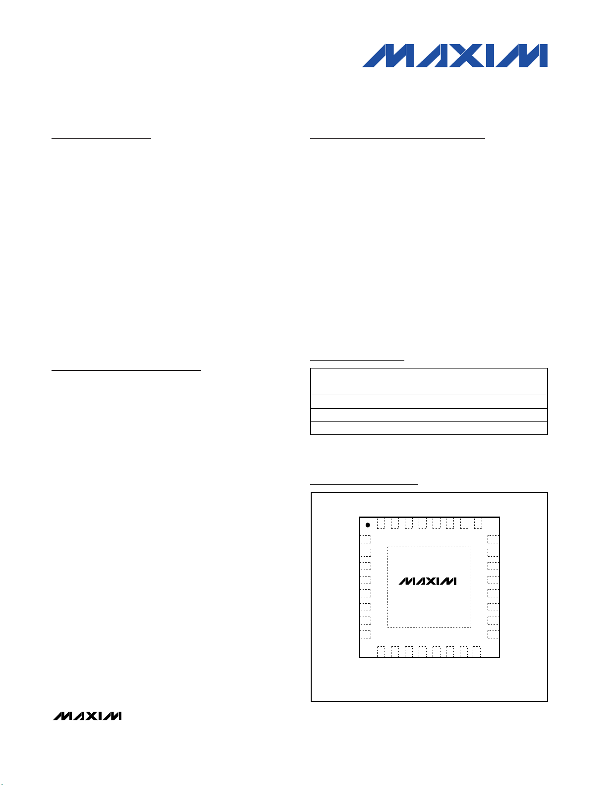
TOP VIEW
A2
1
2
A3
3
N.C.
N.C.
4
5
N.C.
6
N.C.
A4
7
8
A5
A0
V+
A1
32 31 30 29 28 27 26
MAX4890*
9 101112131415
A6
A7
GND
TQFN
SEL
N.C.
1B1
0B1
7B2
6B2
1B2
0B2
25
2B1
24
23
3B1
22
2B2
21
3B2
20
4B1
19
5B1
4B2
18
17
5B2
16
7B1
6B1
Page 2
MAX4890/MAX4891/MAX4892
10/100/1000 Base-T Ethernet LAN Switch
2 _______________________________________________________________________________________
ABSOLUTE MAXIMUM RATINGS
Stresses beyond those listed under “Absolute Maximum Ratings” may cause permanent damage to the device. These are stress ratings only, and functional
operation of the device at these or any other conditions beyond those indicated in the operational sections of the specifications is not implied. Exposure to
absolute maximum rating conditions for extended periods may affect device reliability.
V+ ……………………………………………………… -0.3V to +4V
SEL (Note 1) ………………………………….. -0.3V to (V+ +0.3V)
A_, _B_, LED_, _LED_ .……………………… -0.3V to (V+ +0.3V)
Continuous Current (A_ to _B_) ......................................±120mA
Continuous Current (LED_ to _LED_) .…………………… ±30mA
Peak Current (A_ to _B_)
(pulsed at 1ms, 10% duty cycle) ……………………. ±240mA
Continuous Power Dissipation (T
A
= +70°C)
32-Pin TQFN (derate 34.5mW/°C above +70°C) …….. 2.76W
36-Pin TQFN (derate 26.3mW/°C above +70°C) …….. 2.11W
Operating Temperature Range …………………. -40°C to +85°C
Junction Temperature.……………………………………. +150°C
Storage Temperature Range .…………………. -65°C to +150°C
Lead Temperature (soldering, 10s) .................................+300°C
ELECTRICAL CHARACTERISTICS
(V+ = +3V to +3.6V, TA= T
MIN
to T
MAX
, unless otherwise noted. Typical values are at V+ = 3.3V, TA= +25°C.) (Note 2)
)
)
)
Note 1: Signals on SEL, exceeding V+ or GND, are clamped by internal diodes. Limit forward-diode current to maximum current
rating.
PARAMETER SYMBOL CONDITIONS MIN TYP MAX UNITS
ANALOG SWITCH
On-Resistance R
On-Resistance
LED Switches
R
ONLED
ON
V+ = 3V,
= -40mA,
I
A_
1.5V ≤ V
V+ = 3V, I
A_
_LED_
≤ V+
MAX4891/MAX4892
TA = +25°C 4 5.5
to T
T
MIN
MAX
= -40mA, 1.5V ≤ V
A_
≤ V+,
6.5
Ω
40 Ω
ON
V+ = 3V,
= -40mA,
I
A_
1.5V ≤ V
A_
≤ V+
On-Resistance Match
Between Channels
∆R
(Note 3)
On-Resistance Flatness R
Off-Leakage Current I
On-Leakage Current I
FLAT(ON
LA_(OFF
LA_(ON
V+ = 3V, IA_ = -40mA, V
V+ = 3.6V, VA_ = 0.3V, 3.3V
or V
V
_B1
= 3.3V, 0.3V
_B2
V+ = 3.6V, VA_= 0.3V, 3.3V
or V
V
_B1
= 0.3V, 3.3V or floating
_B2
TA = +25°C 0.5 1.5
to T
T
MIN
MAX
= 1.5V, 2.7V 0.01 Ω
A_
-1 +1
-1 +1
ESD PROTECTION
ESD Protection Human Body Model ±2 kV
SWITCH AC PERFORMANCE
Insertion loss with typical transformer,
Insertion Loss I
LOS
R
= 100Ω, 1MHz < f < 100MHz, Figure 1
L
0.6 dB
(Note 3)
Return loss with
typical transformer,
R
= 100Ω, return
L
loss, f in MHz,
Figure 2 (Note 3)
1MHz < f < 40MHz -19
-13
40MHz < f < 100MHz
+20log
(f/80)
Return Loss
R
R
LOS1
LOS2
Ω
2
µA
dB
Page 3
MAX4890/MAX4891/MAX4892
10/100/1000 Base-T Ethernet LAN Switch
_______________________________________________________________________________________ 3
ELECTRICAL CHARACTERISTICS (continued)
(V+ = +3V to +3.6V, TA= T
MIN
to T
MAX
, unless otherwise noted. Typical values are at V+ = 3.3V, TA= +25°C.) (Note 2)
Note 2: Specifications at -40°C are guaranteed by design.
Note 3: Guaranteed by design.
PARAMETER SYMBOL CONDITIONS MIN TYP MAX UNITS
Differential Crosstalk
SWITCH DYNAMICS
On-Channel -3dB Bandwidth BW RL = 100Ω, Differential pair 1000 MHz
Off-Capacitance C
On-Capacitance C
Off-Capacitance, LED Switches C
On-Capacitance, LED Switches C
Turn-On Time t
Turn-Off Time t
Propagation Delay t
Output Skew Between Ports t
Output Skew Same Port t
SWITCH LOGIC
Input-Voltage Low V
Input-Voltage High V
Input-Logic Hysteresis V
Input Leakage Current I
Operating Supply-Voltage Range V+ 3 3.6 V
Quiescent Supply Current I+ V+ = 3.6V, V
V
CT1
V
CT2
V
CT3
V
DCT1
V
DCT2
V
DCT3
OFF
ON
OFFLED
ONLED
ON
OFF
PLH, tPHLCL
SK(o)
SK(p)
HYST
SEL
Any switch to any
switch R
Figure 3
RL = 100Ω,
Figure 4
f = 1MHz, _B_ inputs 3.5 pF
f = 1MHz, _B_ inputs 6.5 pF
f = 1MHz, _LED inputs 20 pF
f = 1MHz, _LED inputs 22 pF
VA_ = 1V, Figure 5 25 50 ns
V
Skew between A4 and A5 and any other
port, Figure 7
Skew between opposite transitions in same
port
IL
IH
V+ = 3.6V, V
= 100Ω,
L
= 1V, Figure 5 20 40 ns
A_
= 10pF, Figure 6 0.15 ns
SEL
SEL
1MHz < f < 30MHz -45
30MHz < f < 60MHz -40Crosstalk
60MHz < f < 100MHz -35
1MHz < f < 30MHz -60
30MHz < f < 60MHz -55
60MHz < f < 100MHz -50
2.0
= 0 or V+ -5 +5 uA
= 0 or V+ 280 450 µA
0.01 ns
0.07 ns
0.8
100 mV
dB
dB
V
Page 4
MAX4890/MAX4891/MAX4892
10/100/1000 Base-T Ethernet LAN Switch
4 _______________________________________________________________________________________
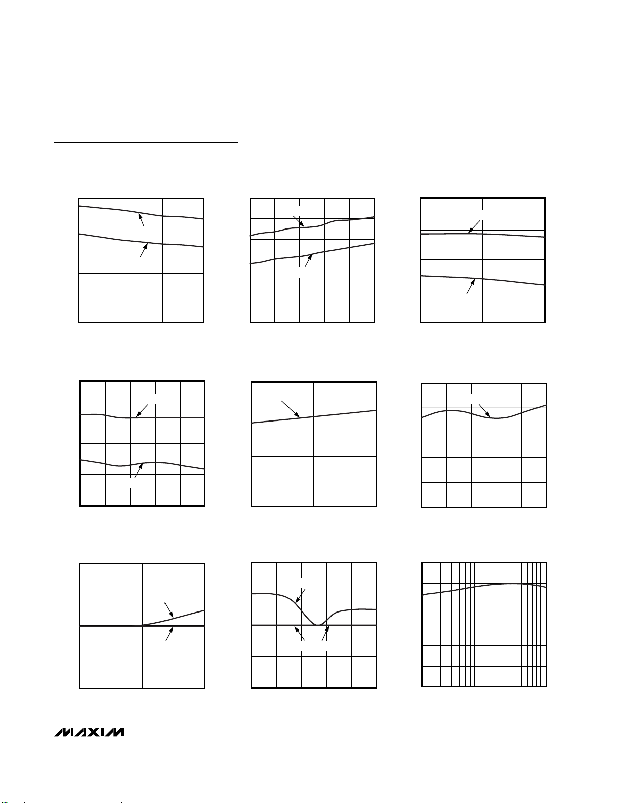
Typical Operating Characteristics
(V+ = 3.3V, TA= +25°C, unless otherwise noted.)
3.0
3.2
3.6
3.4
3.8
4.0
ON-RESISTANCE vs. V
A_
MAX4890 toc01
VA_ (V)
R
ON
(Ω)
01.80.9 2.7 3.6
V+ = 3.0V, 3.3V, 3.6V
0
1
3
2
4
5
ON-RESISTANCE vs. V
A_
MAX4890 toc02
VA_ (V)
R
ON
(Ω)
0 1.1 2.2 3.3
TA = +85°C
TA = -40°C
TA = +25°C
0
6
4
2
8
10
12
14
16
18
20
0 0.9 1.8 2.7 3.6
LED_ ON-RESISTANCE vs. V
A_
MAX4890 toc03
VA_ (V)
R
ONLED
(Ω)
V+ = 3.6V
V+ = 3.3V
V+ = 3.0V
0
6
4
2
8
10
12
14
16
18
20
01.1
2.2
3.3
LED_ ON-RESISTANCE vs. TEMPERATURE
MAX4890 toc04
VA_ (V)
R
ONLED
(Ω)
TA = +25°C
TA = -40°C
TA = +85°C
0
400
200
1000
800
600
1600
1400
1200
1800
-40 10-15 356085
LEAKAGE CURRENT vs. TEMPERATURE
MAX4890 toc05
TEMPERATURE (°C)
LEAKAGE CURRENT (pA)
I
LA_(ON)
I
LA_(OFF)
0
100
5
20
15
25
30
0 1.1 2.2 3.3
CHARGE INJECTION vs. V
A_
MAX4890 toc06
VA_ (V)
CHARGE INJECTION (pC)
150
210
190
170
230
250
270
290
310
330
350
-40 10-15 35 60 85
QUIESCENT SUPPLY CURRENT
vs. TEMPERATURE
MAX4890 toc07
TEMPERATURE (°C)
QUIESCENT SUPPLY CURRENT (µA)
0
400
200
800
600
1000
1200
0 1.1 2.2 3.3
QUIESCENT SUPPLY CURRENT
vs. LOGIC LEVEL
MAX4890 toc08
LOGIC LEVEL (V)
QUIESCENT SUPPLY CURRENT (µA)
0
0.4
0.2
1.0
0.8
0.6
1.6
1.4
1.2
1.8
3.0 3.23.1 3.3 3.4 3.5 3.6
LOGIC THRESHOLD vs. SUPPLY VOLTAGE
MAX4890 toc09
SUPPLY VOLTAGE (V)
LOGIC THRESHOLD (V)
V
TH+
V
TH-
Page 5
MAX4890/MAX4891/MAX4892
10/100/1000 Base-T Ethernet LAN Switch
_______________________________________________________________________________________ 5
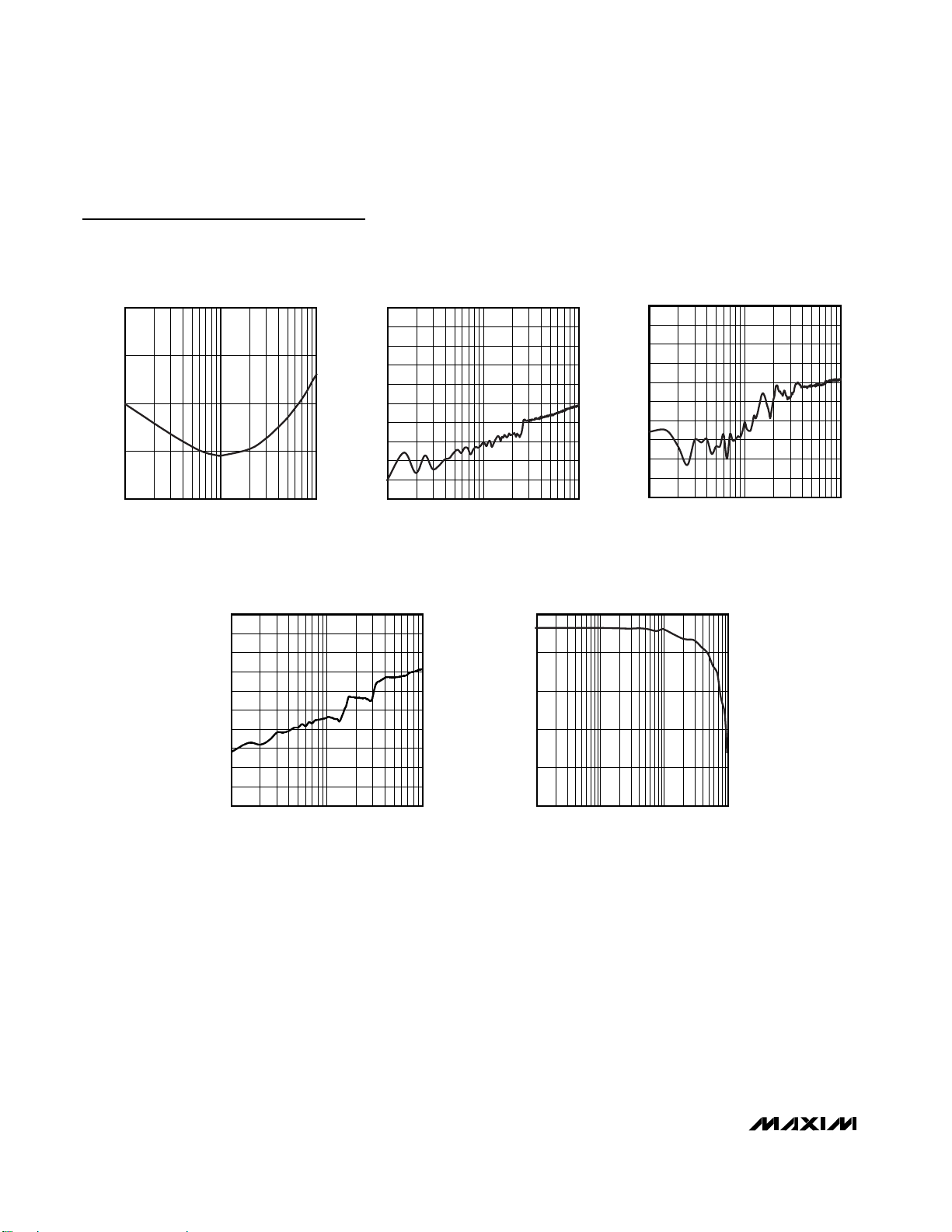
Typical Operating Characteristics (continued)
(V+ = 3.3V, TA= +25°C, unless otherwise noted.)
TURN-ON/-OFF TIME
vs. SUPPLY VOLTAGE
25
20
15
(ns)
OFF
/t
ON
t
10
5
0
3.0 3.2 3.4 3.6
t
ON
t
OFF
SUPPLY VOLTAGE (V)
MAX4890 toc10
(ns)
OFF
/t
ON
t
RISE-/FALL-TIME PROPAGATION DELAY
vs. TEMPERATURE
250
t
200
150
100
OUTPUT RISE-/FALL-TIME DELAY (ps)
t
PHL
PLH
MAX4890 toc13
PULSE SKEW (ps)
TURN-ON/-OFF TIME
vs. TEMPERATURE
30
t
25
20
15
10
5
0
-40 10-15 35 60 85
ON
t
OFF
TEMPERATURE (°C)
PULSE SKEW vs. SUPPLY VOLTAGE
100
t
SK(p)
80
60
40
20
MAX4890 toc11
MAX4890 toc14
RISE-/FALL-TIME PROPAGATION DELAY
vs. SUPPLY VOLTAGE
250
t
PLH
200
150
100
OUTPUT RISE/FALL-TIME DELAY (ps)
50
3.0 3.3 3.6
t
PHL
SUPPLY VOLTAGE (V)
PULSE SKEW vs. TEMPERATURE
100
t
80
60
40
PULSE SKEW (ps)
20
SK(p)
MAX4890 toc12
MAX4890 toc15
50
-40 10-15 35 60 85
TEMPERATURE (°C)
OUTPUT SKEW
vs. SUPPLY VOLTAGE
20
10
0
OUTPUT SKEW (ps)
-10
-20
3.0 3.3 3.6
SUPPLY VOLTAGE (V)
t
SK(o)_FALL
t
SK(o)_RISE
MAX4890 toc16
OUTPUT SKEW (ps)
0
3.0 3.3 3.6
SUPPLY VOLTAGE (V)
OUTPUT SKEW vs. TEMPERATURE
20
t
SK(o)_FALL
10
0
t
SK(o)_RISE
-10
-20
-40 10-15 35 60 85
TEMPERATURE (°C)
0
-40 10-15 35 60 85
DIFFERENTIAL INSERTION LOSS
1
MAX4890 toc17
0
-1
-2
-3
-4
DIFFERENTIAL INSERTION LOSS (dB)
-5
1100
TEMPERATURE (°C)
vs. FREQUENCY
MAX4890 toc18
10
FREQUENCY (MHz)
Page 6
MAX4890/MAX4891/MAX4892
10/100/1000 Base-T Ethernet LAN Switch
6 _______________________________________________________________________________________
Typical Operating Characteristics (continued)
(V+ = 3.3V, TA= +25°C, unless otherwise noted.)
DIFFERENTIAL RETURN LOSS
vs. FREQUENCY
0
-10
-20
-30
DIFFERENTIAL RETURN LOSS (dB)
-40
1 100
10
FREQUENCY (MHz)
0
-10
MAX4890 toc19
-20
-30
-40
-50
-60
-70
DIFFERENTIAL CROSSTALK (dB)
-80
-90
-100
1100
DIFFERENTIAL CROSSTALK
vs. FREQUENCY
MAX4890 toc20
SINGLE-ENDED OFF-ISOLATION (dB)
-100
10
FREQUENCY (MHz)
SINGLE-ENDED OFF-ISOLATION
vs. FREQUENCY
0
-10
-20
-30
-40
-50
-60
-70
-80
-90
1 100
10
FREQUENCY (MHz)
MAX4890 toc21
SINGLE-ENDED CROSSTALK
vs. FREQUENCY
0
-10
-20
-30
-40
-50
-60
-70
-80
SINGLE-ENDED CROSSTALK (dB)
-90
-100
1100
10
FREQUENCY (MHz)
MAX4890 toc22
0
-1
-2
-3
-4
SINGLE-ENDED INSERTION LOSS (dB)
-5
SINGLE-ENDED INSERTION LOSS
vs. FREQUENCY
1 1000
FREQUENCY (MHz)
10010
MAX4890 toc23
Page 7

MAX4890/MAX4891/MAX4892
10/100/1000 Base-T Ethernet LAN Switch
_______________________________________________________________________________________ 7
Pin Description
PIN
MAX4890 MAX4891 MAX4892
31, 32, 1, 2,
7–10
— 3 4 LED0 LED0 Input
— 4 5 0LED1 0LED1 Output. Connects LED0 to 0LED1 when SEL = 0.
— 5 6 0LED2 0LED2 Output. Connects LED0 to 0LED2 when SEL = 1.
3–6, 12 6, 12 — N.C. No Connection. Not internally connected.
11 11 11 GND Ground
— — 12 LED1 LED1 Input
— — 13 1LED1 1LED1 Output. Connects LED1 to 1LED1 when SEL = 0.
— — 14 1LED2 1LED2 Output. Connects LED1 to 1LED2 when SEL = 1.
13, 14, 17,
18, 21, 22,
25, 26
15, 16, 19,
20, 23, 24,
27, 28
29 29 27 SEL Select Input. Selects switch connection. See the Truth Table (Table 1).
— — 32 2LED2 2LED2 Output. Connects LED2 to 2LED2 when SEL = 1.
— — 33 2LED1 2LED1 Output. Connects LED2 to 2LED1 when SEL = 0.
— — 34 LED2 LED2 Input
30 30 35 V+ Positive Supply-Voltage Input
EP EP EP EP
31, 32, 1, 2,
7–10
13, 14, 17,
18, 21, 22,
25, 26
15, 16, 19,
20, 23, 24,
27, 28
36, 1, 2, 3,
7–10
15, 16, 19,
20, 23, 24,
28, 29
17, 18, 21,
22, 25, 26,
30, 31
NAME FUNCTION
A0–A7 Differential PHY Interface Pair. Connects to the Ethernet PHY.
7B2–0B2 B2 Differential Transformer Pair
7B1–0B1 B1 Differential Transformer Pair
Exposed Paddle. Not internally connected. Leave unconnected or connect to
ground.
Page 8

MAX4890/MAX4891/MAX4892
10/100/1000 Base-T Ethernet LAN Switch
8 _______________________________________________________________________________________
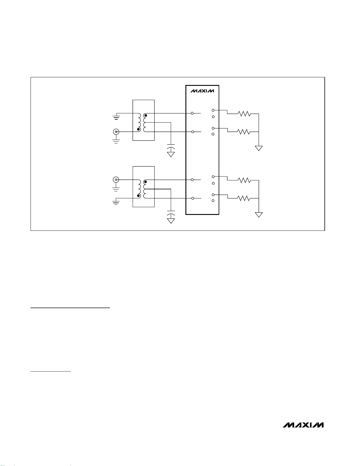
Test Circuits
Figure 1. Differential Insertion Loss
Figure 2. Differential Return Loss
A0
36
A1
1
MAX4892
36 TQFN
0B1
3B1
50Ω
TRACE
31
50Ω
TRACE
30
5
4
6
C2
0.01µF
PULSE H5007
24-PIN PACKAGE
INSERTION LOSS
NETWORK
ANALYZER
50Ω
TRACE
1
3
MINI CKT
BALUN
50:100
CB1
50Ω
TRACE
50Ω
TRACE
6
5
4
RETURN LOSS
MAX4892
36 TQFN
A2
2
R16
49.9Ω
A3
3
R17
49.9Ω
3B1
25
50Ω
TRACE
50Ω
TRACE
5
4
6
C2
0.01µF
PULSE H5007
24-PIN PACKAGE
BALUN
100:50
CB3
MINI CKT
BALUN
4
5
6
100:50
3
1
TRACE
50Ω
3
1
TRACE
50Ω
NETWORK
ANALYZER
NETWORK
ANALYZER
50Ω
TRACE
20
21
50Ω
TRACE
19
R1
75Ω
C3
1000pF
50Ω
TRACE
20
21
19
50Ω
TRACE
R1
75Ω
MINI CKT
4
5
6
CB3
C3
1000pF
Page 9

Detailed Description
The MAX4890/MAX4891/MAX4892 are high-speed analog switches targeted for 10/100/1000 Base-T applications. In a typical application, the MAX4890/MAX4891/
MAX4892 switch the signals from two separate interface transformers and connect the signals to a single
10/100/1000 Base-T Ethernet PHY (see the Typical
Operating Circuit). This configuration simplifies docking
station design by avoiding signal reflections associated
with unterminated transmission lines in a T configuration. The MAX4891 and MAX4892 also include LED
switches that allow the LED output signals to be routed
to a docking station along with the Ethernet signals.
See the Functional Diagrams.
The MAX4890/MAX4891/MAX4892 switches provide
an extremely low capacitance and on-resistance
to meet Ethernet insertion and return-loss specifications. The MAX4891/MAX4892 feature one and three
built-in LED switches, respectively.
The MAX4890/MAX4891/MAX4892 incorporate a unique
architecture design utilizing only n-channel switches
within the main Ethernet switch, reducing I/O capacitance and channel resistance. An internal two-stage
charge pump with a nominal output of 7.5V provides the
high voltage needed to drive the gates of the n-channel
switches, while maintaining a consistently low R
ON
throughout the input signal range. An internal bandgap
reference set to 1.23V and an internal oscillator running
at 2.5MHz provide proper charge-pump operation.
Unlike other charge-pump circuits, the MAX4890/
MAX4891/MAX4892 include internal flyback capacitors,
reducing design time, board space, and cost.
Digital Control Inputs
The MAX4890/MAX4891/MAX4892 provide a single
digital control SEL. SEL controls the switches as well as
the LED switches as shown in Table 1.
MAX4890/MAX4891/MAX4892
10/100/1000 Base-T Ethernet LAN Switch
_______________________________________________________________________________________ 9
Table 1. Truth Table
Figure 3. Single-Ended Bandwidth, Crosstalk and Off-Isolation
Test Circuits (continued)
SINGLE-ENDED BANDWIDTH
NETWORK
ANALYZER
SINGLE-ENDED CROSSTALK
NETWORK
ANALYZER
NETWORK
ANALYZER
SINGLE-ENDED OFF-ISOLATION
NETWORK
ANALYZER
50Ω TRACE
50Ω TRACE
50Ω TRACE
50Ω TRACE
R15
49.9Ω
MAX4892
36 TQFN
A0
36
A2
2
A3
3
A4
7
0B1
31
2B1
26
4B1
22
3B1
25
50Ω TRACE
R13
49.9Ω
R14
49.9Ω
NETWORK
ANALYZER
50Ω TRACE
NETWORK
ANALYZER
SEL CONNECTION
0 A_ to _B1, LED_ to _LED1
1 A_ to _B2, LED_ to _LED2
Page 10
MAX4890/MAX4891/MAX4892
Analog Signal Levels
The on-resistance of the MAX4890/MAX4891/MAX4892
is very low and stable as the analog input signals are
swept from ground to V+ (see the Typical Operating
Characteristics). The switches are bidirectional, allowing A_ and _B_ to be configured as either inputs or outputs.
ESD Protection
The MAX4890/MAX4891/MAX4892 are characterized
using the Human Body Model for ±2kV of ESD protection. Figure 8 shows the Human Body Model, and Figure
9 shows the current waveform the Human Body Model
generates when discharged into a low-impedance load.
This model consists of a 100pF capacitor charged to the
ESD voltage of interest, which is then discharged into the
test device through a 1.5kΩ resistor.
Applications Information
Typical Operating Circuit
The Typical Operating Circuit depicts the MAX4890/
MAX4891/MAX4892 in a 10/100/1000 Base-T docking
station application.
Line-Card Redundancy (Ethernet T3/E3)
Figure 10 shows the MAX4890/MAX4891/MAX4892 in a
line-card redundancy configuration.
Power-Supply Sequencing and
Overvoltage Protection
Caution: Do not exceed the absolute maximum ratings.
Stresses beyond the listed ratings may cause permanent damage to the device.
Proper power-supply sequencing is recommended for
all CMOS devices. Always apply V+ before applying
analog signals, especially if the analog signal is not
current limited.
Layout
High-speed switches require proper layout and design
procedures for optimum performance. Keep designcontrolled-impedance printed circuit board traces as
short as possible. Ensure that bypass capacitors are as
close to the device as possible. Use large ground
planes where possible.
10/100/1000 Base-T Ethernet LAN Switch
10 ______________________________________________________________________________________
Figure 4. Differential Crosstalk
DIFFERENTIAL CROSSTALK TRANSMIT CKT
MAX4892
MINI CKT
BALUN
1
NETWORK
ANALYZER
DIFFERENTIAL CROSSTALK RECEIVE CKT
NETWORK
ANALYZER
50Ω
TRACE
50Ω
TRACE
3
50:100
MINI CKT
BALUN
1
3
50:100
6
4
CB4
50Ω
6
TRACE
5
4
CB5
50Ω
TRACE
36-TQFN
AB1
5B1
6B1
7B1
22
R3
21
18
17
49.9Ω
R4
49.9Ω
R3
49.9Ω
R4
49.9Ω
A4
7
A5
8
A6
9
A7
10
Page 11

MAX4890/MAX4891/MAX4892
10/100/1000 Base-T Ethernet LAN Switch
______________________________________________________________________________________ 11
SEL
Figure 5. ENABLE and DISABLE Times
Figure 6. Propagation Delay Times
Figure 7. Output Skew
Figure 8. Human Body ESD Test Model
2.5V
3.0V
1.25V
t
ON
90%
t
OFF
10%
A_
t
PLHX
1.25V
t
PHLX
2.0V
0V
A_
t
OFF
90%
0V
t
ON
A_
90%
A_
t
PLH
_B_
PULSE SKEW = t
SK(p)
= |t
PHL
1.0V
t
PHL
V
OH
2.0V
V
OL
- t
|
PLH
THE MAX4890/MAX4891/MAX4892 SWITCHES ARE FULLY BIDIRECTIONAL.
0V
3.0V
2.0V
1.0V
R
C
1MΩ
CHARGE-CURRENT
V
OH
LIMIT RESISTOR
R
D
1500Ω
DISCHARGE
RESISTANCE
_B_
t
PLHY
_B_
PULSE SKEW = t
THE MAX4890/MAX4891/MAX4892 SWITCHES ARE FULLY BIDIRECTIONAL.
SK(p)
= |t
PHLY
- t
| OR |t
- t
PHLy
PHLx
|
PLHX
t
PHLY
2.0V
V
HIGH-
VOLTAGE
OL
V
OH
2.0V
V
OL
DC
SOURCE
C
100pF
STORAGE
s
CAPACITOR
DEVICE
UNDER
TEST
Page 12
MAX4890/MAX4891/MAX4892
10/100/1000 Base-T Ethernet LAN Switch
12 ______________________________________________________________________________________
Figure 9. Human Body Model Current Waveform
Figure 10. Typical Application for Line-Card Redundancy
ETHERNET
PHYs
OR
T3/E3 LIUs
PRIMARY CARD
ETHERNET
PHYs
OR
T3/E3 LIUs
PROTECTION CARD
MAX4890
MAX4891
MAX4892
PROTECTION
SWITCH
TRANSFORMER
AMPERES
IP 100%
90%
36.8%
10%
PEAK-TO-PEAK RINGING
I
r
(NOT DRAWN TO SCALE)
0
0
t
RL
TIME
t
DL
CURRENT WAVEFORM
SWITCHING CARD
Page 13

MAX4890/MAX4891/MAX4892
10/100/1000 Base-T Ethernet LAN Switch
______________________________________________________________________________________ 13
Typical Operating Circuit
DOCKING STATION
NOTEBOOK
ETHERNET
PHY/MAC
LED_OUT
TRD0_P
TRD0_N
TRD1_P
TRD1_N
TRD2_P
TRD2_N
TRD3_P
TRD3_N
A0
MAX4890/MAX4891/MAX4892
A1
A2
A3
A4
A5
A6
A7
LED_
SEL
_LED2
_LED1
0B2
1B2
2B2
3B2
4B2
5B2
6B2
7B2
0B1
1B1
2B1
3B1
4B1
5B1
6B1
7B1
CONNECTOR
TRANSFORMER
RJ-45
LED
TRANSFORMER
RJ-45
SEL_DOCK
LED
Page 14

MAX4890/MAX4891/MAX4892
10/100/1000 Base-T Ethernet LAN Switch
14 ______________________________________________________________________________________
Functional Diagrams
A0
A1
A2
A3
A4
A5
A6
A7
LED0
SEL
SEL
A0
A1
A2
A3
A4
A5
A6
A7
MAX4890
0B1
1B1
0B2
1B2
2B1
3B2
2B1
3B2
4B1
5B1
4B2
5B2
6B1
7B1
6B2
7B2
0B1
1B1
0B2
1B2
2B1
3B2
2B1
3B2
4B1
5B1
4B2
5B2
6B1
7B1
6B2
7B2
0LED1
0LED2
MAX4891
Page 15

MAX4890/MAX4891/MAX4892
10/100/1000 Base-T Ethernet LAN Switch
______________________________________________________________________________________ 15
Functional Diagrams (continued)
LED0
LED1
LED2
SEL
A0
A1
A2
A3
A4
A5
A6
A7
0B1
1B1
0B2
1B2
2B1
3B2
2B1
3B2
4B1
5B1
4B2
5B2
6B1
7B1
6B2
7B2
0LED1
0LED2
1LED1
1LED2
2LED1
2LED2
MAX4892
Page 16
MAX4890/MAX4891/MAX4892
10/100/1000 Base-T Ethernet LAN Switch
16 ______________________________________________________________________________________
Chip Information
TRANSISTOR COUNT: 948
PROCESS: BiCMOS
32 31 30 29 28 27 26
9 101112131415
18
19
20
21
22
23
24
7
6
5
4
3
2
1
MAX4891
TQFN
TOP VIEW
A3
A2
LED0
0LED1
0LED2
N.C.
A4
8
A5
A1
A0
V+
SEL
0B1
1B1
0B2
25
1B2
2B1
3B1
2B2
3B2
4B1
5B1
4B2
17
5B2
7B1
6B2
16
6B1
7B2
N.C.
GND
A7
A6
TQFN
SEL
2B1
2B2
3B2
4B2
5B2
4B1
5B1
3B1
A3
LED0
0LED1
A4
A5
A6
A1
1
2
3
4
5
6
7
8
9
27
26
25
24
23
22
21
20
19
1LED2
7B2
6B2
6B1
1LED1
LED1
GND
A7
MAX4892
0LED2
7B1
A2
A0
10
11
12
13
14
15
16
17
18
36
35
34
33
32
31
30
29
28
0B2
V+
LED2
2LED1
2LED2
0B1
1B1
1B2
Pin Configurations (continued)
Page 17

MAX4890/MAX4891/MAX4892
10/100/1000 Base-T Ethernet LAN Switch
______________________________________________________________________________________ 17
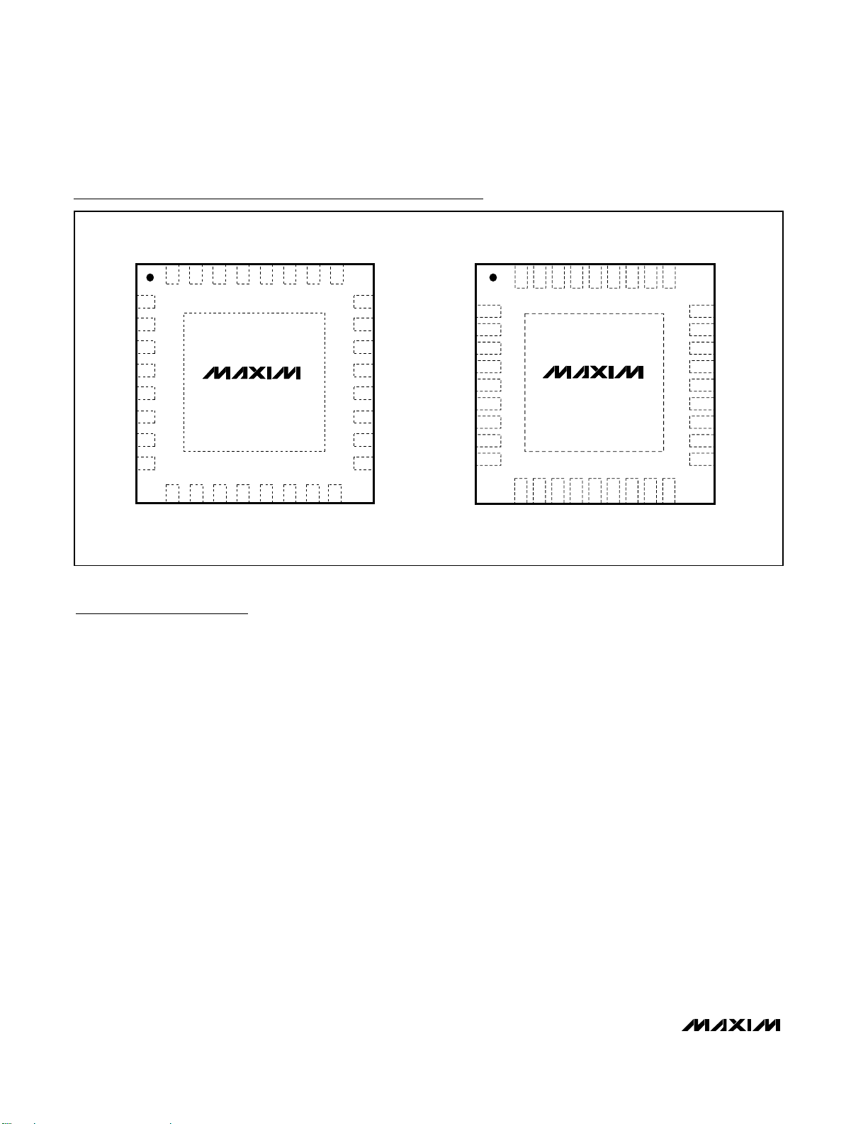
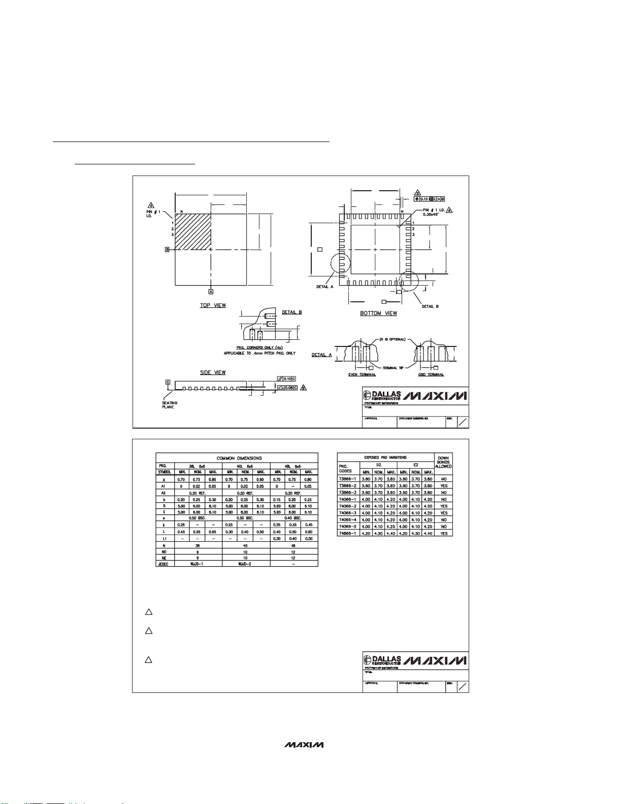
Package Information
(The package drawing(s) in this data sheet may not reflect the most current specifications. For the latest package outline information,
go to www.maxim-ic.com/packages
.)
C
D
XXXXX
D2
C
D/2
E/2
E
e
L1
0.10 C
A
0.08 C
A3
A1
(NE-1) X e
DETAIL A
L
L
k
e
(ND-1) X e
L
e e
PACKAGE OUTLINE,
16, 20, 28, 32, 40L THIN QFN, 5x5x0.8mm
D2/2
b
0.10 M C A B
H
LL
1
2
QFN THIN.EPS
L
E2/2
C
E2
L
DETAIL B
PIN # 1 I.D.
0.35x45°
CC
L
e/2
21-0140
MARKING
PIN # 1
I.D.
-DRAWING NOT TO SCALE-
PKG.
SYMBOL
A
A1
A3
b
D
E
e
k
L
L1
N
ND
NE
JEDEC
NOTES:
1. DIMENSIONING & TOLERANCING CONFORM TO ASME Y14.5M-1994.
2. ALL DIMENSIONS ARE IN MILLIMETERS. ANGLES ARE IN DEGREES.
3. N IS THE TOTAL NUMBER OF TERMINALS.
4. THE TERMINAL #1 IDENTIFIER AND TERMINAL NUMBERING CONVENTION SHALL
CONFORM TO JESD 95-1 SPP-012. DETAILS OF TERMINAL #1 IDENTIFIER ARE
OPTIONAL, BUT MUST BE LOCATED WITHIN THE ZONE INDICATED. THE TERMINAL #1
IDENTIFIER MAY BE EITHER A MOLD OR MARKED FEATURE.
5. DIMENSION b APPLIES TO METALLIZED TERMINAL AND IS MEASURED BETWEEN
0.25 mm AND 0.30 mm FROM TERMINAL TIP.
6. ND AND NE REFER TO THE NUMBER OF TERMINALS ON EACH D AND E SIDE RESPECTIVELY.
7. DEPOPULATION IS POSSIBLE IN A SYMMETRICAL FASHION.
8. COPLANARITY APPLIES TO THE EXPOSED HEAT SINK SLUG AS WELL AS THE TERMINALS.
9. DRAWING CONFORMS TO JEDEC MO220, EXCEPT EXPOSED PAD DIMENSION FOR T2855-1,
T2855-3, AND T2855-6.
10. WARPAGE SHALL NOT EXCEED 0.10 mm.
11. MARKING IS FOR PACKAGE ORIENTATION REFERENCE ONLY.
12. NUMBER OF LEADS SHOWN ARE FOR REFERENCE ONLY.
13. LEAD CENTERLINES TO BE AT TRUE POSITION AS DEFINED BY BASIC DIMENSION "e", ±0.05.
-DRAWING NOT TO SCALE-
COMMON DIMENSIONS
16L 5x5
MIN. MAX.NOM.
0.70 0.800.75
0.05
0.02
0.20 REF.
0.350.30
0.25
5.10
5.00
4.90
5.105.00
4.90
0.80 BSC.
0.250--
0.30 0.500.40
---
16
4
4
WHHB
MIN.
0.70
0.25
4.90
4.90
0.25
0.45
0
---
20L 5x5
NOM.
0.75
0.02
0.20 REF.
0.30
5.00
5.00
0.65 BSC.
0.55
20
5
5
WHHC
MAX.
0.80
0.05
0.35
5.10
5.10
0.65
28L 5x5
NOM.
MIN.
0.70
0.75
0
0.02
0.20 REF.
0.20
5.00
4.90
4.90
0.50 BSC.
--
0.25
0.45
---
WHHD-1
32L 5x5
MAX.
MIN.
0.80
0.70
0.05
0
0.20 REF.
0.30
0.20 0.25 0.30
0.25
5.10
4.90
5.10
5.00
4.90
0.50 BSC.
--
0.25
0.65
0.55
0.30
---
28
7
7
WHHD-2
NOM.
0.75
0.02
0.40
5.00
5.00
32
8
8
MAX.
MIN.
0.80
0.70
0.05
0.15
5.10
4.90
5.10
4.90 5.00
--
0.25 0.35 0.45
0.50
0.30
40L 5x5
NOM.
0.75 0.80
0.20 REF.
5.00 5.10
0.40 BSC.
0.40 0.50
40
10
10
-----
MAX.
0.0500.02
0.250.20
5.10
0.600.40 0.50
EXPOSED PAD VARIATIONS
PKG.
CODES
T1655-1 3.203.00 3.10 3.00 3.10 3.20
T2855-2 2.60 2.602.80 2.70 2.80
T2855-3 3.15 3.25 3.35 3.15 3.25 3.35
T2855-4 2.60 2.70 2.80 2.60 2.70 2.80
T2855-5 2.60 2.70 2.80 2.60 2.70 2.80
T2855-6 3.15 3.25 3.35 3.15 3.25 3.35
T2855-7 2.60 2.70
T3255-2
D2
MAX.
NOM.MIN.
MIN.E2NOM. MAX.
3.203.00T1655-2 3.10 3.00 3.10 3.20 YES
3.20
3.00T2055-2 3.10
3.353.15T2055-5 3.25 3.15 3.25 3.35
3.353.15T2855-1 3.25 3.353.15 3.25
2.70
2.80
3.35
3.15T2855-8 3.25 3.15 3.25 3.35
3.35
3.15T2855N-1 3.25 3.15 3.25 3.35
3.20
3.00
3.10
3.203.00 3.10T3255-3 3.203.00 3.10
3.203.00 3.10T3255-4 3.203.00 3.10
3.203.10T3255N-1 3.00
3.30T4055-1 3.20 3.40 3.20 3.30 3.40
PACKAGE OUTLINE,
16, 20, 28, 32, 40L THIN QFN, 5x5x0.8mm
3.203.00 3.10
3.103.00 3.203.103.00 3.20T2055-4
2.60 2.70 2.80
3.00 3.10 3.20
3.203.103.00
SEE COMMON DIMENSIONS TABLE
**
21-0140
±0.15
0.40
0.40
DOWN
L
BONDS
ALLOWED
NO
**
**
NO3.203.103.003.10T1655N-1 3.00 3.20
**
**
NO
YES3.103.00 3.203.103.00 3.20T2055-3
**
NO
**
YES
NO
**
NO
**
YES
**
YES
**
NO
**
NO
**
YES
**
YES
NO
**
NO
**
YES
**
NO
**
NO
**
YES
**
2
H
2
Page 18
MAX4890/MAX4891/MAX4892
10/100/1000 Base-T Ethernet LAN Switch
Maxim cannot assume responsibility for use of any circuitry other than circuitry entirely embodied in a Maxim product. No circuit patent licenses are
implied. Maxim reserves the right to change the circuitry and specifications without notice at any time.
18 ____________________Maxim Integrated Products, 120 San Gabriel Drive, Sunnyvale, CA 94086 408-737-7600
© 2005 Maxim Integrated Products Printed USA is a registered trademark of Maxim Integrated Products, Inc.
Package Information (continued)
(The package drawing(s) in this data sheet may not reflect the most current specifications. For the latest package outline information,
go to www.maxim-ic.com/packages
.)
D
D/2
D2
C
L
k
b
D2/2
E/2
(NE-1) X e
L
L1
e
A1 A2
E
A
(ND-1) X e
C
L
e
e e
PACKAGE OUTLINE
36, 40, 48L THIN QFN, 6x6x0.8mm
21-0141
E2/2
C
E2
L
k
L
C
L
QFN THIN 6x6x0.8.EPS
LL
1
E
2
NOTES:
1. DIMENSIONING & TOLERANCING CONFORM TO ASME Y14.5M-1994.
2. ALL DIMENSIONS ARE IN MILLIMETERS. ANGLES ARE IN DEGREES.
3. N IS THE TOTAL NUMBER OF TERMINALS.
4. THE TERMINAL #1 IDENTIFIER AND TERMINAL NUMBERING CONVENTION SHALL CONFORM TO JESD 95-1
SPP-012. DETAILS OF TERMINAL #1 IDENTIFIER ARE OPTIONAL, BUT MUST BE LOCATED WITHIN THE
ZONE INDICATED. THE TERMINAL #1 IDENTIFIER MAY BE EITHER A MOLD OR MARKED FEATURE.
5. DIMENSION b APPLIES TO METALLIZED TERMINAL AND IS MEASURED BETWEEN 0.25 mm AND 0.30 mm
FROM TERMINAL TIP.
6. ND AND NE REFER TO THE NUMBER OF TERMINALS ON EACH D AND E SIDE RESPECTIVELY.
7. DEPOPULATION IS POSSIBLE IN A SYMMETRICAL FASHION.
8. COPLANARITY APPLIES TO THE EXPOSED HEAT SINK SLUG AS WELL AS THE TERMINALS.
9. DRAWING CONFORMS TO JEDEC MO220, EXCEPT FOR 0.4mm LEAD PITCH PACKAGE T4866-1.
10. WARPAGE SHALL NOT EXCEED 0.10 mm.
PACKAGE OUTLINE
36, 40, 48L THIN QFN, 6x6x0.8mm
21-0141
2
E
2
 Loading...